 S. Ağca
 G. Çankaya1
95% of researchers rate our articles as excellent or good
Learn more about the work of our research integrity team to safeguard the quality of each article we publish.
Find out more
ORIGINAL RESEARCH article
Front. Energy Res. , 28 July 2023
Sec. Solar Energy
Volume 11 - 2023 | https://doi.org/10.3389/fenrg.2023.1215712
The development of wide-bandgap Cu(In,Ga)Se2 thin films is crucial in order to reach the theoretical Shockley–Queisser limit values in single-crystal solar cells. However, the performance of solar cells based on wide-bandgap thin film absorbers has lagged significantly compared to that of their narrow-bandgap counterparts. Herein, we develop a feasible strategy to improve the photovoltaic performance of wide-bandgap Cu(In,Ga)Se2 chalcopyrite thin-film solar cells by simultaneously doping with both RbF PDT and Te2− anions as dopants in the absorber layer during the three-stage co-evaporation process. Besides inducing significant change in the GGI gradient, the synergistic effect of the Te2− anion dopant is rather beneficial in terms of controlling grain size, defects in grain boundaries, and charge carrier lifetime for encouraging charge separation and extraction, which contributes to simultaneously boosting short-circuit current density and fill factor. Te-poor devices afford an impressive efficiency of 9.58%, compared to 6.43% for control devices. More importantly, the efficiency and Voc values obtained for wide-bandgap-based thin-film solar cells containing Te anions were the highest compared to their counterparts as reported in the literature. These results demonstrate the role of Te2− anions in wide-bandgap absorber thin films on the photovoltaic performance of thin-film solar cells and the potential of this approach for use in reasonable and effective design of highly efficient wide-bandgap thin-film solar cells.
Given the emergence of climate change as one of the most crucial environmental challenges in today’s world, solar energy has become one of the most important candidate alternatives to fossil fuels in combating climate change (Scheer et al., 2004; Sönmezoğlu Ates et al., 2016; Kamikawa et al., 2022; Kaya et al., 2022; Liu et al., 2022;Mabvuer et al., 2022; Oliveira et al., 2022). Among the various types of solar cells, one of the most important technologies in the field of solar energy, Cu(In,Ga)Se2 thin-film solar cells (TFSCs) have emerged as currently one of the most promising photovoltaic technologies, owing to their very high power conversion efficiency (PCE) of 23.4%, high absorption coefficient, effective usage of raw materials, and tunable direct bandgap (Wei et al., 1998; Guillemoles, 2002; Lundberg et al., 2005; Theelen and Daume, 2016; Naghavi et al., 2017). In spite of their high efficiency, Cu(In,Ga)Se2 TFSCs still remain less efficient compared to both their theoretically achievable efficiency (33.7%) based on the Shockley–Queisser (S-Q) limit for single-junction solar cells (Shockley and Queisser, 1961) and other types of solar cells, such as single-crystal silicon (26.80%) and perovskite solar cells (26.08%). This is attributable to the preference for narrow-bandgap materials (1.0–1.1 eV) instead of materials with the ideal bandgap value (1.4 eV) as defined by the S-Q limit, causing major loss in open-circuit voltage (Voc) and reducing short-circuit current (Jsc) and fill factor (FF) (Polman et al., 2016; NREL Best Research-Cell Efficiency Chart, 2022). In order to reach theoretical efficiency, it is of major importance to choose suitable wide-bandgap absorber materials, with a bandgap between 1.3 and 1.4 eV.
To adjust the bandgap of Cu(In,Ga)Se2 TFSCs, the most effective approaches are as follows. First, by changing the (Ga)/(In+Ga) (GGI) ratio, the bandgap can be varied from 1.02 eV (for CuInSe2) to 1.68 eV (for CuGaSe2) (Gloeckler and Sites, 2005; Witte et al., 2015; Zahedi-Azad et al., 2020). However, research to date has shown that the TFSCs with the highest efficiency are based on bandgaps in the 1.2–1.3 eV range achieved in films where the GGI ratio is between 0.25 and 0.30. As the bandgap is increased further, Jsc falls off precipitously while Voc remains nearly constant. This limits the use of Cu(In,Ga)Se2 films with high Ga concentration as a wide-bandgap absorber layer in TFSCs. Second, by altering the anion elements (the Se/S ratio), the bandgap of these materials can be controlled in the range of 1.04 eV (CuInSe2) to 1.53 eV (CuInS2). Nevertheless, when Ga is incorporated into these matrices, the bandgap increases considerably to values between 1.68 eV (CuGaSe2) and 2.43 eV (CuGaS2) (Ishizuka et al., 2018). At the same time, precise control of the S/Se ratio is very difficult because of the thermal annealing process during fabrication, which poses major challenges at this stage, such as the formation of non-stoichiometric compositions (Kim et al., 2012; Kobayashi et al., 2015; Ju et al., 2017). Based on the aforementioned results, we see that gradients of the Ga/In cation and Se/S anion are a major limitation on improvements to the performance of wide-bandgap absorber-based cells; research into alternative approaches to effective control of bandgaps therefore needs immediate attention.
Another promising approach for control of the bandgap is to use tellurium (Te) as an anion dopant, leading to a wider distribution of anisotropic electrons and thus an enlarged electropositive region via increase in the strength of the chalcogen bond, as a result of the lower electronegativity and higher radius compared to those of Se and S (Rosenfield et al., 1977; Sönmezoğlu, 2014; Akın et al., 2017; Steinke et al., 2023). Another outstanding property is that Te has a lower effective mass (0.45 mo) than selenium (1.40mo), which implies an increase in mobility of the hole carriers of absorber materials (Caldwell and Fan, 1959; Beyer et al., 1971; Madelung, 2012; Sönmezoğlu et al., 2013; Sönmezoğlu and Akman, 2014). A detailed literature search revealed that there have been many attempts to examine the effects of a Te2− anion on the microstructural, morphological, optical, and electrical properties of chalcopyrite thin films (Mise and Nakada, 2010a; Fiat et al., 2013a; Fiat et al., 2013b; Fiat et al., 2014a; Fiat et al., 2014b; Karatay et al., 2017; Atasoy et al., 2018); surprisingly, however, few studies have focused on the impact of Te2− anions on the photovoltaic parameters of wide-bandgap chalcopyrite absorber-based TFSCs. The first results on the utilization of a Te2− anion in wide-bandgap absorber materials for solar cells were reported by Kim et al. (2013). They reported on the synthesis of colloidal CuInTe2–xSex gradient-alloyed quantum dots (QDs) via a simple hot injection method and their use as a p-type wide-bandgap absorber layer (1.40 eV) in heterojunction solar cells. However, their device architecture was designed as a heterojunction structure with a CuInTe2–xSex p-type absorber layer and n-type TiO2 materials instead of TFSCs, and therefore, the solution-processed heterojunction solar cell based on the gradient-alloyed Cu0.23In0.36Te0.19Se0.22 QDs remained at a low efficiency of 3.8%. In a second study, Hamid et al. (2019) investigated the use of single-step evaporation-processed CuInTe2 doped with manganese element as a wide-bandgap absorber layer (1.45 eV) in TFSCs, achieving a PCE of 1.8%. In addition to the poor performance exhibited by their TFSCs, the existence of surface disorder and amorphous structure originating from the fabrication process created negative effects. Thus, in order to design wide-bandgap absorber materials that are suitable for highly efficient TFSC applications, it is necessary to understand the role of Te2− anions in chalcopyrite thin film with respect to device performance.
In this study, a series of RbF post-deposition-treated Cu(In,Ga)Se2 wide-bandgap absorbers with Te2− anions incorporated as a dopant were grown via three-stage co-evaporation, and the effects of the Te2− anion on the photovoltaic performance of these wide-bandgap absorber layer-based TFSCs were explored for the first time. The incorporation of the Te2− anion into the Cu(In,Ga)Se2 thin films encouraged more uniform morphology and well-controlled growth of large grains with high crystallinity. In addition, it was observed that the use of Te2− anions as an additive reduced hole-trap density in the bulk materials and led to enhanced carrier lifetime, thus giving rise to pronounced enhancement of Jsc and FF. As a result, Te-poor Cu(In,Ga)(Se,Te)2-based TFSCs exhibited a high PCE of 9.58% compared to the 6.43% of control-based TFSCs ; to the best of our knowledge, this is the highest PCE compared to Te-incorporated wide-bandgap TFSCs reported in the literature.
Our group purchased all materials commercially (Cu and Te from Alfa Aesar, In and Se from Evochem, and Ga from Haines & Maassen) and used them without further purification, unless stated otherwise. We used 400-nm Mo-coated 3-mm-thick soda–lime glass (SLG; obtained from NICE Solar Energy GmbH) without a diffusion barrier as a substrate. Since there was no diffusion barrier layer on the SLG, Na could diffuse from the glass to the absorber during the deposition process. The absorber layer was applied using a Balzers BAK600 multi-source evaporation chamber under vacuum with 2·10−5 Pa pressure. Cu(In,Ga)(Se,Te)2 absorber layers were approximately 2 µm thick and were deposited by the three-stage co-evaporation method at a substrate temperature of 620°C. Cu, In, Ga, Se, and Te sources were filled equally at each deposition stage to eliminate variation in the evaporation rates. The composition and thickness of deposited films were controlled by an LLS system in situ. Cu was evaporated only in the second stage, In was evaporated in both the first and the third stages, and Ga was evaporated in all stages. RbF PDT was applied without breaking the vacuum after the third stage. Se and Te were evaporated during the three-stage process and the PDT process. Different Te concentrations were obtained by varying Se and Te evaporation temperatures. The (Se+Te)/(Cu+In+Ga) ratio was kept constant at approximately 10. Cu(In0.3Ga0.7)(Se(1-x),Tex)2 absorbers having three different x values (x = 0, x = 0.005, and x = 0.01) were produced with a 0.9 Cu/(Ga+In) ratio (CGI) and 0.7 GGI, which corresponds to a bandgap of approximately 1.4 eV. Table 1 shows the Se and Te evaporation temperatures and Te concentrations of samples obtained from energy-dispersive spectroscopy (EDS) measurements.
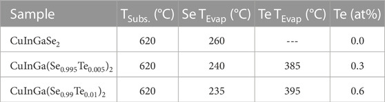
TABLE 1. Se and Te evaporation temperatures and Te concentrations of samples.
The CBD method was used for deposition of the CdS buffer layer. Cadmium acetate dihydrate (obtained from Alfa Aesar) with a purity of 99.999% was used as a cadmium source. Analytical grade (>99%) thiourea was obtained from Merck and was used as a sulfur source. In addition, 25% ammonia solution was obtained from Merck and was added as a complexing agent. The absorbers were dipped into the CBD solution and stirred at 15 rpm for 8 min at 60°C. The resulting CdS layer was approximately 50 nm thick. ZnO, ITO, and front contact depositions were performed using the Alliance Concept Eva 450 system with combined RF sputtering and e-beam evaporation. The purity of the ZnO and ITO targets was 99.99%. Non-doped ZnO and ITO layers were deposited by sputtering with thicknesses of approximately 100 nm and 200 nm, respectively. The Ni/Al/Ni front contact was added by e-beam evaporation. The thicknesses of the layers were 30 nm, 2 µm, and 30 nm for Ni, Al, and Ni, respectively. Al was obtained from Umicore with a purity of 99.999%; the purity of the Ni source was 99.95%.
A ZEISS Supra 40 VP scanning electron microscope (SEM) was used to evaluate the microstructure, with acceleration voltage set to 5 kV. Microstructure photographs were taken after absorber deposition. The chemical compositions of samples were determined using a Bruker EDS with acceleration voltage set to 15 kV; this was attached to the SEM. X-ray diffraction (XRD) analysis was carried out using a Rigaku MiniFlex 600 XRD with Cu–Kα radiation at 2θ values between 20° and 90°. Each absorber layer was also produced on SLG without a Mo back contact to eliminate the Mo peaks in XRD measurements and to enable investigation of the optical properties of the films. Absorbance measurements were carried out at wavelengths between 600 and 1,400 nm using a Shimadzu UV-2600 UV–Vis spectrophotometer. Time-resolved photoluminescence (TRPL) characterization was carried out after absorber layer deposition in order to understand the back contact recombination rate and to estimate the lifetime of the minority carriers. Glow discharge optical emission spectroscopy (GDOES) measurements were obtained using a Spectruma GDA750 to investigate the compositional depth profile. J-V measurements were performed under AM1.5G standard test conditions using a four-point measurement setup at room temperature. The lock-in method was employed to measure external quantum efficiency (EQE) using a xenon lamp equipped with a monochromator. Voc and FF values were obtained from the J-V results. Jsc was calculated via integration of the EQE result with the AM1.5G spectrum.
Figure 1 shows top-view and cross-sectional SEM images of the absorber thin films fabricated via a three-stage co-evaporation method. It can be seen in Figures 1A–C that all absorber layers were uniform, dense, and compact. However, the surface was rougher with incorporation of Te, which may have been caused by large grain formation. All absorber layers exhibited large columnar grains, and the thicknesses were approximately 2 μm in each case, as shown in Figures 1D–F. It appears that larger grains (up to 2 μm) were formed with incorporation of Te into the control film, implying that Te assisted in grain growth. The underlying reason is that Te crystallizes slowly due to its high boiling point, and therefore slower nucleation occurs during the three-stage process as a result of the higher diffusion rate of the Te compared to Se (Kwon and Hyeon, 2008; Gulen et al., 2018; Shukla et al., 2021). The larger grain size growth with incorporation of Te prevents the formation of disorder in grain boundaries (GBs) at the absorber/CdS interface and within the absorber layer, leading to higher Voc and FF; in addition, it would be more favorable for charge extraction and transfer to balance the length of charge carrier diffusion, resulting in higher Jsc (Xing et al., 2013; Yin et al., 2015).
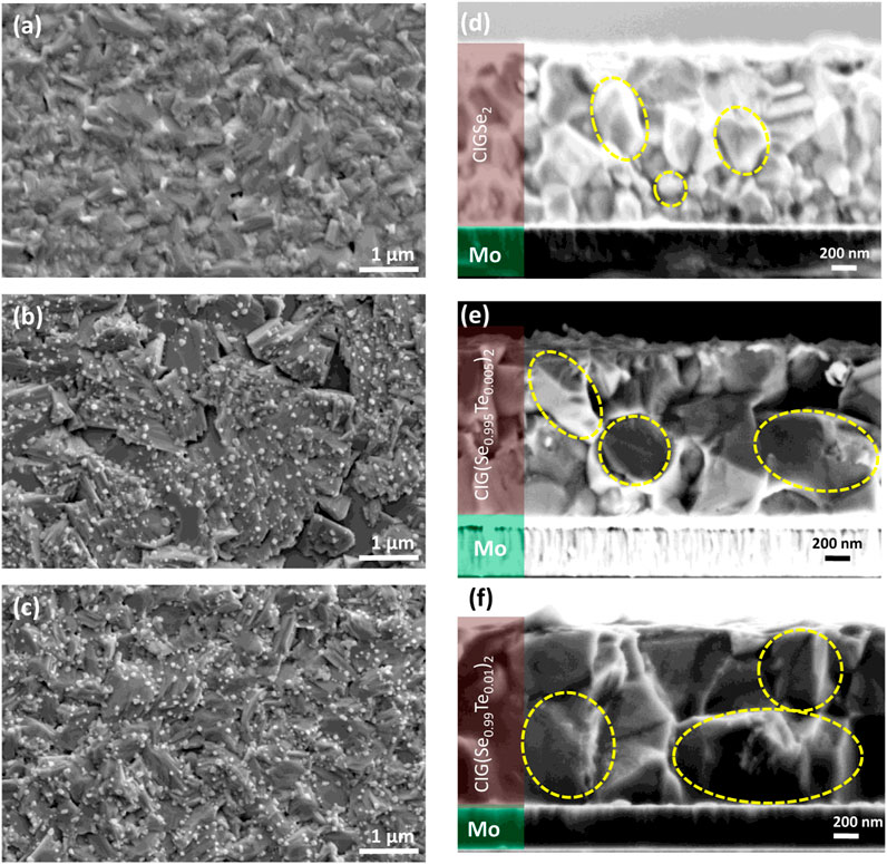
FIGURE 1. Top-view SEM images of the absorber layer in (A) the control without Te, (B) Cu(In,Ga)(Se0.995Te0.005)2-based thin film, and (C) Cu(In,Ga)(Se0.99Te0.01)2-based thin film (all scale bars 1 µm). Representative cross-sectional SEM view of (D) the control without Te, (E) Cu(In,Ga)(Se0.995Te0.005)2-based thin film, and (F) Cu(In,Ga)(Se0.99Te0.01)2-based thin film. (Yellow dotted lines in the inset images show grain size; all scale bars 200 nm.)
Figure 2A shows the XRD patterns of the absorber thin films with varying Te dopants grown on SLG via the three-stage process. The three dominant peaks related to the Cu(In,Ga)Se2 chalcopyrite phase, during which 0.3 GGI (JCPDS 00-035-1102) appeared in the XRD patterns with peaks of (112), (220/204), and (312/116). It can clearly be seen that the intensity of the (112) peak became weaker compared to that of the control absorber thin films; conversely, the intensities of the (220/204) and (312/116) peaks became stronger, which means that crystallization quality and orientation can be tuned through the incorporation of Te+2 anions during the three-stage co-evaporation process. In particular, the increase along the (220/204) and (312/116) orientations is regarded as the favorable crystallographic direction, because this is beneficial for carrier transportation and achieving a low density of non-radiative recombination centers in the Cu(In,Ga)Se2 absorber layer, leading to improvement in the charge transport mechanism in TFSCs (Contreras et al., 2006; Siebentritt et al., 2006). As expected, a reasonably strong shift in the strong (112) peak toward the lower angle was observed with an increase in Te dopants in the absorber thin film, as shown in Figure 2B. This is because of the greater ionic radii of Te2− (221 pm) anions in comparison to Se2− (198 pm) ions, which can lead to induction of stress and increase in the lattice parameters, suggesting that Te2− anions are replaced by Se2− and act as an interstitial impurity inside the thin film (Atasoy et al., 2018). The optical bandgap (Eg) of the absorber thin films with and without Te dopants was calculated by extrapolating the linear range to the energy axis in plots of (αhν)2 against energy, shown in Figure 2C. The bandgaps of the Cu(In,Ga)Se2, Cu(In,Ga)(Se0.995Te0.005)2, and Cu(In,Ga)(Se0.99Te0.01)2 thin films were determined to be 1.40, 1.39, and 1.38 eV, respectively, which would enable more efficient harvesting of solar energy according to the S-Q limit. No significant change was observed in the bandgap value with the incorporation of Te dopant at a low level. A negligible reduction in bandgap can be attributed to the difference between Se and Te chalcogenides in terms of Pauling electronegativity, which leads to an upshift in the band valence (Pauling, 1960). To gain insight into the charge transfer mechanism, we evaluated the hole-extraction ability by examining time-resolved photoluminescence (TRPL) spectra, shown in Figure 2D. As evident from Figure 2D, Cu(In,Ga)(Se0.99Te0.01)2 exhibited the lowest charge lifetime (1.4 ns), as compared to the Cu(In,Ga)(Se0.995Te0.005)2 (2 ns) and control (16 ns) thin films, considering that more PL quenching shows effective hole-extraction across the interface between the absorber and CdS. This can be explained by the reduction of defects in the GBs resulting from the larger grain sizes, consistent with SEM images (Jehl-Li-Kao et al., 2013). Considering these insights, we can surmise that Cu(In,Ga)(Se0.99Te0.01)2 exhibits greater hole-extraction efficiency than that of other options.
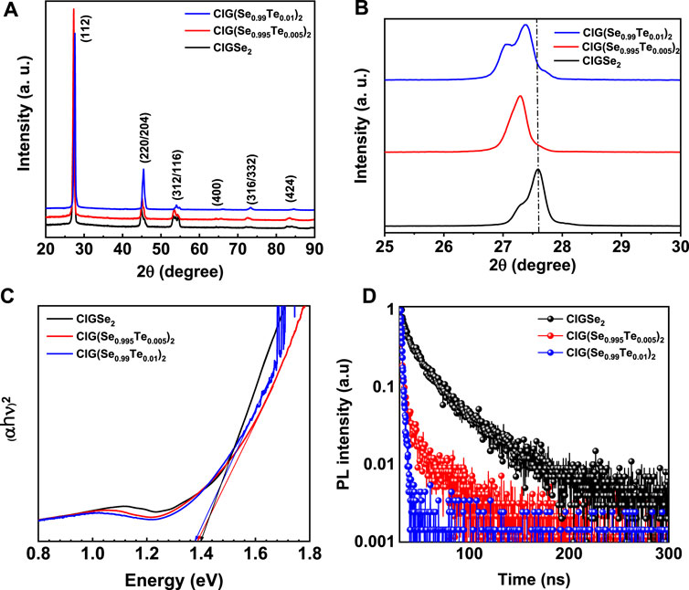
FIGURE 2. (A) XRD spectra of absorber thin films with varying Te dopants on SLG without Mo back contact. (B) Dominant orientation peak (112), illustrating peak broadening. (C) Tau plots for direct bandgap absorber thin films. (D) Time-resolved PL decay kinetics of absorber thin films with and without Te dopants.
Figure 3A shows the effects of the Te dopant on the GGI gradient of absorber thin films. The left side of the graph represents the absorber surface, and the right side represents the Mo back contact. The GGI gradient of control thin films resembled a typical three-stage co-evaporation gradient, with higher Ga content near the surface and the back contact (Jarzembowski et al., 2015; Schneider et al., 2021). Despite the evaporation of Ga at all stages, the presence of less Ga in the middle region can be explained by insufficient diffusion. When the notch in the middle region is too deep, it affects electron transition and increases the recombination rate (Zahedi-Azad et al., 2020). The addition of Te eliminated the notch in the middle region, as his improved the diffusion of Ga by increasing crystal quality. Figure 3A demonstrates that the Te-poor dopant caused a significant change in the GGI gradients. Although the GGI gradients of Te-doped and non-doped thin films differed markedly, the GGI gradients of both Te-doped thin films were similar. To gain insight into the impact of Te2− anions on the distribution of alkali elements (both sodium (Na) diffused from the substrate and rubidium (Rb) exposed by using post-deposition treatment (PDT)) we examined Na and Rb distributions in absorber thin films with varying Te dopant contents. The Na distributions of control and Cu(In,Ga)(Se0.99Te0.01)2 thin films were similar, and there was a slight increase in the region close to the back contact, as shown in Figure 3B. Since Na was not added from the surface, we speculate that the peak near the surface region in the case of the control thin films was caused by a measurement error. The amount of Na was higher in the region close to the back contact for all absorber thin films because Na diffuses from the substrate. The Na distribution of Cu(In,Ga)(Se0.995Te0.005)2 differed from that of the other thin films in the region close to the back contact. Na was able to diffuse at a high rate up to the middle region of the Cu(In,Ga)(Se0.995Te0.005)2 thin films. It is known that the incorporation of a small amount of Na improves the efficiency of Cu(In,Ga)Se2-based solar cells by increasing the hole concentration and conductivity (Urbaniak et al., 2014). However, the addition of excess Na may cause the solar cell parameters to deteriorate. Jackson et al. (2016) showed that PDT of heavier alkalis such as Cs and Rb increases the efficiency of low-GGI Cu(In,Ga)Se2 solar cells by improving diode quality. In addition, other groups have revealed that RbF PDT increases Voc by reducing recombination (Avancini et al., 2017; Karki et al., 2018; Feurer et al., 2019). In another study, Zahedi-Azad et al. (2019) investigated the effect of these heavier alkalis on the performance of high-GGI wide-bandgap Cu(In,Ga)Se2 solar cells. They found that both alkali groups were beneficial for achieving higher solar cell efficiency. However, the performances of the solar cell with Rb were better than those of a solar cell with Cs. Therefore, we selected RbF for PDT in this work. Figure 3C illustrates the effect of Te dopants on Rb distribution. As can be seen from Figure 3C, all absorber layers exhibited a peak in the surface region (left-hand side) due to non-diffused residual Rb particles. When the Rb distributions of the thin films with and without Te dopants were compared, it was observed that Rb diffused much more successfully in the thin films with Te dopants. As we know that the effects of Na can be seen within the bulk and the surface of the absorber layer, Rb mainly affects the absorber/CdS interface (Nwakanma et al., 2021). The addition of alkalis improves solar cell efficiency by reducing interface recombination and increasing the incorporation of Cd into the absorber (Chirila et al., 2013; Pianezzi et al., 2014).
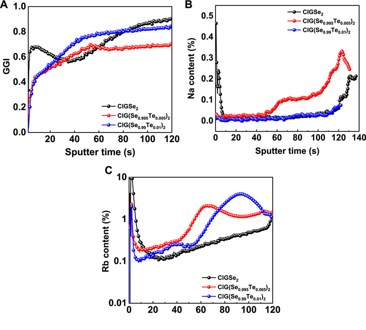
FIGURE 3. GGI gradients (A), Na distributions (B), and Rb distributions (C) for absorber thin films with varying Te dopant contents.
Figure 4A shows the photovoltaic performance of our best-performing cells with Cu(In,Ga)Se2, Cu(In,Ga)(Se0.995Te0.005)2, and Cu(In,Ga)(Se0.99Te0.01)2 thin films. As shown clearly in Table 2, both Te dopant-based devices exhibited lower Voc and higher Jsc values than the one based on the control film. The highest Jsc was obtained in the cell with Cu(In,Ga)(Se0.995Te0.005)2 thin film, and Jsc decreased with further increase of the Te dopant. This decrease may have originated from the high ideality factor, enhanced space charge region recombination, and low carrier collection as a result of the larger amount of Ga in the region close to the back contact (Orgis et al., 2013). Possible mechanisms underlying the enhanced device performance are the faster hole-extraction and transfer with reduction of parasitic optical losses, resulting in higher Jsc and additionally suppressing the defect in GBs through larger grain sizes, leading to higher FF (Dullweber et al., 2001; Gloeckler and Sites, 2005; Liu et al., 2020; Nwakanma et al., 2021). We observed kink effects in the J-V curves of the Cu(In,Ga)(Se0.995Te0.005)2 solar cell that may have been the reason for the lower FF. This kink in the current indicates potential barrier(s) to the majority carrier flow (injection barrier), which could be due to window/buffer band alignment or heavy accumulation of excess Na atoms at the interface or in front of the back contact (Weiss et al., 2018; Werner et al., 2018). In terms of overall evaluation, Te-poor TFSCs afforded an impressive efficiency of 9.58%, proving that a Te anion is a promising dopant for highly efficient wide-bandgap Cu(In,Ga)Se2 absorber-based solar cells. Figure 4B presents the EQE spectra of the best TFSCs between 350 and 1,050 nm. Both Te-incorporated thin films showed very high EQE curves compared to the control thin film, indicating negligible collection losses as a result of the very wide space charge region that is established for close-stoichiometric absorber compositions (Keller et al., 2021). In addition, the decrease in EQE values toward short wavelengths for the control thin -films was caused by reflection losses, providing evidence that a Te anion reduces reflection losses. Beyond this, we evaluated Voc and efficiency as a function of bandgap for Te-incorporated narrow- and wide-bandgap thin-film-based solar cells that have been reported in the literature in relation to this work. Figure 4C shows Voc as a function of bandgap (Eg) for previously reported solar cells based on narrow- and wide-bandgap chalcopyrite thin films. It is evident that Voc deficiency rapidly decreases with increasing bandgap; as expected, the highest Voc values were reached at bandgap values in the range 1.30–1.45 eV. The best Voc value was achieved at 1.38 eV bandgap in our recent work on Te-poor Cu(In,Ga)(Se,Te)2-based TFSCs. Figure 4D shows the corresponding values to provide a straightforward comparison of the efficiency achieved using different bandgap thin film absorbers. Figure 4D clearly shows that our cells based on Te-poor wide-bandgap absorbers exhibited better solar cell performance, achieving 9.58% efficiency, considerably higher than has previously been reported in the literature.
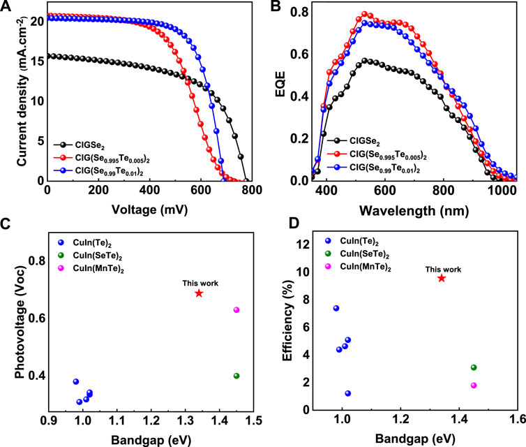
FIGURE 4. Photovoltaic performance of TFSCs using various absorber layers. (A) J–V curves, and (B) EQE of the best-performing devices. Summary of photovoltage and efficiency in the context of the literature: (C) photovoltage (Voc) versus bandgap (Eg); (D) efficiency versus bandgap (Eg) for tellurium-based TFSCs reported in the literature (Mise and Nakada, 2010a, Mise and Nakada, 2010b, Mise and Nakada, 2011; Jehl-Li-Kao et al., 2013; Kim et al., 2013; Hamid et al., 2019; Jia et al., 2019) and in the present article (the latter represented by red stars).
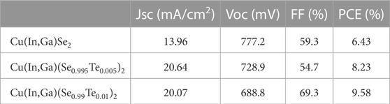
TABLE 2. Photovoltaic parameters of TFSCs.
We successfully prepared Te-poor CuInGa(SeTe)2 wide-bandgap absorbers using RbF PDT via a three-stage evaporation process and examined the impact of Te2− anions on photovoltaic performance in chalcopyrite solar cells. Absorber thin films incorporating Te exhibited effective hole-extraction, a considerable reduction in defects at the surface and grain boundary, lower carrier lifetime, and excellent crystal quality. Compared to control-based TFSCs (6.43%), Cu(In,Ga)(Se0.99Te0.01)2-based cells exhibited the highest efficiency, at 9.58%. Considering the previous reports in the literature, the Voc and efficiency values of 688 mV and 9.58%, respectively, in the 1.38 eV bandgap represent the highest achieved so far for wide-bandgap TFSCs incorporating Te2− anions. We foresee that future research directions could include the development of Te-based absorber materials with different cations and/or anions and with a device architecture designed with varied buffer layers and/or alkali-fluorine PDT to promote considerable efficiency and Voc for future wide-bandgap TFSCs.
The original contributions presented in the study are included in the article/Supplementary Material; further inquiries can be directed to the corresponding author.
SA: Investigation, Methodology, Visualization, Formal analysis, Writing – original draft; GÇ: Supervision, Conceptualization, Funding acquisition, and SS: Project administration, Visualization, Formal analysis, Writing – review and editing. All authors reviewed the article and approved the final version.
This work was supported by the Scientific and Technological Research Council of Turkey (TUBITAK 2211-C and 2214-A) and the Federal Ministry of Education and Research of Germany (Grant Number: 0324297B).
The authors declare that the research was conducted in the absence of any commercial or financial relationships that could be construed as a potential conflict of interest.
All claims expressed in this article are solely those of the authors and do not necessarily represent those of their affiliated organizations, or those of the publisher, the editors, and the reviewers. Any product that may be evaluated in this article, or claim that may be made by its manufacturer, is not guaranteed or endorsed by the publisher.
The Supplementary Material for this article can be found online at: https://www.frontiersin.org/articles/10.3389/fenrg.2023.1215712/full#supplementary-material
Akin, S., Erol, E., and Sonmezoglu, S. (2017). Enhancing the electron transfer and band potential tuning with long-term stability of ZnO based dye-sensitized solar cells by gallium and tellurium as dual-doping. Electrochim. Acta 225, 243–254. doi:10.1016/j.electacta.2016.12.122
Atasoy, Y., Başol, B. M., Olgar, M. A., Tomakin, M., and Bacaksız, E. (2018). Cu(In,Ga)(Se,Te)2 films formed on metal foil substrates by a two-stage process employing electrodeposition and evaporation. Thin Solid Films 649, 30–37. doi:10.1016/j.tsf.2018.01.025
Avancini, E., Carron, R., Weiss, T. P., Andres, C., Bürki, M., Schreiner, C., et al. (2017). Effects of rubidium fluoride and potassium fluoride postdeposition treatments on Cu(In,Ga)Se2 thin films and solar cell performance. Chem. Mat. 29, 9695–9704. doi:10.1021/acs.chemmater.7b03412
Beyer, W., Mell, H., and Stuke, J. (1971). Conductivity and thermoelectric power of trigonal SexTe1-x single crystals. Phys. Status Solidi B 45, 153–162. doi:10.1002/pssb.2220450116
Caldwell, R. S., and Fan, H. Y. (1959). Optical properties of tellurium and selenium. Phys. Rev. 114, 664–675. doi:10.1103/physrev.114.664
Chirila, A., Reinhard, P., Pianezzi, F., Bloesch, P., Uhl, A. R., Fella, C., et al. (2013). Potassium-induced surface modification of Cu(In,Ga)Se2 thin films for high-efficiency solar cells. Nat. Mat. 12, 1107–1111. doi:10.1038/nmat3789
Contreras, M. A., Romero, M. J., and Noufi, R. (2006). Characterization of Cu(In,Ga)Se2 materials used in record performance solar cells. Thin Solid Films 511, 51–54. doi:10.1016/j.tsf.2005.11.097
Dullweber, T. H., Hanna, G., Rau, U., and Schock, H. W. (2001). A new approach to high-efficiency solar cells by band gap grading in Cu(In,Ga)Se2 chalcopyrite semiconductors. Sol. Energy Mat. Sol. Cells 67, 145–150. doi:10.1016/s0927-0248(00)00274-9
Feurer, T., Fu, F., Weiss, T. P., Avancini, E., Löckinger, J., Buecheler, S., et al. (2019). RbF post deposition treatment for narrow bandgap Cu(In,Ga)Se2 solar cells. Thin Solid Films 670, 34–40. doi:10.1016/j.tsf.2018.12.003
Fiat, S., Bacaksiz, E., Kompitsas, M., and Çankaya, G. (2014a). Temperature and tellurium (Te) dependence of electrical characterization and surface properties for a chalcopyrite structured Schottky barrier diode. J. Alloys Compd. 585, 178–184. doi:10.1016/j.jallcom.2013.09.123
Fiat, S., Koralli, P., Bacaksiz, E., Giannakopoulos, K. P., Kompitsas, M., Manolakos, D. E., et al. (2013a). The influence of stoichiometry and annealing temperature on the properties of CuIn0.7Ga0.3Se2 and CuIn0.7Ga0.3Te2 thin films. Thin Solid Films 545, 64–70. doi:10.1016/j.tsf.2013.07.032
Fiat, S., Polat, I., Bacaksiz, E., Çankaya, G., Koralli, P., Manolakos, D. E., et al. (2014b). Optical and structural properties of nanostructured CuIn0.7Ga0.3(Se(1−x)Tex)2 chalcopyrite thin films—effect of stoichiometry and annealing. J. Nanosci. Nanotechnol. 14, 5002–5010. doi:10.1166/jnn.2014.8887
Fiat, S., Polat, I., Bacaksiz, E., Kompitsas, M., and Çankaya, G. (2013b). The influence of annealing temperature and tellurium (Te) on electrical and dielectrical properties of Al/p-CIGSeTe/Mo Schottky diodes. Curr. Appl. Phys. 13, 1112–1118. doi:10.1016/j.cap.2013.03.006
Gloeckler, M., and Sites, J. R. (2005). Band-gap grading in Cu(In,Ga)Se2 solar cells. J. Phys. Chem. Solids 66, 1891–1894. doi:10.1016/j.jpcs.2005.09.087
Guillemoles, J. F. (2002). The puzzle of Cu(In,Ga)Se2 (CIGS) solar cells stability. Thin Solid Films 403-404, 405–409. doi:10.1016/s0040-6090(01)01519-x
Gulen, M., Sarilmaz, A., Patir, I. H., Ozel, F., and Sonmezoglu, S. (2018). Ternary copper-tungsten-disulfide nanocube inks as catalyst for highly efficient dye-sensitized solar cells. Electrochim. Acta 269, 119–127. doi:10.1016/j.electacta.2018.02.137
Hamid, M., Fadaam, S. A., Mohammed, L. A., and Hussein, B. H. (2019). Influence of addition (Mn) on enhance efficiency of (CuInTe2) photovoltaic cell. Eurasian Chem. Technol. J. 21, 183–185.
Ishizuka, S., Taguchi, N., Nishinaga, J., Kamikawa, Y., Tanaka, S., and Shibata, H. (2018). Group III elemental composition dependence of RbF postdeposition treatment effects on Cu(In,Ga)Se2 thin films and solar cells. J. Phys. Chem. C 122, 3809–3817. doi:10.1021/acs.jpcc.8b00079
Jackson, P., Wuerz, R., Hariskos, D., Lotter, E., Witte, W., and Powalla, M. (2016). Effects of heavy alkali elements in Cu(In,Ga)Se2 solar cells with efficiencies up to 22.6. Phys. Status Solidi RRL 10, 583–586. doi:10.1002/pssr.201600199
Jarzembowski, E., Maiberg, M., Obereigner, F., Kaufmann, K., Krause, S., and Scheer, R. (2015). Optical and electrical characterization of Cu(In,Ga)Se2 thin film solar cells with varied absorber layer thickness. Thin Solid Films 576, 75–80. doi:10.1016/j.tsf.2015.01.004
Jehl-Li-Kao, Z., Kobayashi, T., and Nakada, T. (2013). CuIn(Se1−xTex)2 solar cells with tunable narrow-bandgap for bottom cell application in multijunction photovoltaic devices. Sol. Energy Mat. Sol. Cells 119, 144–148. doi:10.1016/j.solmat.2013.05.054
Jia, G., Liu, B., Wang, K., Wang, C., Yang, P., Liu, J., et al. (2019). CuInTe2 nanocrystals: Shape and size control, formation mechanism and application, and use as photovoltaics. Nanomaterials 9, 409. doi:10.3390/nano9030409
Ju, M. G., Dai, J., Ma, L., and Zeng, X. C. (2017). Perovskite chalcogenides with optimal bandgap and desired optical absorption for photovoltaic devices. Adv. Energy Mat. 7, 1700216. doi:10.1002/aenm.201700216
Kamikawa, Y., Masuda, T., Nishinaga, J., and Ishizuka, S. (2022). Influence of argon pressure on sputter-deposited molybdenum back contacts for flexible Cu(In,Ga)Se2 solar cells on polyimide films. Sol. Energy 241, 327–334. doi:10.1016/j.solener.2022.06.006
Karatay, A., Küçüköz, B., Çankaya, G., Ateş, A., and Elmali, A. (2017). The effect of Se/Te ratio on transient absorption behavior and nonlinear absorption properties of CuIn0.7Ga0.3(Se1−xTex)2 (0 ≤ x ≤ 1) amorphous semiconductor thin films. Opt. Mat. 73, 20–24. doi:10.1016/j.optmat.2017.07.046
Karki, S., Paul, P., Rajan, G., Belfore, B., Poudel, D., Rockett, A., et al. (2018). Analysis of recombination mechanisms in RbF-treated CIGS solar cells. IEEE J. Photovoltaics 9, 313–318. doi:10.1109/jphotov.2018.2877596
Kaya, I. C., Ozdemir, R., Usta, H., and Sonmezoglu, S. (2022). A dopant-free 2,7-dioctyl[1]benzothieno[3,2-b] [1]benzothiophene (C8-BTBT)-based hole transporting layer for highly stable perovskite solar cells with efficiency over 22%. J. Mat. Chem. A 10, 12464–12472. doi:10.1039/d2ta01541b
Keller, J., Pearson, P., Shariati Nilsson, N., Stolt, O., Stolt, L., and Edoff, M. (2021). Performance limitations of wide-gap (Ag,Cu)(In,Ga)Se2 thin-film solar cells. Sol. RRL 5, 2100403. doi:10.1002/solr.202100403
Kim, K., Hanket, G. M., Huynh, T., and Shafarman, W. N. (2012). Three-step H2Se/Ar/H2S reaction of Cu-In-Ga precursors for controlled composition and adhesion of Cu(In,Ga)(Se,S)2 thin films. J. Appl. Phys. 111, 083710. doi:10.1063/1.4704390
Kim, S., Kang, M., Kim, S., Heo, J. H., Noh, J. H., Im, S. H., et al. (2013). Fabrication of CuInTe2 and CuInTe2–xSex ternary gradient quantum dots and their application to solar cells. ACS Nano 7, 4756–4763. doi:10.1021/nn401274e
Kobayashi, T., Yamaguchi, H., Jehl Li Kao, Z., Sugimoto, H., Kato, T., Hakuma, H., et al. (2015). Impacts of surface sulfurization on Cu(In1−x,Gax)Se2 thin-film solar cells. Prog. Photovoltaics Res. Appl. 23, 1367–1374. doi:10.1002/pip.2554
Kwon, S. G., and Hyeon, T. (2008). Colloidal chemical synthesis and formation kinetics of uniformly sized nanocrystals of metals, oxides, and chalcogenides. Acc. Chem. Res. 41, 1696–1709. doi:10.1021/ar8000537
Liu, F., Zeng, Q., Li, J., Hao, X., Ho-Baillie, A., Tang, J., et al. (2020). Emerging inorganic compound thin film photovoltaic materials: Progress, challenges and strategies. Mat. Today 41, 120–142. doi:10.1016/j.mattod.2020.09.002
Liu, W., Li, H., Qiao, B., Zhao, S., Xu, Z., and Song, D. (2022). Highly efficient CIGS solar cells based on a new CIGS bandgap gradient design characterized by numerical simulation. Sol. Energy 233, 337–344. doi:10.1016/j.solener.2022.01.054
Lundberg, O., Edoff, M., and Stolt, L. (2005). The effect of Ga-grading in CIGS thin film solar cells. Thin Solid Films 480-481, 520–525. doi:10.1016/j.tsf.2004.11.080
Mabvuer, F. T., Nya, F. T., and Kenfack, G. M. D. (2022). Improving the absorption spectrum and performance of CIGS solar cells by optimizing the stepped band gap profile of the multilayer absorber. Sol. Energy 240, 193–200. doi:10.1016/j.solener.2022.05.037
Madelung, O. (2012). Semiconductors: Data handbook. Berlin/Heidelberg: Springer Science & Business Media.
Mise, T., and Nakada, T. (2011). Effect of tellurium deposition rate on the properties of Cu–In–Te based thin films and solar cells. J. Cryst. Growth 314, 76–80. doi:10.1016/j.jcrysgro.2010.10.147
Mise, T., and Nakada, T. (2010a). Low temperature growth and properties of Cu–In–Te based thin films for narrow bandgap solar cells. Thin Solid Films 518, 5604–5609. doi:10.1016/j.tsf.2010.04.065
Mise, T., and Nakada, T. (2010b). Microstructural and optical properties of CuIn3Te5 thin films for solar cells. Sol. Energy Mat. Sol. Cells 94, 1132–1136. doi:10.1016/j.solmat.2010.02.050
Naghavi, N., Mollica, F., Goffard, J., Posada, J., Duchatelet, A., Jubault, M., et al. (2017). Ultrathin Cu(In,Ga)Se2 based solar cells. Thin Solid Films 633, 55–60. doi:10.1016/j.tsf.2016.11.029
NREL Best Research-Cell Efficiency Chart (2022). Research-cell efficiency Chart. Avaliable At: https://www.nrel.gov/pv/cell-efficiency.html ((accessed November, 2022).
Nwakanma, O., Subramaniam, V., and Morales-Acevedo, A. (2021). Review on the effects due to alkali metals on copper–indium–gallium–selenide solar cells. Mat. Today Energy 20, 100617. doi:10.1016/j.mtener.2020.100617
Oliveira, A. J. N., Teixeira, J. P., Ramos, D., Fernandes, P. A., and Salomé, P. M. P. (2022). Exploiting the optical limits of thin film solar cells: A review on light management strategies in Cu(in,Ga)Se2. Adv. Photonics Res. 3, 2100190. doi:10.1002/adpr.202100190
Orgis, T., Maiberg, M., and Scheer, R. (2013). Influence of band gradients on Cu(In,Ga)Se2 solar cell diode factors. J. Appl. Phys. 114, 214506. doi:10.1063/1.4840995
Pianezzi, F., Reinhard, P., Chirila, A., Bissig, B., Nishiwaki, S., Buecheler, S., et al. (2014). Unveiling the effects of post-deposition treatment with different alkaline elements on the electronic properties of CIGS thin film solar cells. Phys. Chem. Chem. Phys. 16, 8843–8851. doi:10.1039/c4cp00614c
Polman, A., Knight, M., Garnett, E. C., Ehrler, B., and Sinke, W. C. (2016). Photovoltaic materials: Present efficiencies and future challenges. Science 352, aad4424. doi:10.1126/science.aad4424
Rosenfield, R. E., Parthasarathy, R., and Dunitz, J. D. (1977). Directional preferences of nonbonded atomic contacts with divalent sulfur. 1. Electrophiles and nucleophiles. J. Am. Chem. Soc. 99, 4860–4862. doi:10.1021/ja00456a072
Scheer, R., Klenk, R., Klaer, J., and Luck, I. (2004). CuInS2 based thin film photovoltaics. Sol. Energy 77, 777–784. doi:10.1016/j.solener.2004.08.004
Schneider, T., Dethloff, C., Hölscher, T., Kempa, H., and Scheer, R. (2021). Comparison of Mo and ITO back contacts in CIGSe solar cells: Vanishing of the main capacitance step. Prog. Photovolt. Res. Appl. 30, 191–202. doi:10.1002/pip.3476
Shockley, W., and Queisser, H. J. (1961). Detailed balance limit of efficiency of p-n junction solar cells. J. Appl. Phys. 32, 510–519. doi:10.1063/1.1736034
Shukla, S., Sood, M., Adeleye, D., Peedle, S., Kusch, G., Dahliah, D., et al. (2021). Over 15% efficient wide-band-gap Cu(In,Ga)S2 solar cell: Suppressing bulk and interface recombination through composition engineering. Joule 5, 1816–1831. doi:10.1016/j.joule.2021.05.004
Siebentritt, S., Sadewasser, S., Wimmer, M., Leendertz, C., Eisenbarth, T., and Lux-Steiner, M. C. (2006). Evidence for a neutral grain boundary barrier in chalcopyrites. Phys. Rev. Lett. 97, 146601. doi:10.1103/physrevlett.97.146601
Sonmezoglu Ates, O., Akin, S., Terzi, B., Mutlu, S., and Sonmezoglu, S. (2016). An effective approach for high-efficiency photoelectrochemical solar cells by using bifunctional DNA molecules modified photoanode. Adv. Funct. Mat. 26, 8776–8783. doi:10.1002/adfm.201603454
Sonmezoglu, S., and Akman, E. (2014). Improvement of physical properties of ZnO thin films by tellurium doping. Appl. Surf. Sci. 318, 319–323. doi:10.1016/j.apsusc.2014.06.187
Sonmezoglu, S. (2014). Synthesis and characterisations of nanostructured TiO2-Te:CdO compound thin films. Mat. Technol. 29, 3–7. doi:10.1179/175355513x13649076812440
Sonmezoglu, S., Termeli, T. A., Akin, S., and Askeroglu, I. (2013). Synthesis and characterization of tellurium-doped CdO nanoparticles thin films by sol-gel method. J. Sol-Gel Sci. Technol. 67, 97–104. doi:10.1007/s10971-013-3054-1
Steinke, T., Engelage, E., and Huber, S. M. (2023). Chalcogen bonding in the solid-state structures of 1,3-bis(benzimidazoliumyl)benzene-based chalcogen-bonding donors. Acta Cryst. C 79, 26–35. doi:10.1107/s2053229622011536
Theelen, M., and Daume, F. (2016). Stability of Cu(in,Ga)Se2 solar cells: A literature review. Sol. Energy 133, 586–627. doi:10.1016/j.solener.2016.04.010
Urbaniak, A., Igalson, M., Pianezzi, F., Bücheler, S., Chirila, A., Reinhard, P., et al. (2014). Effects of Na incorporation on electrical properties of Cu(In,Ga)Se2-based photovoltaic devices on polyimide substrates. Sol. Energy Mat. Sol. Cells 128, 52–56. doi:10.1016/j.solmat.2014.05.009
Wei, S. H., Zhang, S. B., and Zunger, A. (1998). Effects of Ga addition to CuInSe2 on its electronic, structural, and defect properties. Appl. Phys. Lett. 72, 3199–3201. doi:10.1063/1.121548
Weiss, T. P., Nishiwaki, S., Bissig, B., Carron, R., Avancini, E., Löckinger, J., et al. (2018). Injection current barrier formation for RbF postdeposition-treated Cu(In,Ga)Se2-based solar cells. Adv. Mat. Interfaces 5, 1701007. doi:10.1002/admi.201701007
Werner, F., Wolter, M. H., Siebentritt, S., Sozzi, G., Di Napoli, S., Menozzi, R., et al. (2018). Alkali treatments of Cu(In,Ga)Se2 thin-film absorbers and their impact on transport barriers. Prog. Photovolt. Res. Appl. 26, 911–923. doi:10.1002/pip.3032
Witte, W., Abou-Ras, D., Albe, K., Bauer, G. H., Bertram, F., Boit, C., et al. (2015). Gallium gradients in Cu(In,Ga)Se2 thin-film solar cells. Prog. Photovolt. Res. Appl. 23, 717–733. doi:10.1002/pip.2485
Xing, G., Mathews, N., Sun, S., Lim, S. S., Lam, Y. M., Gratzel, M., et al. (2013). Long-range balanced electron-and hole-transport lengths in organic-inorganic CH3NH3PbI3. Science 342, 344–347. doi:10.1126/science.1243167
Yin, W. J., Chen, H., Shi, T., Wei, S. H., and Yan, Y. (2015). Origin of high electronic quality in structurally disordered CH3NH3PbI3 and the passivation effect of Cl and O at grain boundaries. Adv. Electron. Mat. 1, 1500044. doi:10.1002/aelm.201500044
Zahedi-Azad, S., Maiberg, M., Clausing, R., and Scheer, R. (2019). Influence of heavy alkali post deposition treatment on wide gap Cu(In,Ga)Se2. Thin Solid Films 669, 629–632. doi:10.1016/j.tsf.2018.11.041
Keywords: Cu(In,Ga)(Se,Te)2 solar cells, Te anions, RbF post-deposition treatment, three-stage co-evaporation, wide-bandgap chalcopyrite absorber thin-films, GGI gradient
Citation: Ağca S, Çankaya G and Sonmezoglu S (2023) Impact of tellurium as an anion dopant on the photovoltaic performance of wide-bandgap Cu(In,Ga)Se2 thin-film solar cells with rubidium fluoride post-deposition treatment. Front. Energy Res. 11:1215712. doi: 10.3389/fenrg.2023.1215712
Received: 02 May 2023; Accepted: 06 July 2023;
Published: 28 July 2023.
Edited by:
Runsheng Tang, Yunnan Normal University, ChinaReviewed by:
Sahil Tahiliani, Applied Materials, United StatesCopyright © 2023 Ağca, Çankaya and Sonmezoglu. This is an open-access article distributed under the terms of the Creative Commons Attribution License (CC BY). The use, distribution or reproduction in other forums is permitted, provided the original author(s) and the copyright owner(s) are credited and that the original publication in this journal is cited, in accordance with accepted academic practice. No use, distribution or reproduction is permitted which does not comply with these terms.
*Correspondence: S. Ağca, YWdjYXNlbWloQGdtYWlsLmNvbSYjeDAyMDBhOw==
Disclaimer: All claims expressed in this article are solely those of the authors and do not necessarily represent those of their affiliated organizations, or those of the publisher, the editors and the reviewers. Any product that may be evaluated in this article or claim that may be made by its manufacturer is not guaranteed or endorsed by the publisher.
Research integrity at Frontiers
Learn more about the work of our research integrity team to safeguard the quality of each article we publish.