 Xiaobo Li
 Wei Xi
 Yang Yu
95% of researchers rate our articles as excellent or good
Learn more about the work of our research integrity team to safeguard the quality of each article we publish.
Find out more
ORIGINAL RESEARCH article
Front. Energy Res. , 25 October 2023
Sec. Smart Grids
Volume 11 - 2023 | https://doi.org/10.3389/fenrg.2023.1105148
This article is part of the Research Topic Control and Protection Technologies in High Renewable Energy Penetrated Power System View all 4 articles
The relay protection device is the core equipment that ensures the safe and stable operation of a power grid. With the open access of a large number of distributed generation, DC transmission and electric vehicles, a new deep low-carbon power system dominated by power electronic devices has gradually been formed. It is difficult for the traditional control and protection architecture, methods, and technology to meet the business characteristics and functional requirements of a diversified interaction, agile response, safety, and credibility of the power grid in the future. This paper presents a chip-based relay protection technology based on system-on-chip (SoC), which is described from four aspects, namely, the architectural design of the relay protection SoC, software and hardware cooperative relay protection based on the SoC IP core, experimental verification, and engineering application. The results show that the relay protection SoC proposed in this paper has significantly improved the performance of high-speed data acquisition and interaction through hardware algorithm engine acceleration and software and hardware collaborative computing, which is helpful to realize the local equipment operation and the integration of primary and secondary equipment, shorten the protection action time, and improve the speed, reliability, and stability of relay protection devices.
Relay protection is the first line of defense for the safe operation of the power grid. It is the key technical means to ensure the stability of the power grid and the safety of power equipment, and the relay protection device is the core component of the relay protection.
The earliest relay protection is the fuse. When the electrical equipment or power supply line is short-circuited, the fault can be removed as the fuse melts because of the large short-circuit current. With the increase of power generation equipment capacity and the expansion of power supply range, in many cases, the use of fuses alone cannot meet the requirements of selectivity and sensitivity. Therefore, overcurrent relays that specifically act on current breaking devices (circuit breakers) appear. In the 1890s, electromagnetic overcurrent relays installed on circuit breakers and directly acting on circuit breakers appeared. At the beginning of the 20th century, with the development of the power system, relays began to be widely used in the protection of the power system. An electromechanical relay is the most important representative; it meets the requirements of relay protection for small- and medium-sized generators below 100 MW and power grids below 220 kV. This protection device is reliable and does not need additional power supply. It has good anti-interference performance and a long service time. However, the electromechanical relay protection device is composed of electromechanical relays with mechanical rotating parts with contact opening and closing. It has the disadvantages of large volume, large power consumption, slow action speed, easy wear or adhesion of mechanical rotating parts and contacts, and complex debugging and maintenance. It is difficult to meet the requirements of ultra-high voltage and large-capacity power systems for relay protection rapidity and sensitivity (Zhang, 2009).
In the early 1950s, with the development of semiconductor transistors, transistor relay protection devices began to appear. The core part of the transistor-type relay protection device is the transistor electronic circuit, which is mainly composed of a crystal triode, a diode, a resistor, a capacitor, and an inductor. However, components such as transistors are easily damaged and cause protection misoperation. At the same time, it has poor anti-interference performance and reliability that need to be improved. In the mid-1970s, an integrated circuit technology developed rapidly. It integrates hundreds or more transistors into a semiconductor chip, which is smaller and more reliable. Therefore, people began to study integrated circuit relay protection devices based on integrated operational amplifier circuits. With the development of the electronic computer technology, especially the application of a microcomputer and microprocessor, the research of computer relay protection has achieved remarkable results. The microcomputer relay protection device has become the main focus for researchers at home and abroad and is widely used in the power grid. Microcomputer relay protection is an intelligent piece of industrial control equipment, and the various chips and running software, as well as logic, constitute the core elements of microcomputer relay protection (Zhang, 2009). Compared with traditional electromagnetic, transistor, and integrated circuit relay protection devices, microcomputer relay protection stands out because of its functional diversity and hardware reliability. It has been deeply developed and has become the mainstream hardware equipment in relay protection devices.
At present, the application of a 32-bit microcontroller unit (MCU) and DSP is dominant in the microcomputer relay protection device. With the increase in power grid capacity and the substantial increase in the number of electrical equipment, in order to cover more electrical equipment and improve the reliability of the hardware, as well as avoid the misoperation of the relay protection device, microcomputer relay protection devices are evolved from a single CPU structure to a multi-CPU co-processing structure (Xi et al., 2017); the structure of the DSP is also developed from a single DSP structure to multiple DSP fusion processing structure and from a single CPU or DSP structure development to a CPU and DSP hybrid structure. There are three reasons why microcomputer relay protection develops so rapidly. First, the technical progress is promoted by the huge market demand brought by the expansion of power grid capacity. Second, in order to increase the redundancy of hardware equipment and achieve hardware self-test and mutual inspection, equipment reliability must be improved. Third, with the continuous application of various algorithms and theories, the processor performance of the microcomputer relay protection device has higher requirements (Liu and Cai, 2014).
The application of a single-chip microcomputer and DSP has significantly improved the reliability and performance of the microcomputer relay protection device, but there are still some shortcomings. First, the performance is still insufficient. The MCU adopts the method of executing instructions one by one to complete various computing and logical functions, so its performance is naturally limited. Second, the MCU must be initialized at the beginning of the work, which has certain requirements for the level and timing. Although there are numerous reset circuits, its reliability has not been fundamentally improved. Finally, multi-CPU/DSP architecture also allows for additional internal hardware interfaces, while it causes significant inconvenience to the development and debugging of the hardware, as the engineers who develop and debug the hardware should not only consider the development of each module but also consider the interconnection between chips (Chen et al., 2017).
With a large number of distributed power sources, DC transmission, and electric vehicles being open to the power system, the power system gradually evolves into a deep low-carbon new power system dominated by power electronic devices. Compared to electromagnetic devices, the ability of power electronic devices to withstand fault current is much weaker, and a very short duration of fault current can permanently damage power electronic devices. Therefore, the protection device needs to act fast enough, and the rapidity of the protection device mainly depends on its basic components (overcurrent relay of the electromechanical protection device, CMOS circuit of the integrated circuit relay protection device, software program of the microcomputer relay protection device, etc.). The basic components of the existing microcomputer protection device realize the power algorithm or relay function through the software program. The rapidity of the basic components depends on the software program logic. In addition, the execution of the domestic software program generally adopts the serial mode, and the protection response time can only reach the millisecond level, which does not meet the speed requirements of the microsecond protection control of the new power system under the high power electronic permeability in the future. In view of the aforementioned technical problems, under the background of rapid development of the integrated circuit technology, chip protection has been spawned (Ye, 2021). Chip protection uses a field-programmable gate array (FPGA) to replace the CPU in the previous multi-core architecture, and designers can use its reconfigurable characteristics to implement multiple protection modules (Wu et al., 2019; Li et al., 2009). By integrating various intellectual property (IP) cores into the FPGA, a system-on-chip with complex functions and high reliability can be realized. System-on-chip (SoC)-based relay protection integrates the core function of the whole microcomputer relay protection system into one chip. The SoC replaces the multi-board and multi-chip architecture of the original device, which can realize data processing, digital interface, protection logic calculation and judgment and can realize device communication management, chip internal data sharing, etc. (Li et al., 2009).
Obviously, multiple chips are integrated into the same chip, and multiple chips are used for combinatorial logic optimization configuration to realize the serial execution of the basic components of the protection device to parallel processing, speed up the action speed of the basic components, and then, improve the protection speed. Therefore, the integration of multiple chips to achieve a system-on-chip is the main developmental trend of microcomputer relay protection in the future. The contributions of this paper are as follows:
1) A chip relay protection technology based on system-on-chip is proposed, and the SoC architecture of the relay protection device based on the system-on-chip is designed. A hardware and software cooperative relay protection algorithm based on the system-on-chip IP core is proposed.
2) Extensive experiments and field engineering demonstration analysis are carried out. Compared to the microcomputer protection device, the relay protection SoC architecture and hardware and software collaborative protection algorithms proposed in this paper replace the existing complex board-level multi-chip architecture. Through hardware algorithm engine acceleration and hardware and software collaborative computing, the performance of high-speed data acquisition and interaction is significantly improved.
The chip of SoC-based relay protection is a system-level chip of the microcomputer relay protection device, which contains the complete system of the microcomputer relay protection device and all contents of embedded software, and is the core unit of the microcomputer relay protection device. The SoC here refers to a product, an integrated circuit with specific goals and purposes. In a narrow sense, the relay protection SoC is the core chip integration of the microcomputer relay protection device, which integrates the key components of the whole microcomputer relay protection system into one chip. In a broad sense, the relay protection SoC is a micro system, which not only contains the CPU but also an A/D converter, D/A converter, communication chip, digital signal processor (DSP), and other hardware.
The overall architecture of the relay protection SoC is shown in Figure 1, which usually includes the following parts:
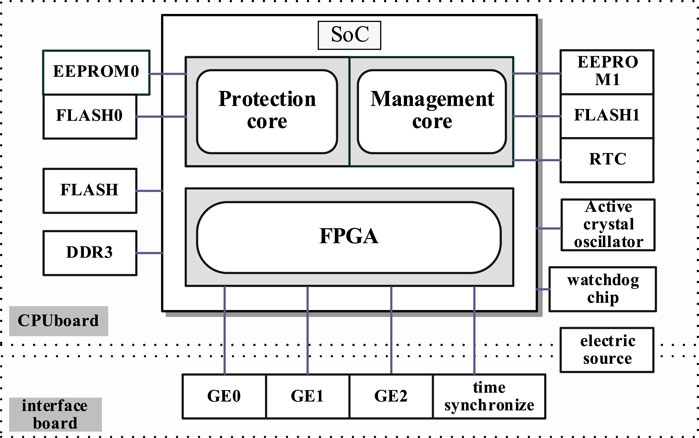
FIGURE 1. Overall architecture of the SoC for relay protection of a power system. (1) CPU: The CPU is the core of the calculation and control of the relay protection system, as well as the final execution unit of information processing and program operation of the protection system. The early microcomputer relay protection device used an 8-bit CPU, and the current mainstream uses a 32-bit CPU. (2) FPGA: The FPGA is a programmable logic array, which is a semi-customized circuit. The relay protection SoC usually uses a relatively small FPGA, which is convenient for processing the data stream (data communication, filtering, etc.) of the chip. The reconfigurable characteristics of the FPGA are utilized to integrate various IP cores into the FPGA, so as to construct a system on the chip with complex functions and high reliability (Xi et al., 2016). (3) Bus: The bus is a public communication trunk line that transmits information between each module of the relay protection SoC and comprises wires. According to functions and specifications, buses can be divided into five types, namely, data bus, address bus, control bus, extension bus, and local bus. With the continuous improvement of the complexity and integration of the relay protection SoC, a properly designed bus can reduce the impact caused by the communication delay of on-chip interconnections, thus improving the overall performance of the system-on-chip (Cao and Huang, 2014). (4) Memory: Generally speaking, the relay protection SoC contains high-speed buffer memory and static random-access memory (SRAM). Because the access speed of the main memory is much slower than the operating speed of the central processing unit, the high-speed processing capacity of the central processing unit cannot be given full access, and then, the working efficiency of the whole computer system is affected. The high-speed buffer memory is designed to solve this problem.
The internal structure of the relay protection SoC includes a processor system (PS) and programmable logic (PL). The PS part of the chip is a dual-core processor, which is run independently by two CPU cores, called protection core and management core. Each core can implement the functions that previously required a single board. Therefore, the “CPU board” and “management board” in the traditional digital relay protection device can use two cores in the SoC to achieve the corresponding functions.
The protection core is based on a bare metal (BM) mode that without the participation of the operating system, it replaces the “CPU board” in the traditional digital relay protection device. In the protection core, protection functions and basic services with high real-time requirements need to be implemented.
The application software of a protection core mainly carries out three parts of business functions, namely, the main program, sampling interrupt service program, and fault handling interrupt program.
In normal, the main program is run to complete the functions, including the hardware self-test, casting and cutting platen, curing and setting values, and sending reports. The sampling interrupt procedure is executed every other sampling interval to collect the electrical volume, record the wave, and distinguish the sudden variable start-up. The fault handling interrupt procedure is also executed every fixed time to complete the protection function logic and the abnormal judgment of PT (potential transformer) and CT (current transformer). If any exception occurs, corresponding alarm signals and packets are sent.
For common alarms (abnormal operation protection), sending a signal to remind the operator to pay attention to check and handle; for serious alarms (device failure) that endanger the safety and reliability of the protection, the protection outlet is locked while sending out the signal.
When a failure occurs in the power system, the corresponding protection function is completed in the fault handling the interrupt program until the whole group is reset and returns to the normal operation of the main program.
In the protection core, a set of driver interfaces for invoking hardware resources are designed for the protection application software of the device. The memory management function is provided through the system function to ensure the normal operation of each functional logic of the application software. All time information of the chip is managed uniformly according to the external B code or 1588 time synchronization message to provide external time information for each business function of the protection and management cores.
A management core based on a customized Linux operating system improves efficiency and simplifies key operations, such as memory allocation and other links. The core mainly completes the IEC 61850 protocol, measurement, and control and management functions to replace the traditional digital relay protection device in the “management board.”
The driver portion of the management core needs to be able to support the related functions and basic dependencies of the customized Linux operating system. The driver part of the management core has the basic serial port, network port, and flash read and write drivers. It can automatically load the Linux kernel image and the root file system. Meanwhile, it supports parameter configuration and storage functions and can flexibly select the Linux kernel loading mode (Chen et al., 2007).
The management communication software of the management core is responsible for the interaction and management of the configuration and data of the protection measurement and control system, as well as providing the corresponding light alarms, and communicating with the background through the IEC 61850 communication protocol. The management communication software adopts the C/S architecture, which can be flexibly deployed according to the specific product design in practical applications. It can be deployed on the same board or to different boards, making the whole system more flexible. Data in management communication software can be divided into operation information, real-time data, resource data, and historical report data.
The programmable logic (PL) portion of the chip is the FPGA portion. By using the reconfigurable feature of the FPGA, multiple protection algorithm modules can be integrated into one protection function-integrated circuit module in a pre-programmed way. Such a pre-designed and certified reusable integrated circuit module is commonly referred to as an intellectual property (IP) core (Graham et al., 2013).
The whole process of relay protection calculation and processing includes data sampling value processing, electrical parameter calculation, logic judgment, network communication, and other links, involving a front-end data processing class algorithm, electrical parameter calculation algorithm, data management algorithm, and network communication algorithm. Among these algorithms, electrical parameter calculation algorithm and data management algorithm are easy to change with the change of product demand, which is suitable to be realized by a special DSP with better software programmability, while the front-end data processing class algorithm has higher requirements on processing performance; the network communication algorithm is constrained by standard specifications, and the demand is relatively fixed. Therefore, these two kinds of algorithms are suitable for IP core hardware implementation (Yang et al., 2020).
Figure 2 shows the layout of the power-specific algorithm IP core in the relay protection SoC.
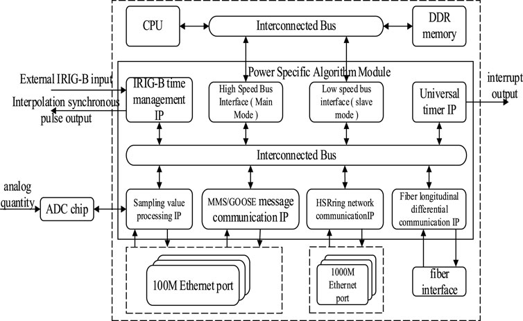
FIGURE 2. Flowchart of the thunderstorm trend prediction algorithm.
Among them, the sampling value processing IP control external ADC chip was used to collect analog voltage and current and is responsible for organizing SV messages; the GOOSE/MMS message communication IP is responsible for GOOSE and MMS message sending, receiving, and filtering; the sampling value processing IP and GOOSE/MMS message communication IP are connected to the 100 Mbit/s Ethernet network port for communication between the process layer, the interval layer, and the process layer and the interval layer intelligent devices; the hierarchical state routing (HSR) ring communication IP is responsible for receiving and filtering messages between the process layer and interval layer intelligent devices in the same interval and is connected to gigabit Ethernet network ports. Second, there are built-in universal timer IP and IRIG-B time management IP in the power dedicated algorithm module. The former is responsible for output interruption and the latter is responsible for time. The optical fiber longitudinal differential communication IP can provide a physical communication link and connect with the optical fiber interface to be responsible for clock synchronization and cache control of intelligent devices between the process layer and the interval layer. Third, the data management IP is responsible for the compression and verification of message data to reduce the network transmission bandwidth requirements. Finally, the communication interface between the power-specific algorithm module and the CPU includes the high-speed bus interface and the low-speed bus interface. On the one hand, the low-speed bus interface works in the slave mode and is controlled by the CPU master. It is used by the CPU to configure the internal registers of the power-specific algorithm module and carry out small data transfer. On the other hand, the high-speed bus interface works in the main mode and the power-dedicated algorithm module is the main control terminal, which can directly read and write the double data rate (DDR) memory on the CPU side. It is mainly used for a large amount of data movement, such as sampling value messages and GOOSE and MMS messages received from the external network port.
The SoC relay protection adopts the advanced expandable interface (AEI), bus, in the advanced microcontroller bus architecture (AMBA) to realize the interconnection of subsystems on the chip. The chip adopts a high-performance dual-core CK860 processor with an AEI bus interface, so each CPU core can directly be connected to the power dedicated algorithm IP core with standard AEIs and the system SRAM storage unit. Due to the use of high-performance AEI bus to connect the CPU core, storage unit, and ASIC, its security and transmission rate are much higher than that of non-SoC on-board the transmission scheme, and the data bandwidth can reach the level of 3–5 Gbit/s, which is an order of magnitude higher than the general processor and FPGA architecture. In addition, the information communication between cores can be realized with the interrupt mechanism.
The SoC for on-chip relay protection can carry out hardware-based high-speed processing of specific data or signals by customizing different types of functional units based on integrated circuits into IP core modules, thus realizing the serial execution to parallel processing of protection devices’ basic components, speeding up the action speed of basic components, and improving the protection rapidness. It meets the new power system to protect the basic components of higher requirements.
Based on the system-on-chip IP core, the universal relay protection algorithm can be deconstructed into a hardware circuit implementation part and software programming implementation part. Among them, the hardware circuit implementation part is mainly realized by the IP core of electrical parameter calculation, which is generally oriented to the common business scenarios. The software programming implementation part is realized by a special DSP with better software programmability, which is generally oriented to specific application scenarios. However, the front-end data processing class algorithm has high requirements on processing performance, and the network communication class algorithm is constrained by standard specifications and has relatively fixed requirements. Therefore, these two algorithms are implemented using IP nuclear (Lv et al., 2021).
Taking the line selection protection of a small current grounding system as the scene, the process of hardware and software cooperation of the chip protection device is analyzed. In the line selection protection scenario of a small current grounding system, the “Lagrange interpolation algorithm” of sampling value processing class is used to synchronize the sampling values of multiple channels. The “half-cycle Fourier algorithm” nanorelay for electrical parameter calculation is selected for numerical calculation. According to the half-cycle Fourier algorithm, the real part URn and the imaginary part UIn of the nth harmonic component can be obtained as follows:
where N is the number of sampling points in a period and uk is the kth sampling value. This part uses the nanorelay hardware circuit to calculate.
Furthermore, the real parts U0R and I0R and the imaginary parts U0I and I0I of zero sequence voltage and current are calculated using software programming through special DSP:
After obtaining U0R, U0I and I0R, I0I, we calculate
Then, selecting the protection logic class “fixed value comparison” nanorelay and setting the operating conditions for selective fault protection, the conditions are set as follows:
where K is the setting threshold. There is always Pop > K for the fault branch, and Pop = 0 for the non-fault branch.
The processing flow is shown in Figure 3.
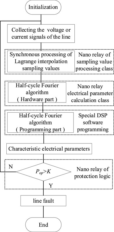
FIGURE 3. Calculation process of line selection protection for a small current grounding system based on hardware and software collaboration.
The general data processing flow of software–hardware collaboration chip-based relay protection is as follows:
(1) The SV data are entered into the FPGA—the SV subscription is parsed according to the configuration—and the sampled data needed to protect the CPU are written into the memory.
(2) The switch state entered the FPGA in the form of GOOSE messages—screened the GOOSE messages according to the configuration—wrote into the specific memory for GOOSE parsing—and transmitted the parsed switch information to the protection CPU through variables.
(3) The protection CPU calculates the power frequency and harmonic vector, compares the start and action conditions, and outputs the switch action command; a GOOSE task obtains the opening information through the variable and converts it into GOOSE message and sends it to the intelligent operation box through the FPGA.
Compared to the standard plug-in architecture, the “chip-based” device realizes the protection functions of the sample value and switch amount, and other information are exchanged in the chip through the memory. For the protection CPU, the key data are provided in the form of specific memory address mapping, without considering the synchronous scheduling of data processing process, so the corresponding time cost is also significantly reduced. The time granularity of communication task scheduling can be at the level of 100 us. Compared with the time required to identify physical quantities through Fourier computation and other methods, the information transmission cost can almost be ignored. The specific basis for reducing delay measurement is as follows:
(1) Data transfer from the SV interface to the protected CPU: Writing the data information subscribed by SV into memory in the SoC will reduce about 1 ms compared to sending the SV interface board of standard plug-in architecture to the CPU board.
(2) Switching quantity input, the SoC will directly share the memory to the protection CPU after the on-chip GOOSE is parsed, which will reduce by 1–2 ms compared with the GOOSE interface board with standard plug-in architecture and transmit the GOOSE to the CPU board through the internal network after the Goose is parsed.
(3) On/off output, the protection CPU will directly share the start and trip commands to the GOOSE module through the memory. Compared with the CPU board with standard box architecture, the start and trip commands will be transmitted to the GOOSE interface board through the internal network, and the packet output can be reduced by 1–2 ms.
(4) The protection of CPU fault processing tasks and SV and GOOSE processing tasks can be reduced by 0.5–2 ms under the condition of sharing an internal synchronization service.
It can be seen that on the basis of simplifying data synchronization between tasks, the chip-based protection device system can significantly reduce the protection action time that shorten about 5 ms on average. Also, the hardware architecture is simpler, and the system reliability is improved theoretically.
According to 《The dynamic test of the power system protective products》 (GB/T26864-011), to establish a real-time digital model of a system, the characteristics are highly consistent when compared in details with the physical simulation system and can be calibrated against each other, including a variety of voltage levels of lines, transformers, busbars, and reactors. At the same time, it meets the transformer protection, transmission line protection, busbar protection, circuit breaker protection, short lead protection, overvoltage and fault start device, and other relay protection, as well as fast switching device and automatic switching device debugging.
The dynamic mode test model is shown in Figure 4 and parameters are as shown in Tables 1–4.
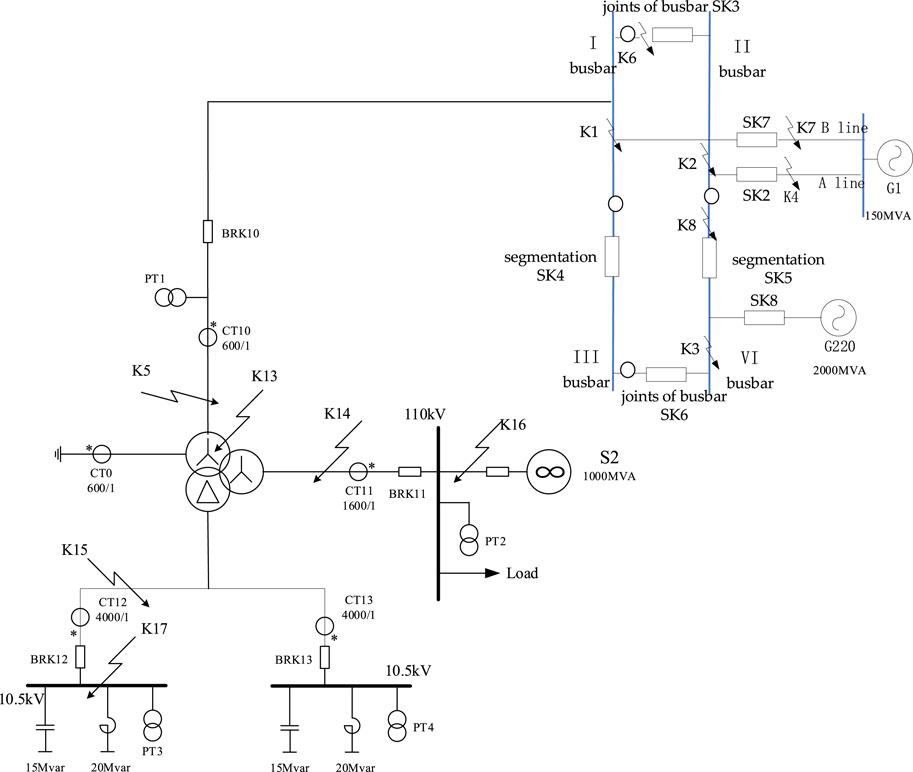
FIGURE 4. Double-bus double-section test system.

TABLE 1. Equivalent system parameters.
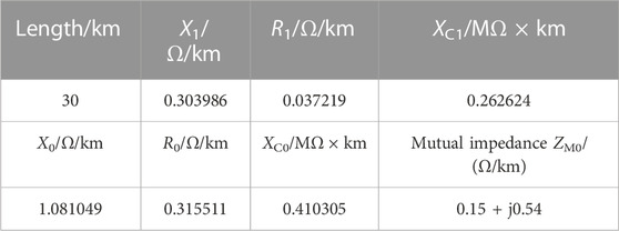
TABLE 2. Line parameters (220 kV double circuit transmission line parameters).

TABLE 3. Transformer parameters.
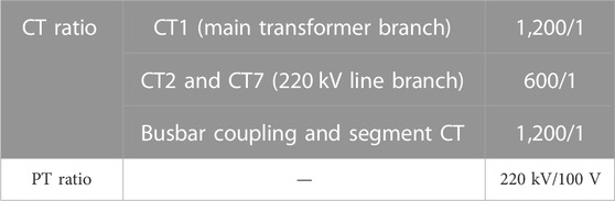
TABLE 4. CT and PT parameters.
The primary system of real-time digital simulation is connected with the chip protection device and a traditional microcomputer protection device through the power amplifier. The input and output are directly connected with the protection. The background host is connected with the primary system and protection device through the switch, and it realizes the control of the primary system model and collects the tripping signal and message information of the protection. The flowchart of the test method is shown in Figure 5. The test items include internal metallic fault, external metallic fault, system frequency deviation, and system oscillation.
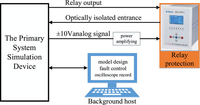
FIGURE 5. Flow chart of the test method.
After the experimental test and comparison, the comparison results between the technical parameters of the chip-based protection device and the microcomputer protection device were obtained, as shown in Table 5.
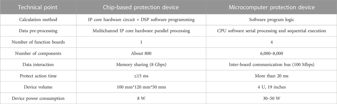
TABLE 5. Technical comparison between the chip-based protection device and microcomputer protection device.
In this paper, we install the chip protection devices in the substation to test and verify the function of the chip protection device. The experimental result of field operation is shown in Figure 6.
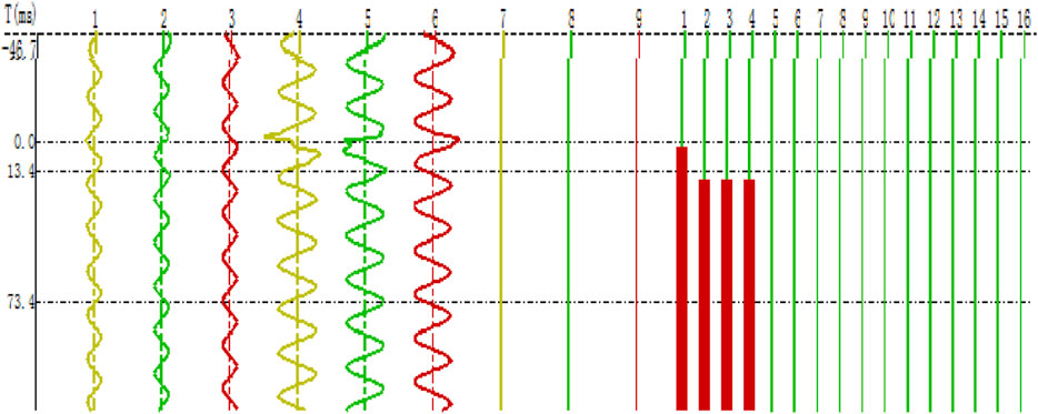
FIGURE 6. Third diagram of the chip protection device action.
Figure 6 shows that the device starts at 0 s; at the same time, it starts protect triggering, and it has collected the current of the bus and lines, and the chip protection device runs normally without failure.
The meaning of the abscissa in Figure 6 is shown in Table 6.
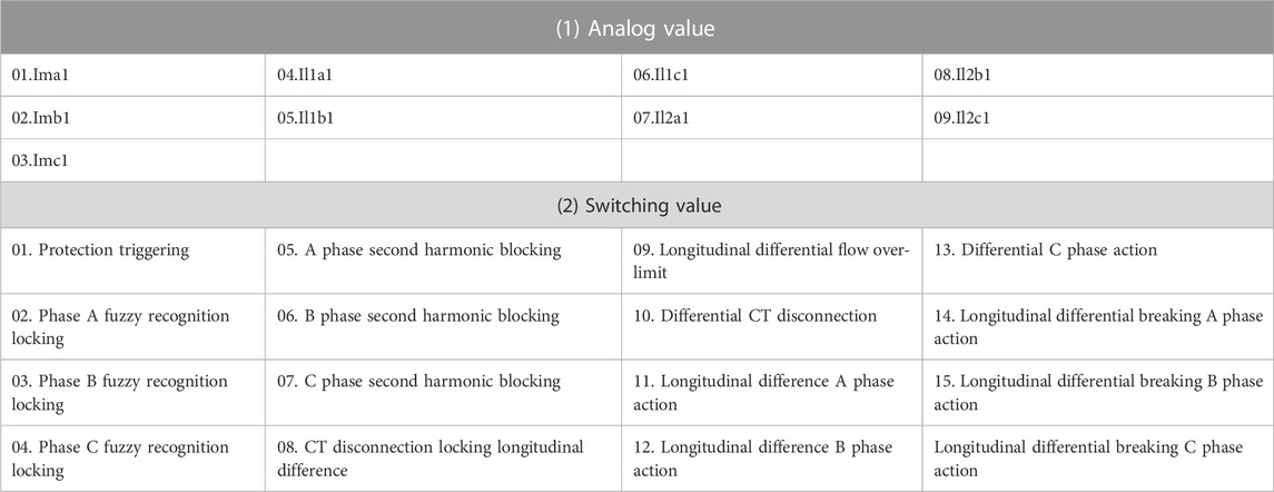
TABLE 6. Meaning of the abscissa in Figure 6.
In the figure, the top nine is the analog value and the last 16 columns are the switching value.
This section takes Guangdong Foshan 110 kV Ruiyan station as an example to explain the pilot application of a chip protection device interval in detail. 110 kV Ruiyan station is an indoor GIS substation, including two 63 MV. The main transformers, a 110-kV line transformer group connection mode, the main transformer high-voltage side, and the incoming line share the circuit breaker, #1 main transformer low-voltage-side single branch, and #2 main transformer low-voltage-side double branch. The main transformer of Ruiyan station and 110 kV incoming line secondary equipment included four 110 kV main transformer protections, four 110 kV main transformer merging units, and four 110 kV main transformer intelligent terminals. One chip-based protection device and one chip-based transformer protection device are in pilot.
The overall principles of the pilot operation of the chip-based protection device in the Ruiyan station and the Pailing station included independent network, only collect and not export, do not affect the original normal operation equipment, and realize the complete collection of the status information of the pilot equipment and operation status analysis of the device.
The 110-kV chip-based line protection device selects a 110-kV Ruiyan transformer, #2 main transformer incoming line, and 220 kV Pailing transformer with 110 kV line interval as the pilot application object.
Taking the 110 kV Ruiyan station as an example, #2 main transformer into line transformer group connection, high-voltage side, and line share the circuit breaker, electric CT, and PT. The chip line protection device is connected to the transformer’s high-voltage-side CT and the line PT. The CT takes the positive end away from the transformer side, and the direction of the distance element and the direction element is based on this. The original merging unit and intelligent terminal of the system are connected to the new switch in the pilot application. The chip line protection device is directly connected to the switch to collect the incoming line current, voltage, and switch position. The GOOSE tripping pressure plate of the chip line protection device is withdrawn to ensure that the chip protection does not act on the high-voltage side switch of the transformer after the action of the chip protection, so as to ensure that the trial operation of the chip protection does not affect the normal operation of the original system. The pilot scheme of the chip line protection device is shown in Figure 7A.
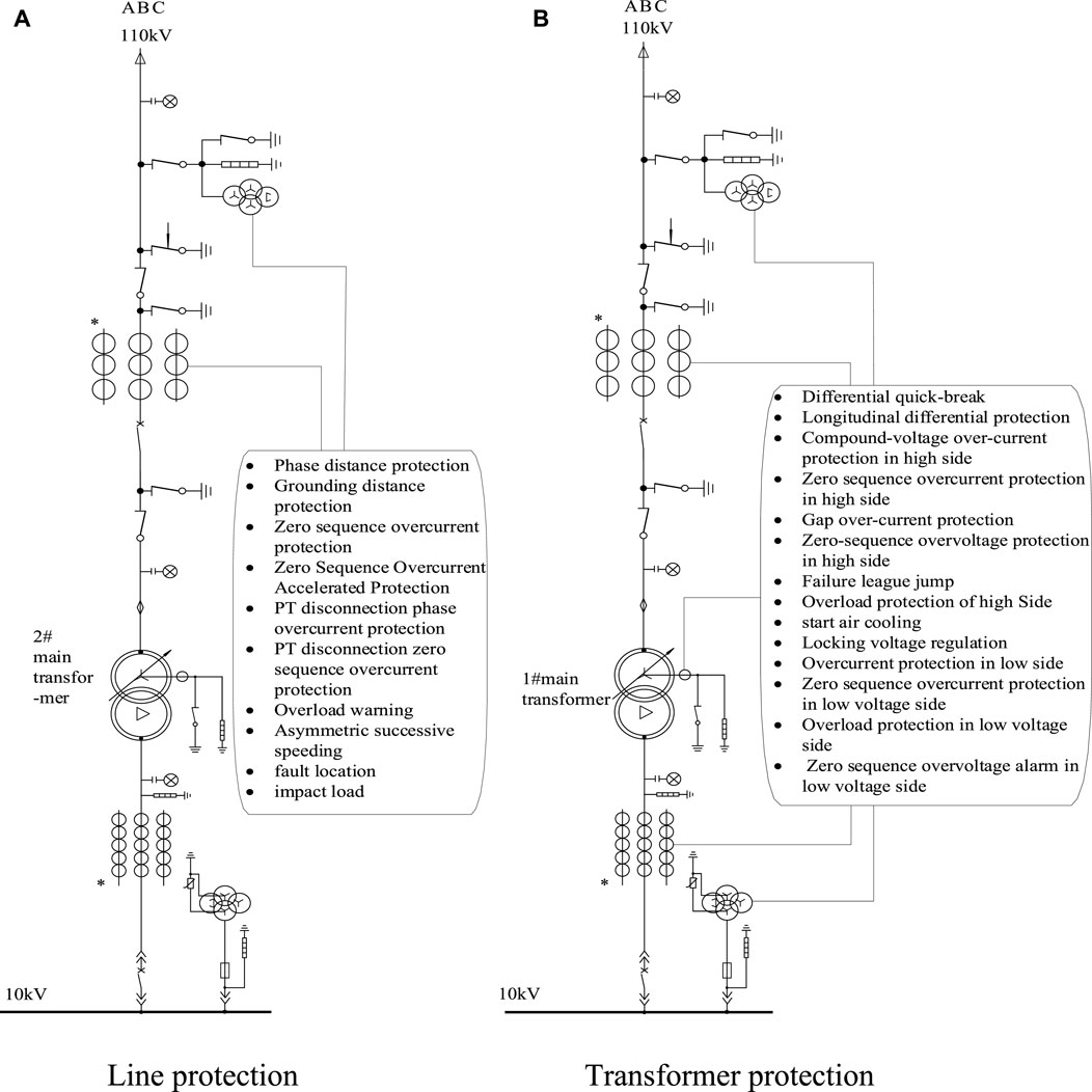
FIGURE 7. Pilot scheme for chip-based protection devices. (A) Line protection. (B) Transformer protection.
The 110-kV chip transformer protection device selects the #1 main transformer of the 110 kV Ruiyan station as the pilot application object, #1 main transformer is the line transformer group wiring mode, high-voltage side and line share circuit breaker, and low voltage side without branches. The CT of each side of the transformer is far away from the transformer side as the positive end, and the calculation of the differential current and the direction of the directional element are based on this. The original merging unit and intelligent terminal of the system are connected to the new switch in this pilot application, and the chip transformer protection is directly connected to this switch to collect the current, voltage, and switching position of each side of the transformer. The GOOSE tripping pressure plate of the chip transformer protection device is exited to ensure that the chip-based protection devices does not act on the switches on each side of the transformer after the action of the chip protection, so as to ensure that the trial operation of the chip protection does not affect the normal operation of the original system. The pilot scheme of the chip transformer protection device is shown in Figure 7B.
The 110 kV chipped transformer protection device of 110 kV Ruiyan substation is installed in the #1 line transformer group, and the 110 kV chipped line protection device is installed in the #2 line transformer group. The acquisition of current, voltage, and switch position of #1–2 line transformer groups is completed, and the corresponding protection function is put into operation, according to the fixed value of line and transformer protection. In order to ensure that the normal operation of the primary equipment is not affected, the outlet pressure plate of each protection is withdrawn. After the protection action, the corresponding information is sent to the monitoring background, and the tripping outlet does not act on the circuit breaker.
In order to minimize the impact on the original equipment, the substation is configured with an independent monitoring host, and the monitoring data are uploaded to the dispatching master station at all levels through the intelligent remote unified channel.
The secondary equipment monitoring data of 110 kV Ruiyan substation are modeled by the series standard of 《DL/T 860 Communication network and system in substations》 and 《technical specification of DL/T 1146 DL/T 860 in engineering》 to meet the standard conformance test. Station is divided into station control layer, interval layer, and process layer, according to the principle of three layers to network alone.
In the station, a time synchronization device and switch supporting 1588 function are added to form a separate SV, GOOSE, MMS, and 1588 synchronous four-in-one switch and network for the pilot use of the chip-based protection devices. The new clock device is connected to the original timing device IRIG-B code optical fiber interface in the station to output 1588 clocks and access the four-in-one switch; the GOOSE optical port and the merging unit SV optical port of the correlation interval intelligent terminal in the station are connected to the four-in-one switch; the station MMS network accesses the four-in-one switch through the Ethernet port; the four-in-one switch according to the needs of the network port shielding 1588 features to reduce the impact on existing equipment within the station; the aforementioned connections form a four-in-one network of SV, GOOSE, MMS, and 1588 synchronization, which is connected to the chip transformer protection device and the chip line protection device.
The system network structure diagram is shown in Figure 8.
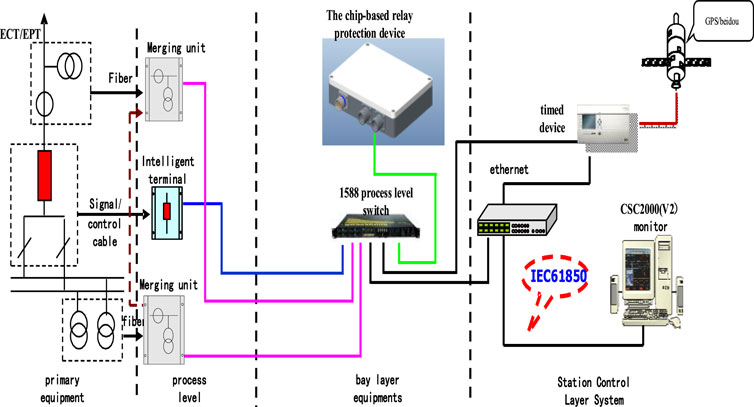
FIGURE 8. Diagram of the system network structure.
In order to highlight the advantages of high protection level, high anti-interference, miniaturization, and suitable for on-site installation, the 110-kV chip transformer protection device is installed on the roof of Ruiyan station, directly exposed to high temperature exposure environment. The 110 kV chip line protection is installed in the 110 kV voltage level GIS equipment area of Ruiyan station and Pailing station, receiving high intensity electromagnetic radiation.
A corresponding size base is added to the substation roof and GIS equipment area to fix the local chip protection device. In order to ensure the power supply of the chip protection device and the communication connection with the secondary equipment of the main control room, the connection cable related to the chip line protection is laid in the same trench with other secondary cables in the 110 kV equipment area, and the connection cable related to the chip transformer protection is buried to the roof through the wall body. Figure 9 shows the site photo of the chip-based protection device.
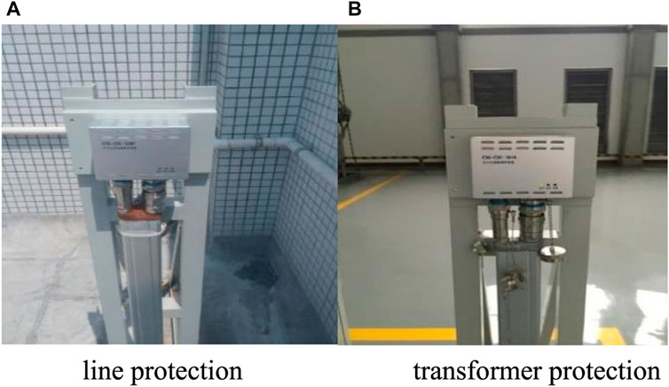
FIGURE 9. On-site installation of the 110 kV chip protection device applied in line and transformer protection.
Since the commissioning of the chip protection device, it has experienced extreme weather such as high temperature, wind, rain, cold wave, and so on. It runs in the complex electromagnetic environment, such as transformer and GIS switch line, and shows good stability performance. There is no misoperation, rejection, and false alarm, which ensure the safe and stable operation of the substation.
During the trial operation, there are no occurring grid faults in each substation. Meanwhile, the chip transformer, line protection, and conventional corresponding protection did not act, and the action behavior was consistent. The protection start-up event is triggered when the power grid is disturbed. The statistics of chip protection SOE information and protection action report information show that the start-up times of transformer protection and line protection in Foshan Ruiyan station are more than 500 times, the start-up times of transformer protection in Guiyang Beimen station are more than 500 times, and the start-up times of line protection in Guiyang Sunlin station are 14 times (abnormal SV data sampling after March 2017 lead to unqualified trigger protection start-up events). The statistical results are shown in Table 7.
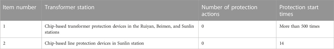
TABLE 7. Statistics of chip protection action/start times.
Taking a certain month of Beimen substation as an example, the typical start-up conditions of chip protection and conventional protection are counted. The comparison is shown in Table 8. The comparison shows that when the power grid is disturbed, the chip protection and the conventional protection start at the same time, and the protection start-up behavior is consistent.
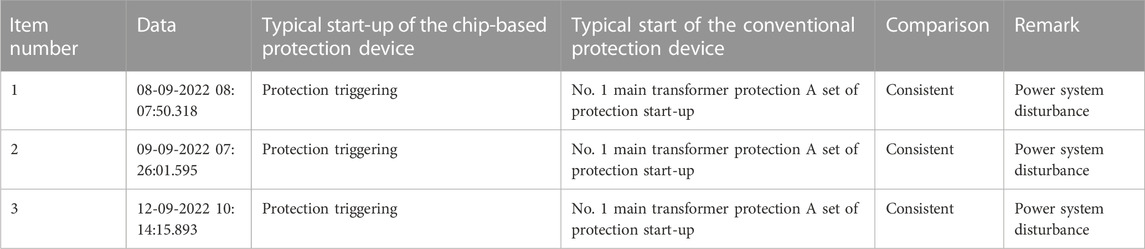
TABLE 8. Comparison statistics of typical start-up of chip-based protection devices and conventional protection devices in Northgate station.
On 08 September 2022 08:07:50, the grid current of Beimen substation is distorted, resulting in zero sequence, which leads to zero sequence overcurrent start chip and conventional protection recording. The process is shown in Figure 10.
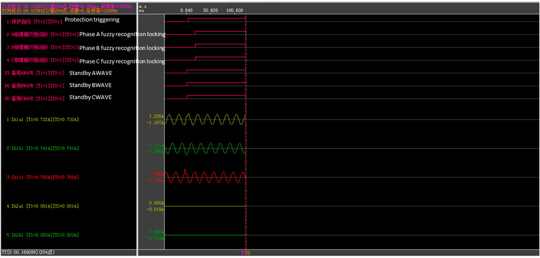
FIGURE 10. Protection start waveform diagram of chip-based transformer protection devices in Beimen substation.
Figure 10 shows that when a fault occurs, the protection starts at 0.648 ms, the A, B, and C three-phase fuzzy identification blocking starts at the same time, and the standby ABC starts immediately when the protection is triggered. The three-phase current of A, B, and C are distorted within a few milliseconds of the protection touch time, but the protection immediately returns to normal after the protection is started.
At the same time, taking Ruiyan station as an example, the protection correctly triggered the start-up event and recorded the disturbance wave when the power grid was disturbed. At 8:47 on 22 June 2018, the grid current of Ruiyan station was obviously disturbed, and the chip line protection started the waveform correctly, as shown in Figure 11.
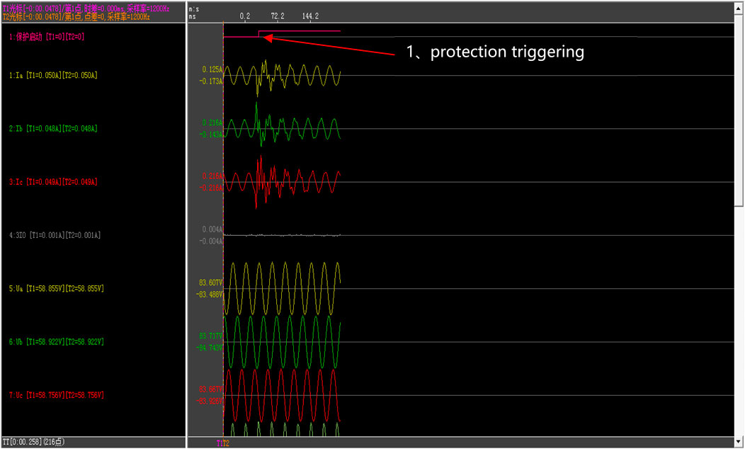
FIGURE 11. Start waveform diagram of chip line protection in Ruiyan station.
Figure 11 shows when the power grid is disturbed, the three-phase current of A, B, and C is distorted. After the protection is triggered, the normal value is restored immediately.
In this paper, the system-on-chip-based relay protection technology is proposed. The architecture design of SoC, hardware and software cooperative relay protection based on the system-on-chip IP core and engineering application are expounded. Through hardware algorithm engine acceleration and hardware and software cooperative calculation, the performance of high-speed data acquisition and interaction is significantly improved.
(1) The message processing efficiency is improved as the chip protection device makes full use of the high parallel processing efficiency of the power dedicated algorithm hardware unit, and changes the SV parsing, filtering, interpolation, and other tasks originally implemented by the CPU to be implemented by the on-chip power-dedicated algorithm hardware unit.
(2) The overall performance of the protection device is improved, as the function of the device is realized by a single chip with high integration, which reduces the interaction link and shortens the protection action time. At the same time, the action time of the fast section is 5 ms shorter than that of the conventional digital protection device.
(3) The relay protection SoC proposed in this paper is helpful to realize the local equipment operation and the fusion of primary and secondary equipment and improve the reliability and stability of a relay protection device.
The original contributions presented in the study are included in the article/supplementary materials; further inquiries can be directed to the corresponding author.
XL conceptualized the overall structure and framework of the article, as well as conceptualized the outline of the manuscript and experiment validation. WX helped write the manuscript with constructive discussions. YY and HY wrote the manuscript and generated the figures and performed experiment validation. All authors contributed to the article and approved the submitted version.
This work was supported by the Technology Project of China Southern Power Grid (ZBKJXM20180500). The funder was not involved in the study design, collection, analysis, interpretation of data, the writing of this article, or the decision to submit it for publication.
Authors XL, WX, YY, and HY were employed by the company China Southern Power Grid.
All claims expressed in this article are solely those of the authors and do not necessarily represent those of their affiliated organizations, or those of the publisher, the editors, and the reviewers. Any product that may be evaluated in this article, or claim that may be made by its manufacturer, is not guaranteed or endorsed by the publisher.
Cao, B., and Huang, H. S. (2014). Design and implement of a system-on-chip. Electron. Des. Eng. 22 (9), 16–19. in Chinese. doi:10.14022/j.cnki.dzsjgc.2014.09.029
Chen, G. P., Wang, D. L., and Qiu, Y. T., (2017). Challenges and development prospects of relay protection technology. Automation Electr. Power Syst. 41 (16), 1–11+26. in Chinese. doi:10.7500/AEPS20170219004
Chen, K. M., Liu, P., and Wang, W. D., (2007).Scheme to optimize real-time bus scheduling in multiprocessor SoC for media processing. J. Zhejiang Univ. Eng. Sci. 2007 (9),1546–1551. in Chinese. doi:10.7500/AEPS20170219004
Graham, B., Rich, H., and Jeff, W. (2013). Low cost implementation of high performance PCle Gen2 hard core. Ip. China Integr. Circ. 22 (9), 41–44. in Chinese. doi:10.3969/j.issn.1681-5289.2013.09.006
Li, P. F., Tang, Z. A., Wang, K. Y., Chao, M., and Qu, H., (2009). FPGA-Based dynamic self-reconfiguration embedded system design. China Intergrated Circ. 18 (6), 5. in Chinese. doi:10.3969/j.issn.1681-5289.2009.06.010
Liu, L. J., and Yu, L. (2014). Review of present situation and development of relay protection in power system. Sci. Technol. Vis. 26, 49. in Chinese. doi:10.19694/j.cnki.issn2095-2457.2014.26.216
Lv, H., Zhang, S. B., Wang, J., Liu, S., and Jing, D. S., (2021). Implementation of convolutional neural network SIP microsystem. Comput. Eng. Appl. 57 (5), 6. in Chinese. doi:10.3778/j.issn.1002-8331.2009-0011
Wu, H. M., Shi, Q., and Chen, C. Z. (2019). IP technology of IC design and IP characteristics in IC industrial development. Micro/nano Electron. Intelligent Manuf. 1 (1), 20–28. in Chinese. doi:10.19816/j.cnki.10-1594/tn.2019.01.003
Xi, W., Yao, H., Cai, T. T., Chen, B., Chen, H. M., Wang, Y. Q., et al. (2016). Research on chip-based protection and measuring and control devices. Power Syst. Clean Energy 32 (11), 91–97. in Chinese. doi:10.3969/j.issn.1674-3814.2016.11.016
Xi, W., Yao, H., Chen, B., Chen, H. M., Wang, T. J., Chen, Q. R., et al. (2017). Design of protection device based on SOC system data exchange. J. Electr. Power Sci. Technol. 32 (3), 121–125. in Chinese. doi:10.3969/j.issn.1673-9140.2017.03.019
Yang, B., Chu, Y. Q., Jing, D. S., and Gao, H., (2020). Design and verification of IP core for controlling discrete signals in so C based on AXI4 bus. Information&Communications 3, 90–92. in Chinese. doi:10.3969/j.issn.1673-1131.2020.03.036
Ye, Q. (2021). China Southern Power Grid Digital Grid Research Institute Co., Ltd.: Achieving the large-scale application in developing first power dedicated master chip that is named "Fuxi" in China. Guangdong Sci. Technol. 30 (9), 29–30. in Chinese.
Keywords: system-on-chip, relay protection, hardware and software collaboration, primary and secondary equipment integration, power grid
Citation: Li X, Xi W, Yu Y and Yao H (2023) Research of the system-on-chip-based relay protection technology. Front. Energy Res. 11:1105148. doi: 10.3389/fenrg.2023.1105148
Received: 22 November 2022; Accepted: 27 February 2023;
Published: 25 October 2023.
Edited by:
Dongqi Liu, Changsha University of Science and Technology, ChinaReviewed by:
Hang Zhong, Hunan University, ChinaCopyright © 2023 Li, Xi, Yu and Yao. This is an open-access article distributed under the terms of the Creative Commons Attribution License (CC BY). The use, distribution or reproduction in other forums is permitted, provided the original author(s) and the copyright owner(s) are credited and that the original publication in this journal is cited, in accordance with accepted academic practice. No use, distribution or reproduction is permitted which does not comply with these terms.
*Correspondence: Xiaobo Li, bGl4YjFAY3NnLmNu
Disclaimer: All claims expressed in this article are solely those of the authors and do not necessarily represent those of their affiliated organizations, or those of the publisher, the editors and the reviewers. Any product that may be evaluated in this article or claim that may be made by its manufacturer is not guaranteed or endorsed by the publisher.
Research integrity at Frontiers
Learn more about the work of our research integrity team to safeguard the quality of each article we publish.