 Shaowen Cao1
 Qilin Cai
 Qing Ye
- 1College of Energy, Soochow Institute for Energy and Materials Innovations, Soochow University, Suzhou, China
- 2Sunleem Technology Incorporated Company, Suzhou, China
In this paper, a thermophotovoltaic (TPV) emitter that combines a one-dimensional photonic crystal with two-dimensional periodic nanoarray cavities was proposed. The Finite-Difference Time-Domain (FDTD) method was adopted to analyze the spectral emittance and its sensitivity to the emission angle for the proposed emitter. The results show that the main emission mechanisms of the emitter are Cavity Resonances (CRs), Fabry-Perot (FP) resonances, and Magnetic polaritons (MPs). In the convertible band of a TPV cell, CRs and FP resonances are coupled together to broaden the emitting bandwidth of the emitter. The cut-off wavelength of structural spectral emittance increases with depth and radius but decreases with a period. In addition, the spectral emittance is non-sensitive to the emission angle of less than 50°, highlighting the wide-angle stability of the composite structure. The proposed emitter has wide-angle adaptability and achieves a fine-tunning of bandgap wavelength while maintaining a good spectral selectivity. This work provides new insight into the design of the TPV emitter.
1 Introduction
Thermophotovoltaic (TPV) systems are cutting-edge thermoelectric conversion technologies that can utilize a variety of energy sources such as chemical energy (Nguyen-Huu et al., 2016), biomass energy (Silva-Oelker et al., 2018), nuclear energy (Zhu et al., 2013), and solar energy (Song et al., 2022) for silent power generation (Burger et al., 2020), and they have promising applications in aerospace (Song et al., 2015), distributed cogeneration (Fraas et al., 2003; Bianchi et al., 2012), solar energy conversion (Cai et al., 2020), and waste heat utilization (Celanovic et al., 2008). The TPV system contains two core components, i.e., emitter and TPV cell. The former mainly absorbs heat energy, which can be converted into radiative energy incident into the TPV cell; the latter converts the radiative energy into electricity. Notice that only photons with energy higher than the bandgap of the cell can generate electron-hole pairs. To improve the efficiency of the TPV system, it is crucial to modulate the emission spectrum of the emitter, i.e., the emittance is close to 1 in the convertible band and reaches 0 in the non-convertible band.
To achieve spectral tuning of emitters, the researchers designed micro-nano structures on materials to generate Surface Plasmon Polaritons (SPPs), Magnetic Polaritons (MPs), Fabry-Pérot (FP) interference effects, and Cavity Resonances (CRs) to achieve selective emission of emitters based on the micro-nano scale heat transfer theory. Typical micro- and nano-structures include one-dimensional layered stacks (Silva-Oelker et al., 2019), one-dimensional grating structures (Song et al., 2015; Silva-Oelker et al., 2018), two-dimensional cavity array structures (Chou et al., 2014; Ye et al., 2015), two-dimensional grating structures (Zhao et al., 2013; Song et al., 2016), metamaterials (Molesky et al., 2013; Dyachenko et al., 2016) and three-dimensional photonic crystal structures (Farfan et al., 2010). Compared with two- and three-dimensional structures, one-dimensional layered stacked emitters have received widespread attention because of their relative convenience of fabrication. Blandre et al. (2018) investigated the Mo-HfO2 three-layer stack structure and found that the spectral selectivity of this structure is mainly caused by the FP resonance effect. However, this effect is dependent on the material thickness when the material is fixed, resulting in limited spectral tuning capability. Therefore, although the two-dimensional structured emitters are relatively complex, they also show attractive development potential due to their scalable fabrication (Yeng et al., 2012) and convenient spectral tuning (Celanovic et al., 2008). Ye et al. (2015) adopted the FDTD method to study the two-dimensional photonic crystal based on VO2 materials, and found that there exhibits the CRs effect in the short wavelength band, resulting in spectral selectivity. CRs are dependent on these parameters, i.e., cavity radius, period, and depth. Compared with the FP resonance effect of one-dimensional structures, CRs can enhance the spectral control ability of the emitter. In addition, Rostamnejadi et al. also investigated the effects of structural parameters and temperature on cylindrical 2D W photonic crystals with the FDTD method (Rostamnejadi and Daneshvar, 2018), indicating that the emittance at 1500 K is higher than that of 300 K. The main reason is that the electron-phonon interaction enhances with increasing temperature. Therefore, to match different operating temperatures of the TPV system, the period, depth, and radius of the 2D array cavity can also be optimized. It should be noted that although the two-dimensional microcavity structure can be spectrally tuned through multiple dimensions, its spectral emittance is significantly influenced by the incident angle and polarization mode. According to the literature (Yeng et al., 2012), the spectral selectivity of the two-dimensional microcavity structure disappears at incidence angles greater than 30°, the spectral emittance of the cell’s operating band decreases, and that of the non-convertible band increases. For a practical TPV emitter, the incident wave is not always the normal TM wave, requiring that the emitter should be spectrally selective for incident waves with different polarization modes and different incidence angles (Khodasevych et al., 2015; Kim et al., 2017; Sakakibara et al., 2019). Comparing with normal incidence, the spectral selectivity of the emitter decreases under oblique incidence, leading to a decrease in the overall efficiency of the TPV system (Ulaby et al., 2015; Jiang et al., 2019). Therefore, it is crucial to maintain the adaptability of the emitter’s wide-angle and polarization method.
The researchers investigated the adaptability performance of the emitter’s wide-angle and polarization mode. For example, Silva-Oelker et al. (2019) showed that the spectral emittance of 1D stacked structures varies less with the polarization mode and the incident angle. Due to the fact that the emission mechanism of 1D layered structures is mainly the FP resonance and this resonance emission is almost independent of the incident angle and the polarization mode. Wang et al. also investigated the effect of incident angle on SPPs and MPs based on a one-dimensional grating-type emitter (Wang and Zhang, 2012), and found that SPPs are most sensitive to the incident angles, while MPs remain constant. Thus, the emitters relying on resonant emission from SPPs are less adaptable to the angle. Chou et al. (2014) analyzed the effect of incident angle on the CRs based on a two-dimensional cavity emitter and found that the resonant emittance decays rapidly with increasing incident angle. This is mainly because the incident light cannot be coupled efficiently into the cavity mode as the incidence angle increases, the diffraction loss causes the radiation to reflect into unwanted diffraction channels instead of coupling into the cavity mode. In addition, regarding to the adaptation of the polarization mode, the spectral emittances of TM-polarized and TE-polarized waves are equal when the symmetric structure is normal to the incident direction. However, when the incident wave is oblique, the symmetry of the structure can be broken, resulting in the spectral emittance of the TM polarization no longer being equal to that of the TE polarization (Zhao et al., 2013). In the work of Khodasevych et al. (2015), it was reported that TM polarization is usually more adaptive to oblique incidence angles than TE polarized waves, maintaining higher absorption levels in the structure at incidence angles up to 10° or greater.
To sum up, it is found that the spectral modulation for the one-dimensional emitters with layered structures mainly depends on the FP resonance effect. Also, it has good adaptability to the incident wave polarization mode and the incident angle. However, the ability of spectral modulation based on layer thickness is limited. The two-dimensional structure can adjust the spectral tuning characteristics by changing the radius, period, and depth of the array cavity to match different operating temperatures or TPV cells, whose spectral emittance is limited by the angle of incidence and polarization mode. Consequently, the existing emitters fail to achieve a combination of excellent spectral tuning capability and wide-angle adaptability. On this basis, the research idea of combining one-dimensional and two-dimensional structures was proposed to realize the combination of the advantages of both. To confirm the feasibility, it is necessary to explore the mechanism of the spectral modulation of the proposed emitter.
In this work, a structure based on laminar stacked composite periodic nanoarray cavities was proposed, which aims to improve the wide-angle adaptability of the two-dimensional array cavity structure while enhancing the spectral modulation capability. Firstly, Maxwell’s equation system was solved based on the FDTD algorithm to obtain the electromagnetic field distribution in the simulation area. Secondly, the mechanism of resonant emission from the structure was analyzed based on the coupled-mode theory, FP interference theory, and MPs capacitance-inductance equivalent circuit model. Then, the spectral emittance of the emitter was adjusted to better match the InGaAsSb cell by optimizing the structure radius, period, number of layer pairs, etc. Finally, to evaluate the optical performance of the emitter, the directional spectral emittance of the TPV emitter was calculated and analyzed.
2 Model design and numerical simulation methods
2.1 Model design
Figure 1 shows a schematic diagram of the two-dimensional layered periodic array cavity structure, which mainly consists of a one-dimensional laminar photonic crystal and a two-dimensional cylindrical cavity array. The structural substrate is a metal layer (∼5 μm), which is thick enough to suppress the infrared radiation transmission. The dielectric and metal layers are alternately stacked on the substrate, and their thicknesses are denoted as dD and dM, respectively. For convenience, a single metal layer and a dielectric layer are referred to as a layer-pair (LP). The cavity array has the same period of a in both x and y directions. The cavity depth, radius, and refractive index are set as h, r, and nc, respectively. In addition, to obtain the spectral emittance of the structure, the wave vector (kinc) is introduced, which represents a planar electromagnetic wave at the wavelength of λ incident on the structure at the incident angle (θ), azimuth angle (φ) and polarization angle (ψ). Here, ψ = 0° and ψ = 90° represent TM and TE waves, respectively. It is known from the literature (Zhang, 2007) that the spectral emittance of the symmetric surface is independent of the azimuthal angle. Thus, the azimuthal angle (φ) is set to 0° in this work to simplify the calculation.
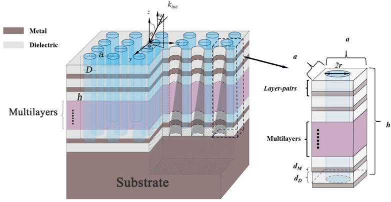
FIGURE 1. Schematic diagram of the layered stack structure of the composite nanoarray cavity, the black dashed line in the figure indicates a periodic cell.
Because the operating temperature of the emitter is usually in the range of 1,000–2000 K, it is necessary to choose the refractory materials for the emitter design. Mo exhibits an inherent spectral selectivity with in-band absorption and has a high melting point, making it a good candidate for the metal layer of the TPV emitter. In addition, HfO2 also has a high melting point and has a similar coefficient of thermal expansion (5.97 × 10⁻⁶ K−1) to that (5.45 × 10⁻⁶ K−1) of Mo at 1500 K, respectively (Zhang et al., 2022). Thus, Mo and HfO2 were selected as the metal and dielectric layer materials, respectively. Their optical constants can be obtained from the literature (Palik, 1998).
2.2 Numerical simulation method–FDTD theoretical calculation
In this work, the thermal radiation properties of the structure are calculated by solving the system of Maxwell’s equations using the FDTD algorithm. The method has been widely used in the calculation of the electromagnetic field of the radiator, which generates Maxwell’s spinor equations as a discrete matrix equation of the electromagnetic field, and the differential form of Maxwell’s equations can be expressed as (Yang et al., 2017):
where E, H, D, B, J, and ρ are the electric field strength vector, magnetic field strength vector, potential shift vector, magnetic induction strength vector, current density vector, and charge density, respectively. There is an intrinsic structure relationship between the above values:
where ε and μ are the dielectric constant and magnetic permeability, respectively.
In this work, the Periodic Boundary Condition (PBC) is adopted in the x and y directions for normal incidence. However, the Bloch boundary condition is applied for the oblique incidence, which is a general case of PBC and more applicable to the case of the oblique incidence. Using the above boundary conditions, a cell can be analyzed. Because the x and y directions have the same structure, the PBC can be transformed into a time-domain form by considering the periodic structure in the one-dimensional case in the x and z directions:
where P is a component of the electromagnetic field component in the frequency domain, a is the period length, νϕc = c/sinθ is the phase velocity (in the x direction), c is the speed of light, and θ is the angle of incidence. Using the Perfectly Matched Layer (PML) boundary condition in the z-direction to keep no reflections on the boundary, the wave impedance of the PML cutoff can be written as:
The final matching condition is obtained as:
where σm is the magnetic permeability in the PML medium, σ is the electrical conductivity, and μ0 and ε0 are the magnetic permeability and dielectric constant of the vacuum, respectively. On the basis of the control equations and boundary conditions, the equations are discretized according to the Yee algorithm. The FDTD method can be adopted to solve the electromagnetic field of the whole space step by step when the initial values and boundary conditions of the electromagnetic field problem are given.
The incident light in this work is a plane wave of Bloch/periodic type, with the direction of incidence downward along the z-direction. To optimize the calculation time and to ensure accuracy, at least 10 cells per wavelength and appropriate time steps are needed. The grid size can be determined by the lower limit of the studied spectral range (dmesh ≤ λ/10n, where n is the refractive index of each layer in the cell) (Mandal, 2021). The reflectance [R (λ, T, θ, ψ)] and transmittance [τ (λ, T, θ, ψ)] of the directional spectrum of the structure are calculated. Furthermore, according to the radiative properties of the opaque medium, τ (λ, T, θ, ψ) ≈ 0, the absorption of the directional spectrum of the structure can be calculated as:
Finally, according to Kirchhoff’s law, the absorbance of the structure directional spectrum is equal to the emittance:
2.3 Thermophotovoltaic emitter optical performance evaluation
The optical performance of the emitter is evaluated based on the spectral efficiency, which is the ratio of the amount of radiation (
In this study, the InGaAsSb cell with a radiative convertible band of 0.3–2.4 μm was adopted, and thus, λg = 2.4 μm. In addition, the emitter temperature is set to 1500 K. Notice that 97% of the blackbody radiation energy is concentrated in the wavelength range of 0.3–10 μm at this temperature, this wavelength range is adopted for calculation in this work. The directional spectral efficiency was calculated to evaluate the optical performance of a TPV emitter with a certain incidence:
where εR (λ, T, θ, ψ) is the directional spectral emittance as a function of λ, T, θ and ψ, and E λ, b (λ, T) is the blackbody spectral intensity at temperature T:
where hp is Planck’s constant, c0 is the speed of light, and k is Boltzmann’s constant.
3 Results and discussion
3.1 Selection of structural characteristics parameters
To investigate the effect on the spectral tuning performance after the composite nanocavity array of one-dimensional layered stack structure, the transient electromagnetic field variation and normal spectral emittance of the composite structure were calculated using FDTD numerical simulation. First, the layered structure parameters are selected, and according to the results of the literature (Blandre et al., 2018), the one-dimensional emitter matches better with the TPV cell when dM = 10 nm and dD = 80 nm. Therefore, the thicknesses of the Mo and HfO2 layer are set as 10 nm and 80 nm for initial calculation, respectively. Second, to choose the parameters of the array cavity structure, the waveband in which the cavity two-dimensional structure resonates can be predicted based on the coupled-mode theory (Ye et al., 2015; Song et al., 2016; Jiang et al., 2021)
where Bm, Bn, and Bp are integers, and for TM mode, Bp = 0, χBmBn denotes the Bn th root of the first class of Bm order Bessel functions, Bm = 0, Bn = 1, χ01 = 2.4048; while for TE mode, Bp = 1, χBmBn is replaced by χ'BmBn, which is the Bn th root of the first class of Bm-order Bessel functions derivatives, Bm = 1, Bn = 1, and χ'11 = 1.8412. r is the cavity radius, h is the cavity depth, μc and εc are the magnetic permeability and dielectric constant of the cavity medium, respectively, and c is the speed of light.
Based on Eq. 11, the cutoff wavelength of CRs can be predicted when the radius and depth of the array cavity are given. We took r = 600 nm, a = 2000 nm, and h = 900 nm based on the results of the literature (Ye et al., 2015), and the cutoff wavelength of CRs at this parameter is predicted to be approximately 2 μm. When h = 900 nm, the LP of the structure should be 10 [i.e., (80 + 10) × 10 = 900]. Thus, we calculated the spectral emittance for the geometric feature parameters LP = 10, dM = 10 nm, dD = 80 nm, r = 600 nm, a = 2000 nm, h = 900 nm, and nc = 1, as shown in Figure 2. It can be seen that the structure forms multiple resonant emission peaks in the wavelength range of 0.3–5 μm. Nonetheless, such spectral performance is not applicable to the design requirements of TPV emitters. As shown by the results of the literature (Mandal, 2021), for plasmonic multilayer hypersurfaces containing nano-cylindrical cavities, when multiple standing waves appear in the electromagnetic field inside the array cavity, multiband absorption is caused by the interaction of SPPs\CRs and MPs.
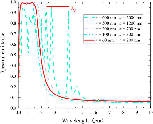
FIGURE 2. When other parameters are fixed (LP = 10, dM = 10 nm, dD = 80 nm, h = 900 nm (90*10), nc = 1), the comparison of spectral emittance for radius and period changes (r = 600 nm, a = 2000 nm, r = 500 nm, a = 1,200 nm, r = 300 nm, a = 700 nm, r = 100 nm, a = 300 nm and r = 60 nm, a = 200 nm).
On this basis, we consider reducing the array cavity radius until no multi-band absorption occurs in the 0.3–10 μm band. In addition, due to the results of the literature (Chou et al., 2014), for two-dimensional structured emitters obtaining better spectral performance, the period should ideally be only slightly larger than the diameter. Therefore, we reduced the radius from 600 nm to 60 nm, and its period is only slightly larger than the diameter until we found a more suitable geometry for the TPV emitter. Figure 2 shows the spectral emittance when the other parameters are consistent (LP = 10, dM = 10 nm, dD = 80 nm, h = 900 nm (90 × 10), nc = 1) and the radius r decreases gradually and the period is only slightly larger than the diameter (Chou et al., 2014) (r = 600 nm, a = 2000 nm, r = 500 nm, a = 1,200 nm, r = 300 nm, a = 700 nm, r = 100 nm, a = 300 nm and r = 60 nm, a = 200 nm). As can be seen, the spectral emission characteristics of the structure meet the design requirements of the TPV emitter when the radius is less than 300 nm. The composite structure array holes can be fabricated by nanoimprinting technology (Sakakibara et al., 2019), and the accuracy of current nanoimprinting technology can reach 15 nm. As a result, we choose r = 60 nm and a = 200 nm as typical structure parameters for the research.
3.2 Main emission mechanisms of the structure: The effect of cavity resonances, fabry-Pérot resonances, magnetic polaritons
To explore the effect of the Mo-HfO2 based multilayer stack structure after combining array cavity on the spectral modulation performance. We calculated and compared the normal spectral emittance of the one-dimensional structure, two-dimensional array cavity structure, and composite structure using FDTD, respectively. And the results are shown in Figure 3, where the geometrical characteristics of the one-dimensional structure are LP = 10, dM = 10 nm, dD = 80 nm; the two-dimensional structure uses Mo substrate and the structural parameters are r = 60 nm, a = 200 nm, h = 900 nm, nc = 1. Other than that, to verify the validity of the prediction of the coupled-mode theory for the two-dimensional cavity structure, the normal spectral emittance of the two-dimensional Mo photonic crystal with structural parameters of r = 600 nm, a = 2000 nm, h = 900 nm, and nc = 1, was also calculated. The structural parameters of the composite structure are the typical structural parameters selected above (LP = 10, dM = 10 nm, dD = 80 nm, h = 900 nm (90 × 10), nc = 1, r = 60 nm, a = 200 nm).
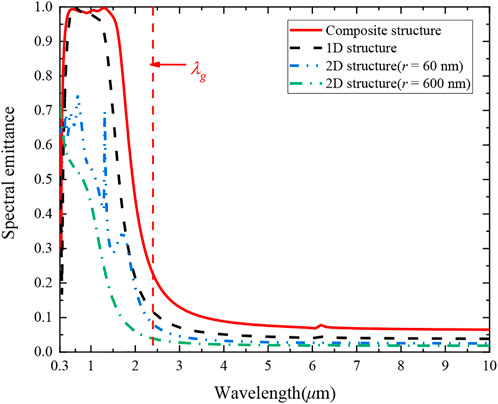
FIGURE 3. Comparison of spectral emittance of one-dimensional structures (LP = 10, dM = 10 nm, dD = 80 nm), two-dimensional array cavity structures (r = 60 nm, a = 200 nm, h = 900nm, nc = 1and r = 600 nm, a = 1,300 nm, h = 900nm, nc = 1) and composite structures (LP = 10, dM = 10 nm, dD = 80 nm, r = 60 nm, a = 200 nm, h = 900 nm, nc = 1).
It can be seen from Figure 3 that in the radiation convertible band (0.3–2.4 μm) of the InGaAsSb cell, the emission bandwidth can be broadened after the layered stack structure composite nanoarray cavity, and the spectral emittance in the range of 0.4–1.6 μm is greater than 0.95. The spectral high emission bandwidth is 42% wider than that of the one-dimensional structure. Widening the emission bandwidth of the TPV emitter can simultaneously increase the short-circuit current and open-circuit voltage of the TPV cell, which can improve the power output density of the system (Papadakis et al., 2020). In addition, the literature (Bani et al., 2018) investigated the variation of the forbidden bandwidth of the cell with temperature and found that the cutoff wavelength of the cell increases with temperature within 290–340 K, which also indicates the necessity of widening the emission bandwidth of the emitter. Observing Figure 3, it is found that the spectral emittance of the composite structure is also increased in the non-convertible waveband (2.4–10 μm) of the InGaAsSb cell, which is consistent with the previous report in the literature (Molesky et al., 2013; Dyachenko et al., 2016). It can be mainly attributed to the fact that the multilayer structure shows non-resonant emission in the long wavelength band. This is supported by the fact that the 2D structure does not have a multilayer structure, and therefore, it has a lower spectral emittance in the 2.4–10 μm range.
The spectral modulation performance of the stacked structure can be calculated and analyzed by the FP interference effect theory. Meanwhile, the non-composite cavity region of the proposed structure can be regarded as a one-dimensional structure. According to the results of the literature (Blandre et al., 2018), it is calculated that when the structural parameters of the layered structure are dM = 10 nm and dD = 80 nm, it produces two interference resonance peaks at λ = 0.5382 μm and λ = 1.1636 μm. Numerical simulations using FDTD reveal that the emission spectra can produce resonance peaks at λ = 0.5831 μm and λ = 1.1647 μm, and the numerical simulation results are in agreement with the theoretical results. This indicates that one of the reasons for the emission resonance of the composite structure is the FP interference effect.
In addition, the cutoff wavelengths of the corresponding emitting CRs are 0.1568 μm and 1.5661 μm for the two-dimensional cavity structure r = 60 nm and r = 600 nm as predicted by Eq. 11. It can be observed from Figure 3 that the resonance cutoff wavelength is in better agreement with the predicted results when r = 600 nm, whereas λ = 0.1568 μm is not in the studied band when r = 60 nm. Therefore, the multiple resonance peak excitation does not appear in Figure 3. To verify whether the proposed composite structure is consistent with the prediction of the coupled-mode theory, we use FDTD to calculate the normal spectral emittance and its normalized electromagnetic field diagram at λ = 150 nm in the 0.1–5 μm band with the structural parameters LP = 10, r = 60 nm, a = 200 nm, dM = 10 nm, dD = 80 nm, and h = 900 nm, as shown in Figure 4. Also, the enlarged maps of the emittance from 0.1 to 0.3 μm are illustrated in Figure 4A. It can be seen that the structure exhibits CRs at λ = 150 nm as predicted by Eq. 11, and multiple resonance peaks in the spectral emittance can be seen in the wavelength range of 0.1–0.3 μm in the embedded image in Figure 4A. The strong electric field confinement in the array cavity with multiple standing waves can also be seen in the normalized electromagnetic field map in Figures 4B,C, which is consistent with the appearance of CRs in the literature (Ye et al., 2015), indicating that the coupling mode theory is still applicable for the composite structure, which resonates with the appearance of CRs.
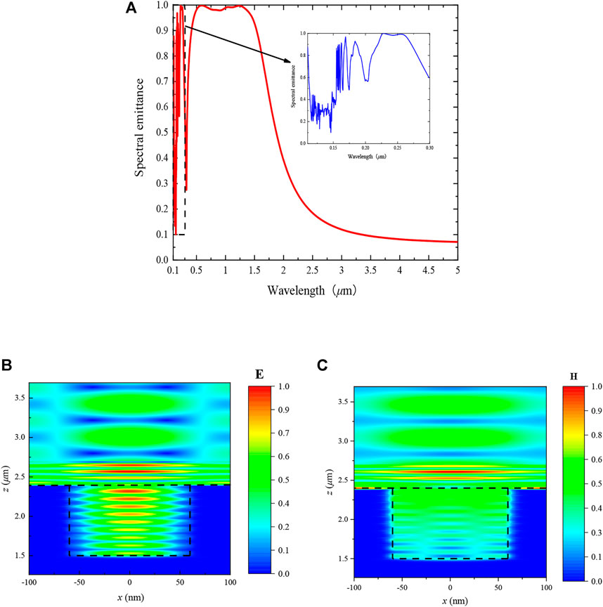
FIGURE 4. (A)Spectral emittance at 0.1–5 μm with structural parameters of LP = 10, r = 60 nm, a = 200 nm, dM = 10 nm, dD = 80 nm, h = 900 nm and (B,C) its normalized electromagnetic fields at λ = 150 nm.
Notably, as shown in Figure 3, the spectral emission bandwidth of the composite structure is broadened compared to that of the one-dimensional structure. To deeply explore the reasons for this phenomenon, it is necessary to understand the reasons for the resonant emission of the composite structure in the wave band of 0.3–2.4 μm. Therefore, we calculated the normalized electromagnetic field cloud at λR1 = 554 nm, λR2 = 947 nm, λR3 = 1291 nm, λR4 = 1392 nm, and λR5 = 1622 nm, as shown in Figures 5A–J. First, it can be seen that in the band where both the composite and one-dimensional structures exhibit high emission (0.46–1.30 μm), and strong electric field confinement can be found on the surface of the composite structure from Figures 5A,C,E. Due to the cavities, the electric field intensity of the array cavities at λR2 = 947 nm and λR3 = 1,291 nm is higher than that of the layered structure in the non-composite cavity region. It is indicated that the CRs generated by the incident wave at the cavity surface is already stronger than the FP resonance generated at the non-cavity surface at this time. The reason why the incident wave resonates only on the surface of the structure is that for two-dimensional microcavity structures, the band in which the strong intracavity resonance is generated is determined by the physical properties of the structure. The cut-off wavelength of the composite structure for the strong intracavity resonance is at λ = 0.1568 μm, and photons with wavelengths beyond this cut-off wavelength can no longer enter the cavity to form standing waves for multiple resonances, but only resonate with the structure surface (Celanovic et al., 2008). Moreover, it is observed from Figure 3 that in the band where both the composite and 1D structures are in high emission (0.46–1.30 μm), the spectral emittance of the composite structure is also higher than that of the 1D structure, which is attributed to the combined effect of FP resonance and CRs to increase the spectral emission of the structure. Furthermore, as shown in observing Figure 3, it can be seen that the spectral emittance of the one-dimensional structure at λR4 and λR5 is already below 0.7, while the spectral emittance of the composite structure is still close to 1. As can be seen in Figures 5G,I, due to the appearance of the array cavity, the incident wave interacts with the resonant cavity, leading to that the electric field in the cavity appears to be strongly confined and the resonance effect brought by the cavity remains in 1.30–1.62 μm, which results in the emission enhancement.
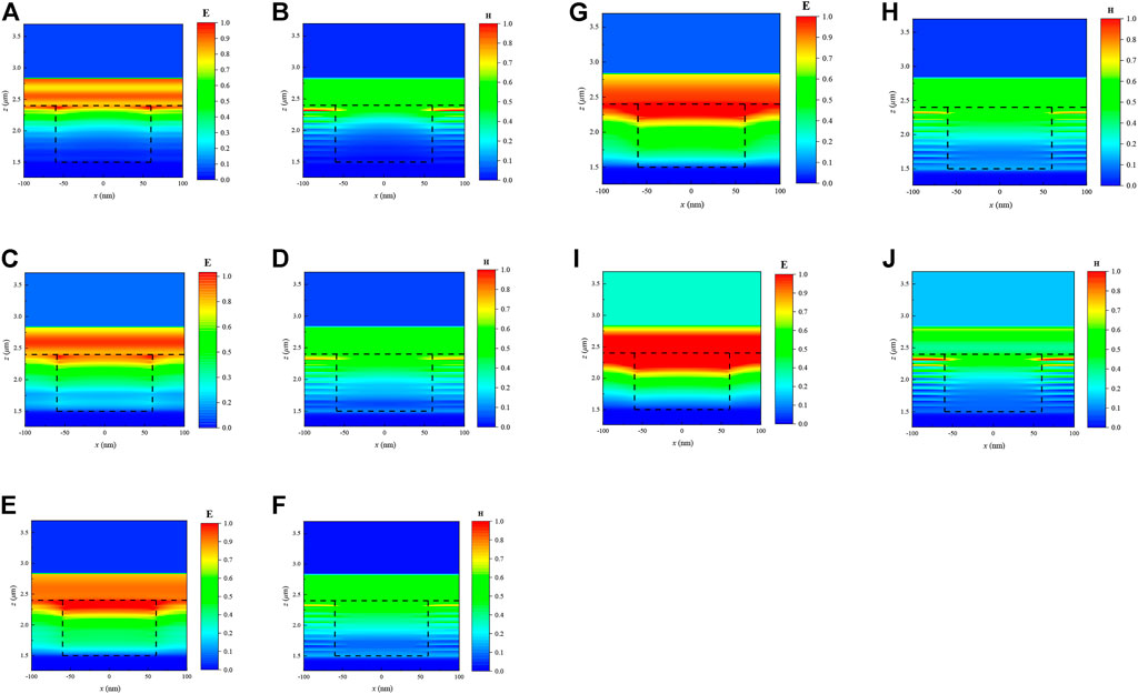
FIGURE 5. Composite structure of LP = 10, r = 60 nm, a = 200 nm, dM = 10 nm, dD = 80 nm, h = 900 nm, and normalized electromagnetic field distribution clouds at λR1 = 554 nm, λR2 = 947 nm, λR3 = 1,291 nm, λR4 = 1,392 nm, λR5 = 1,622 nm, where (A,C,E,G,I) are electric field maps (B,D,F,H,J) are magnetic field maps.
According to previous reports (Zhang et al., 2011; Song et al., 2015), the proposed structural properties excite MPs. MPs are resonances resulting from the coupling of magnetic oscillations on the material surface with incident waves, which mainly depend on the plasma properties and geometrical characteristic parameters of the material (Chen et al., 2011). However, the key factors for the interaction of the incident waves with the structure are the dielectric constant and the magnetic permeability of the medium. The MP resonance location can be predicted by the equivalent LC-circuit model (Zhang et al., 2011), which takes the Mo-HfO2-Mo triple-layered structure according to the geometric model schematic in Figure 1. The equivalent LC circuit diagram was drawn, as shown in Figure 6. LM = 0.5μ0dM indicates the inductance of the dielectric layer separating the two metal layers. Cc = ε0dD (a/2-r)/(a/2+r) is the capacitance of the adjacent upper and lower metals in the x and y directions of the cavity gap, and the capacitance of the separated parallel metal layers is CM = c1εdε0 (a/2)2/dM, where c1 = 0.22 is the numerical factor of the inhomogeneous distribution of the intercavity charge (Khorrami and Fathi, 2019). Due to the nanoscale effect, the presence of drifting electrons in the metal plate affects the total inductance, and thus, the inductance Le = −1/ω2heffε0εM can be adopted to explain the effect of drifting electrons, where ω is the frequency and εM is the metal dielectric function. Because the distribution of the alternating electric field penetrating the metal comes from different sources, the induced current is also distributed in an effective area inside the metal layer. heff is the effective thickness, when δ< dM, heff = δ, otherwise δ = dM, where δ = λ/4πκ is the energy penetration depth and κ is the extinction coefficient of the metal. According to the capacitance-inductance theory model, assuming that Im (Ztot) = 0, the MP resonant frequency of the structure can be predicted by Eq. 12.
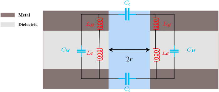
FIGURE 6. MPs resonant equivalent LC circuit model diagram.
The calculation results from Eq. 12 show that the structure can exhibit MPs near λ = 0.3 μm when dM = 10 nm and dD = 80 nm. From Figure 3, it can be seen that the composite structure has an emission peak near 0.3 μm and the magnetic field confinement is observed from the magnetic field diagram in Figure 5B, and thus, the composite structure produces resonant emission due to the excitation of MPs as well.
To sum up, the spectral emission bandwidth of the composite array cavity based on the layered stack structure is wider than that of the layered structure, which is beneficial to improving the output power and efficiency of the system. However, due to the appearance of the array cavity, electromagnetic waves enter the cavity to interact with the layered structure and generate magnetic field confinement with the structure. This phenomenon can increase emittance in the convertible waveband of the TPV cell, leading to a negative impact on the TPV system efficiency. The cavity resonance of the structure is still in line with the prediction of the coupled-mode theory. The intracavity cavity resonance of the structure remains in accordance with the prediction of the coupled-mode theory. The incident wave, after exceeding the cutoff wavelength predicted by coupled-mode theory, does not enter the cavity to generate standing waves to form multiple resonance peaks. Instead, the incident wave forms resonances on the surface of the structure cavity, generating strong electric field confinement and thus increasing the spectral emittance. Hence, the resonant emission of the composite structure in the 0.3–2.4 μm band is due to the combined effect of MPs, CRs, and FP interference effects. MPs have limited contribution to the high emission produced by the structure at 0.3–2.4 μm due to the weak magnetic field confinement. The CRs generated in the cavity of the structure surface and the FP resonance effect generated in the non-cavity region jointly affect the spectral emission characteristics of the structure, and increase the spectral emission rate in the band in the wavelength range of 0.46–1.30 μm. In the wavelength range of 1.3–1.62 μm, the CRs effect does not disappear, and thus, the spectral emission bandwidth is broadened by the CRs and FP resonance effects.
3.3 Influence of geometric feature parameters on spectral tuning performance
3.3.1 Influence of structural layer-pairs
To investigate the effect of different LP (Layer-Pairs, LP) on the optical performance of TPV emitter, the other parameters (r = 60 nm, a = 200 nm, dM = 10 nm, dD = 80 nm, nc = 1) based on typical structural characteristic parameters were fixed, and six different layer-pairs, LP = 5, 6, 7, 8, 9, 10, respectively, were analyzed. Thus, the cavity depths are 450 nm, 540 nm, 630 nm, 720 nm, 810 nm, and 900 nm, respectively. The effect of LP on the normal emittance of the emitter spectrum was analyzed, and the calculated results are shown in Figure 7. According to Eq. 11, the cutoff wavelength of the cavity resonance mode increases with the increase of the cavity depth. As the number of layer pairs increases, the depth of the structural cavity increases with the cutoff wavelength of its spectral emittance. However, it is noteworthy that the cut-off wavelength of the structure spectral emittance no longer changes significantly with increasing cavity depth after the LP is greater than 7 (h = 630 nm). This coincides with the results of the above analysis that cavity resonance occurs only at the surface of the structure. To observe the effect of the array cavity on the spectral emittance of the composite structure obviously, the spectral emittance of the one-dimensional layered structure with different LP as a function of wavelength was calculated. The results are shown in Figure 7B, where dM = 10 nm, dD = 80 nm. It can be seen that the spectral emittance of the one-dimensional structure does not vary much, while for the structure of the composite cavity array, changing the number of layer pairs can modulate the spectral emission characteristics of the structure.
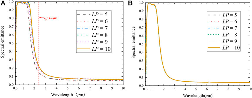
FIGURE 7. (A) Variation of structural spectral emittance with the number of layer pairs for fixed other parameters (r = 60 nm, a = 200 nm, dM = 10 nm, dD = 80 nm, nc = 1), LP = 5, 6, 7, 8, 9, 10 (B) Variation of structural spectral emittance with wavelength (dM = 10 nm, dD = 80 nm) of one-dimensional photonic crystal for different Layer-pairs (LP = 5, 6, 7, 8, 9, 10).
In addition, based on the TPV emitter optical performance evaluation model Eqs 8–10, the normal spectral efficiency at different LPs was calculated, and the results are shown in Table 1. As can be seen, the spectral efficiency does not vary linearly with the emission cutoff wavelength. The main reason is that when the emission bandwidth of the convertible band of the cell increases, the emittance of the non-convertible band also increases, resulting in the improvement in the spectral efficiency by the broadened emission bandwidth being canceled out.

TABLE 1. Normal spectral efficiency corresponding to different layer logarithms (LP = 5, 6, 7, 8, 9, 10).
3.3.2 Influence of nanoarray cavity radius
According to the coupled-mode theory, the cutoff wavelength of CRs is affected by r and h. The effect of h is discussed above, and the effect of r on CRs will be analyzed below. Similarly, the spectral emittance of the array cavity radius r = 20 nm, 40 nm, 60 nm, 80 nm, 90 nm, and 100 nm was calculated based on typical structural feature parameters, fixing other parameters (a = 200 nm, dM = 10 nm, dD = 80 nm, nc = 1, h = 900 nm), as shown in Figure 8A. It can be seen that the cut-off wavelength of emittance increases with increasing radius in the radiative convertible band of InGaAsSb cells. This result is consistent with the expression of Eq. 11, i.e., when the cavity depth is fixed, the cutoff wavelength increases with the increase of the radius. In the radiation non-convertible band of InGaAsSb cells, the spectral emittance also increases with increasing radius, and the average emittance in the non-convertible band is 0.085 when r = 20 nm and reaches 0.295 when r = 100 nm. To investigate the reason for the increase of spectral emittance with increasing radius in the non-convertible band, the normalized electromagnetic fields at λ = 6 μm were calculated for r = 20 nm and r = 90 nm, respectively, as shown in Figures 8B–E. It can be seen that the electric field diagrams are almost identical in the unconvertible band when the array cavity radius increases (as shown in Figures 8B,D). It is found that more magnetic confinement appears in the magnetic field diagram when r = 90 nm (Figure 8E), which is mainly due to the fact that more incident waves enter the array cavity to interact with the structure when the radius getting larger, leading to more magnetic confinement within the layered structure in the non-composite array cavity region of the structure.
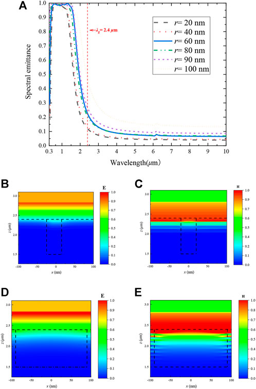
FIGURE 8. (A) Variation of structural spectral emittance with radius (r = 20 nm, 40 nm, 60 nm, 80 nm, 90 nm, and 100 nm) for fixed other parameters of the composite structure (a = 200 nm, dM = 10 nm, dD = 80 nm, nc = 1, h = 900 nm). Normalized electromagnetic field clouds of the composite structure at λ = 6 μm for r = 20 nm (B) electric field (C) magnetic fields and r = 90 nm (D) electric field (E) magnetic fields.
As in the above method, we calculated the spectral efficiency corresponding to different radii, as shown in Table 2. The spectral efficiency of the emitter is lower for a larger cavity radius, which can be attributed to the CRs on the surface of the composite structure. The spectral emission bandwidth increases with the rise of the radius, and the structure is converted from a narrowband emitter to a broadband emitter. However, the spectral efficiency of the broadband emitter can be lower than that of the narrowband emitter (Sakakibara et al., 2019). In the non-convertible band, the incident wave is also more likely to enter the resonant cavity for interaction due to the increased radius. Consequently, the spectral emittance increases due to the magnetic field confinement between the layers of the stack structure, whereas the increased emissivity in the non-conversion band can also reduce the spectral efficiency of the TPV emitter. Therefore, it can be found that when the one- and two-dimensional structures are compounded, the emitter changes from narrow-band to broadband, which is characterized by a higher power output density but a lower spectral efficiency (Burger et al., 2020).

TABLE 2. Normal spectral efficiency corresponding to different radii (r = 20 nm, 40 nm, 60 nm, 80 nm, 90 nm and 100 nm).
3.3.3 Influence of nanoarray cavity period
From Eq. 11, the CRs are affected by the depth and radius of the array cavity for two-dimensional photonic crystals, but the effect of the period on the spectral emittance of the structure is not discussed in the equation. To investigate the effect of the period of the array cavity, other structural characteristic parameters (r = 60 nm, dM = 10 nm, dD = 80 nm, nc = 1, LP = 10, h = 900 nm) were fixed, and the structural spectral emittance was calculated for periods a = 120 nm, 130 nm, 150 nm, 200 nm, 250 nm, and 300 nm, as shown in Figure 9. As can be seen, the emitter emission bandwidth decreases as the period increases. In the convertible band, the radiation of the emitter increases with the decrease of the period of the array cavity. It can be found that the role played by the cavity on the structure incident waves is weakening due to the fact that the larger the period, the less the array cavity per unit area. Accordingly, the spectral emittance of a structure with a larger period is close to that of a one-dimensional structure.
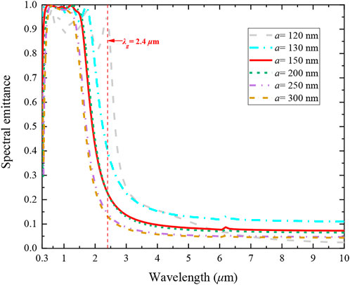
FIGURE 9. Variation of structure spectral emittance with period (a = 120 nm, 130 nm, 150 nm, 200 nm, 250 nm, 300 nm) for fixed composite structure with other parameters (r = 60 nm, dM = 10 nm, dD = 80 nm, nc = 1, LP = 10, h = 900 nm).
Table 3 shows the spectral efficiency corresponding to different periods. It can be seen that the spectral efficiency increases as the period increases. The reason is that the larger the period is, the closer the emission characteristics of the composite structure are to the narrow-band emission characteristics of the one-dimensional structure. According to the literature (Sakakibara et al., 2019), narrow-band emitters can improve spectral efficiency, whereas broadband emitters can produce higher output electric power density.

TABLE 3. Normal spectral efficiency corresponding to different periods (a = 120 nm, 130 nm, 150 nm, 200 nm, 250 nm, 300 nm).
In summary, the emission spectrum of the emitter can be effectively tuned by changing the geometrical characteristics parameters, such as the number of layer-pairs, the radius, and the period of the array cavity. As the number of layer pairs increases, the emission cut-off wavelength of the emitter increases. However, because the CRs of the structure occurs only on the surface, the spectral emittance no longer changes significantly when the number of layer pairs is larger than 7. As the radius increases, the cutoff wavelength increases, as well as the average emittance in the non-convertible band. With the increase of the period, the spectral emission characteristics of the composite structure are similar to those of the one-dimensional layered structure. The reason is that the larger the period is, the fewer the array cavities in the unit area are, and thus, the effect on the spectral emission of the structure is weakened.
3.4 Wide-angle adaptability of the composite structure
Through the above analysis, it can be found that the core parameters affecting the spectral emittance of the composite structure are the number of layer pairs, and the radius and period of the array cavity. To match the InGaAsSb cell, we take the structure parameters as LP = 10, r = 60 nm, a = 150 nm, dM = 10 nm, dD = 80 nm, and nc = 1. Angular control is also an aspect of emitter spectral tuning to ensure spectral control at all angles (incidence angle θ, azimuth angle φ, polarization angle ψ), and the emitter needs to accept photons over a wide range of angles (Sakakibara et al., 2019). To explore the angular control stability of the composite structure emitter under different incidence angles and polarization methods, the directional spectral emittance was calculated for incidence angles θ = 0° and θ = 50° when the incident waves were TE and TM polarized, respectively, as shown in Figure 10.
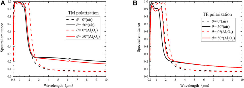
FIGURE 10. The spectral emittance for incident angles θ = 0° and θ = 50° when the incident waves (A) TM and (B) TE are polarized and the array cavity filling media are air and Al2O3, respectively.
To compare the wide-angle stability of the composite structure at a large-angle oblique incidence of the incident wave, the variation of the structure spectral emittance with the incident angle for the one-dimensional structure (dM = 10 nm, dD = 80 nm) and the two-dimensional Mo structure (r = 60 nm, a = 150 nm, h = 900 nm, nc = 1) with TM polarization and TE polarization were calculated, as shown in Figures 11, 12. Regarding the one-dimensional structure, in the convertible band of the cell, when the incident wave is TM polarized, it can maintain high emission at θ ≤ 50°, and the emittance of its high emission band is all greater than 0.95. When TE polarized, the emittance decreases with increasing the incident angle, and the average emittance of the emission band drops to 0.8 at θ = 50°; while in the non-convertible band of the TPV cell, the spectral emittance increases with increasing the incident angle. For the two-dimensional Mo structure, the spectral emittance increases with increasing incidence angle when the TM wave is incident in the convertible ban, and decreases with increasing incidence angle when the TE is polarized; in the non-convertible band of the cell, the spectral emittance increases with increasing incidence angle for both TE and TM wave incidence. It is worth noting that, in combination with Figures 10–12, it can be seen that the spectral emittance in the unconvertible band radiation increases with the increase of the incident angle, regardless of the structure and the polarization mode. The main reason is that at wavelengths greater than the emission cutoff wavelength, and the emitter does not resonate with the incident wave, at which point the electromagnetic properties of the material itself are represented. Therefore, as the incident angle gets closer to the Brewster angle (≈70°), the lower the reflectivity of the incident wave through the dielectric, leading to an increase in spectral emittance, which is consistent with Brewster angle theory (Chubb, 2007).
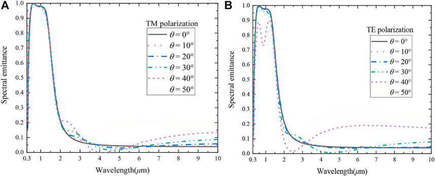
FIGURE 11. Variation of spectral emittance with incident angle for one-dimensional structures (LP = 10, dM = 10 nm, dD = 80 nm) for (A) TM polarization and (B) TE polarization, respectively.
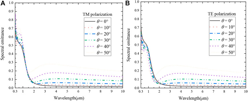
FIGURE 12. Variation of spectral emittance with incident angle for two-dimensional Mo structures (r = 60 nm, a = 150 nm, h = 900 nm, nc = 1) for (A) TM polarization and (B) TE polarization, respectively.
The main reason for the attenuation of the spectral performance of the 2D structured emitters at oblique incidence is that the obliquely incident light is not effectively coupled into the cavity mode, which results in diffraction loss from the structure. Diffraction loss allows free space radiation to be reflected into unwanted diffraction channels. Therefore, to further enhance the wide-angle adaptation of composite structures containing cavity arrays, it is necessary to analyze the effect of diffraction modes on the emittance of photonic crystals and avoid diffraction loss:
where a is the structure period, θ is the plane wave incidence angle, θm is the m th order diffraction angle. When the incident wave is normal to incidence, θ = 0° and a = mλ, while for obliquely incident electromagnetic waves, the m th order diffraction can be determined by Eq. 14.
The effect of the array cavity period on the spectral emission of the structure has been studied above. In the following, the effect of the refractive index of the cavity medium on the spectral emittance will be investigated. Other parameters (LP = 10, h = 900 nm, r = 60 nm, a = 200 nm, dM = 10 nm, dD = 80 nm) are fixed and calculate the spectral emittance when the array cavity filling medium is the high temperature dispersion resistant material W, SiO2, Al2O3 and air, respectively, as shown in Figure 13. In the convertible band, the emitting cut-off wavelength of the emitter increases with the refractive index of the cavity-filling medium, and the emittance does not change significantly after the broadening of the emitting resonance band, the average emittance is greater than 0.9, while in the non-convertible band the emittance changes little. This result shows that the emission resonance is related to the filled cavity medium, while in the long wavelength band non-resonant emission is almost independent of the cavity medium, i.e., it is indicated that the emission in the long wavelength band has a limited relationship with the array cavity and is related to the layered structure, which is consistent with the previously discussed results. It is noteworthy that the filled medium is the spectral modulation performance of W differs greatly from that of SiO2 and Al2O3, which is mainly caused by the difference in their optical constants. When the cavity of the two-dimensional structure is filled with a material with a larger refractive index and better thermal stability, the thermal stability and spectral performance of the emitter can be enhanced (Sakakibara et al., 2018). Thus, we compared spectral emittance when the incident wave TM and TE are polarized and the array cavity filling media are air and Al2O3 for the incident angle θ = 0° and θ = 50°, as shown in Figure 10. To observe the wide-angle stability of the composite structure array cavity before and after filling with Al2O3 more intuitively, the efficiency of the orientation spectrum and its rate of change for the incident wave TM and TE polarization with the incident angle θ = 0° and θ = 50° were calculated, as shown in Table 4. As can be seen, the change rate of the spectral efficiency after filling the array cavity with dielectric Al2O3 is the lowest regardless of TM or TE polarization, indicating that the wide-angle stability can be improved after filling the array cavity with dielectric.
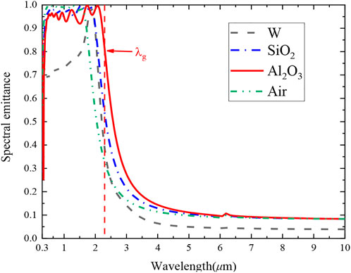
FIGURE 13. With other parameters fixed (LP = 10, h = 900 nm, r = 60 nm, a = 150 nm, dM = 10 nm, dD = 80 nm), the spectral emittance of the structure varies with the filling medium (W, SiO2, Al2O3 and Air).
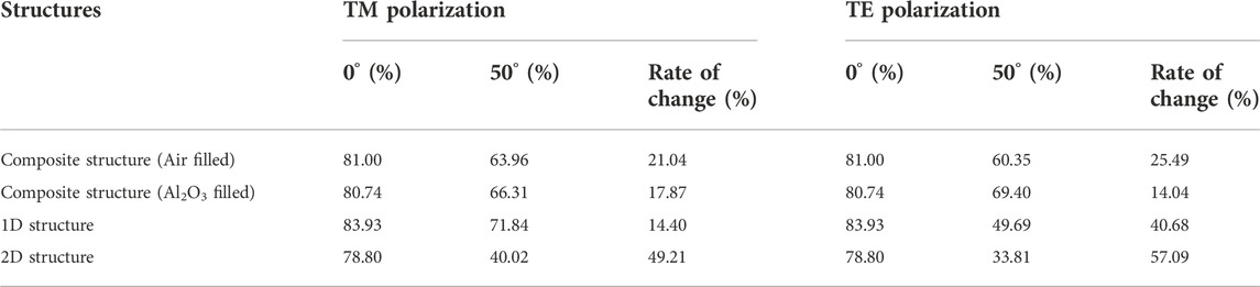
TABLE 4. Spectral efficiency and rate of change of spectral efficiency of composite structure (Air filled and Al2O3 filled), 1D structure and 2D structure for incident wave TM and TE polarization with incidence angle θ = 0° and θ = 50°.
To visualize the wide-angle adaptation of the structures, we calculated the spectral efficiency and the rate of change of optical efficiency for the four structures at incident wave TM and TE polarization with an incidence angle of 0° and 50°, respectively. The calculated results are shown in Table 4. The four structures are composite structure with an air-filled cavity, composite structure with an Al2O3-filled cavity, one-dimensional structure, and two-dimensional structure. It can be seen that the composite structure of the array cavity filled with Al2O3, maintains a low rate of change in spectral efficiency (17.87% and 14.04%, respectively) for both TM and TE polarization. The 1D structure also maintains good wide-angle stability at TM polarization, whereas the TE polarization spectral efficiency variability reaches 40.68% with poor wide-angle stability. In contrast, the two-dimensional structure achieves a spectral efficiency change rate of 49.21% and 57.09% at incident wave TM and TE polarization, respectively, almost losing the originally designed spectral selective performance.
In summary, the 1D structure has better angular adaptation performance and the 2D structure is more prone to coupled mode resonance. The composite structure can still maintain the spectral selectivity at θ ≤ 50° for the incident wave due to the combination of the properties of the 1D and 2D structures, regardless of TM polarization or TE polarization. Other than that, this structure still maintains high emission in the convertible band of the cell. The array cavity of the structure is filled with a high-temperature resistant dielectric to further enhance the wide-angle stability of the emitter. The reason is that the filled dielectric with high-temperature resistance reduces the diffraction loss of the structure. In addition, the emitter does not resonate with the incident wave at wavelengths greater than the emission cutoff. In this case, it reflects the electromagnetic properties of the material itself. Hence, when the incident angle is closer to the Brewster angle (≈ 70°), the lower the reflectivity of the incident wave through the dielectric, resulting in increased spectral emittance.
4 Conclusion
In this work, a multilayer Mo-HfO2 emitter with a composite array cavity structure was proposed, and its emission mechanism and wide-angle adaptability for the application of thermophotovoltaic emitter were deeply analyzed. The origin of the selective emission for the proposed emitter can be attributed to the integrated effect of CRs, FP interference, and MPs. These effects can contribute to increasing average emittance in the cell’s convertible band as well as emission bandwidth. Thus, the system performance can be improved, and the maximum spectral efficiency of the emitter can reach 83.62%. The cut-off wavelength of the composite structured emitter can be fine-tuned by changing the structural layer pairs, radius and period. The cut-off wavelength of structural spectral emittance increases with depth and radius, but decreases with the period. In addition, the structure also exhibits wide-angle adaptability as long as the emission angle is less than 50°.
In conclusion, the combination of one- and two-dimensional structures can circumvent the defects of limited regulation of one-dimensional structures and poor wide-angle stability of two-dimensional, providing a novel guideline for the design of spectrally selective TPV emitters.
Data availability statement
The original contributions presented in the study are included in the article/Supplementary Material, further inquiries can be directed to the corresponding authors.
Author contributions
SC: conceptualization, methodology, software, writing-original draft, visualization. QC: conceptualization, writing-review and editing, resources, investigation. YZ: validation, investigation, data curation, visualization, writing-original draft. QZ: data curation, validation, formal analysis. QY: writing-review and editing, resources. WD: writing-review and editing, data curation. XW: writing-review and editing, supervision, project administration, funding acquisition.
Funding
This work was supported in part by the Natural Science Fund for Colleges and Universities in Jiangsu Province under Grant 19KJB470030, and in part by Open Foundation of State Key Laboratory of Compressor Technology (No. SKL-YSJ201910), and in part by the Key Laboratory of Advanced Carbon Materials and Wearable Energy Technologies of Jiangsu Province MZ26100119, and in part by the Natural Science Foundation of the Jiangsu Higher Education Institutions of China (21KJB470012).
Conflict of interest
Author Qilin Cai was employed by Sunleem Technology Incorporated Company.
The remaining authors declare that the research was conducted in the absence of any commercial or financial relationships that could be construed as a potential conflict of interest.
Publisher’s note
All claims expressed in this article are solely those of the authors and do not necessarily represent those of their affiliated organizations, or those of the publisher, the editors and the reviewers. Any product that may be evaluated in this article, or claim that may be made by its manufacturer, is not guaranteed or endorsed by the publisher.
References
Bani, S., Pan, J., Tang, A., Lu, Q., and Zhang, Y. (2018). Micro combustion in a porous media for thermophotovoltaic power generation. Appl. Therm. Eng. 129, 596–605. doi:10.1016/j.applthermaleng.2017.10.024
Bianchi, M., Ferrari, C., Melino, F., and Peretto, A. (2012). Feasibility study of a Thermo-Photo-Voltaic system for CHP application in residential buildings. Appl. Energy 97, 704–713. doi:10.1016/j.apenergy.2012.01.049
Blandre, E., Shimizu, M., Kohiyama, A., Yugami, H., Chapuis, P.-O., and Vaillon, R. (2018). Spectrally shaping high-temperature radiators for thermophotovoltaics using Mo-HfO 2 trilayer-on-substrate structures. Opt. Express 26 (4), 4346–4357. doi:10.1364/oe.26.004346
Burger, T., Sempere, C., Roy-Layinde, B., and Lenert, A. (2020). Present efficiencies and future opportunities in thermophotovoltaics. Joule 4 (8), 1660–1680. doi:10.1016/j.joule.2020.06.021
Cai, Q., Chen, P., Cao, S., Ye, Q., and Wu, X. (2020). Performance analysis of GaSb cell and thermophotovoltaic system under near-field thermal radiation. Int. J. Thermophys. 41 (12), 161. doi:10.1007/s10765-020-02741-5
Celanovic, I., Jovanovic, N., and Kassakian, J. (2008). Two-dimensional tungsten photonic crystals as selective thermal emitters. Appl. Phys. Lett. 92 (19), 193101. doi:10.1063/1.2927484
Chen, J., Wang, P., Zhang, Z. M., Lu, Y., and Ming, H. (2011). Coupling between gap plasmon polariton and magnetic polariton in a metallic-dielectric multilayer structure. Phys. Rev. E 84 (2), 026603. doi:10.1103/physreve.84.026603
Chou, J. B., Yeng, Y. X., Lenert, A., Rinnerbauer, V., Celanovic, I., Soljačić, M., et al. (2014). Design of wide-angle selective absorbers/emitters with dielectric filled metallic photonic crystals for energy applications. Opt. Express 22 (101), A144–A154. doi:10.1364/oe.22.00a144
Chubb, D. (2007). Fundamentals of thermophotovoltaic energy conversion. Amsterdam, Netherlands: Elsevier.
Dyachenko, P. N., Molesky, S., Petrov, A. Y., Störmer, M., Krekeler, T., Lang, S., et al. (2016). Controlling thermal emission with refractory epsilon-near-zero metamaterials via topological transitions. Nat. Commun. 7 (1), 11809. doi:10.1038/ncomms11809
Farfan, G., Su, M., Taha, M. R., and El-Kady, I. (2010). “High-efficiency photonic crystal narrowband thermal emitters,” in Photonic and phononic crystal materials and devices X (San Francisco, CA: International Society for Optics and Photonics), 76090V.
Fraas, L., Avery, J., and Huang, H. (2003). Thermophotovoltaic furnace–generator for the home using low bandgap GaSb cells. Semicond. Sci. Technol. 18 (5), S247–S253. doi:10.1088/0268-1242/18/5/316
Jiang, C., Shan, S., Zhou, Z., Liang, L., and Huang, H. (2019). Theoretical study of multilayer ring metamaterial emitter for a low bandgap TPV cell. Sol. Energy 194, 548–553. doi:10.1016/j.solener.2019.10.074
Jiang, L., Yuan, C., Li, Z., Su, J., Yi, Z., Yao, W., et al. (2021). Multi-band and high-sensitivity perfect absorber based on monolayer graphene metamaterial. Diam. Relat. Mater. 111, 108227. doi:10.1016/j.diamond.2020.108227
Khodasevych, I. E., Wang, L., Mitchell, A., and Rosengarten, G. (2015). Micro-and nanostructured surfaces for selective solar absorption. Adv. Opt. Mater. 3 (7), 852–881. doi:10.1002/adom.201500063
Khorrami, Y., and Fathi, D. (2019). Broadband thermophotovoltaic emitter using magnetic polaritons based on optimized one-and two-dimensional multilayer structures. J. Opt. Soc. Am. B 36 (3), 662–666. doi:10.1364/josab.36.000662
Kim, J. H., Jung, S. M., and Shin, M. W. (2017). High-temperature degradation of one-dimensional metallodielectric (W/SiO2) photonic crystal as selective thermal emitter for thermophotovoltaic system. Opt. Mater. 72, 45–51. doi:10.1016/j.optmat.2017.05.041
Mandal, P. (2021). Polarization insensitive plasmonic stacked multilayer metasurface with deep nanohole cavity as multi-band absorber. Optik 241, 166959. doi:10.1016/j.ijleo.2021.166959
Molesky, S., Dewalt, C. J., and Jacob, Z. (2013). High temperature epsilon-near-zero and epsilon-near-pole metamaterial emitters for thermophotovoltaics. Opt. Express 21 (101), A96–A110. doi:10.1364/oe.21.000a96
Nguyen-Huu, N., Pištora, J., and Cada, M. (2016). Wavelength-selective emitters with pyramid nanogratings enhanced by multiple resonance modes. Nanotechnology 27 (15), 155402. doi:10.1088/0957-4484/27/15/155402
Papadakis, G. T., Buddhiraju, S., Zhao, Z., Zhao, B., and Fan, S. (2020). Broadening near-field emission for performance enhancement in thermophotovoltaics. Nano Lett. 20 (3), 1654–1661. doi:10.1021/acs.nanolett.9b04762
Rostamnejadi, A., and Daneshvar, M. (2018). Two-dimensional tungsten photonic crystal selective emitter: Effects of geometrical parameters and temperature. Appl. Phys. B 124 (3), 40–48. doi:10.1007/s00340-018-6910-4
Sakakibara, R., Stelmakh, V., Chan, W. R., Ghebrebrhan, M., Joannopoulos, J. D., Soljačić, M., et al. (2018). “Improved omnidirectional 2D photonic crystal selective emitter for thermophotovoltaics,” in Journal of physics: Conference series (Kanazawa, Japan: IOP Publishing), 012056.
Sakakibara, R., Stelmakh, V., Chan, W. R., Ghebrebrhan, M., Joannopoulos, J. D., Soljacic, M., et al. (2019). Practical emitters for thermophotovoltaics: A review. J. Photonics Energy 9 (3), 1. doi:10.1117/1.jpe.9.032713
Silva-Oelker, G., Jerez-Hanckes, C., and Fay, P. (2019). High-temperature tungsten-hafnia optimized selective thermal emitters for thermophotovoltaic applications. J. Quantitative Spectrosc. Radiat. Transf. 231, 61–68. doi:10.1016/j.jqsrt.2019.04.008
Silva-Oelker, G., Jerez-Hanckes, C., and Fay, P. (2018). Study of W/HfO 2 grating selective thermal emitters for thermophotovoltaic applications. Opt. Express 26 (22), A929–A936. doi:10.1364/oe.26.00a929
Song, J., Han, J., Choi, M., and Lee, B. J. (2022). Modeling and experiments of near-field thermophotovoltaic conversion: A review. Sol. Energy Mater. Sol. Cells 238, 111556. doi:10.1016/j.solmat.2021.111556
Song, J., Si, M., Cheng, Q., and Luo, Z. (2016). Two-dimensional trilayer grating with a metal/insulator/metal structure as a thermophotovoltaic emitter. Appl. Opt. 55 (6), 1284–1290. doi:10.1364/ao.55.001284
Song, J., Wu, H., Cheng, Q., and Zhao, J. (2015). 1D trilayer films grating with W/SiO2/W structure as a wavelength-selective emitter for thermophotovoltaic applications. J. Quantitative Spectrosc. Radiat. Transf. 158, 136–144. doi:10.1016/j.jqsrt.2015.02.002
Ulaby, F. T., Michielssen, E., and Ravaioli, U. (2015). Fundamentals of applied electromagnetics. Upper Saddle River, NJ: Pearson.
Wang, L., and Zhang, Z. (2012). Wavelength-selective and diffuse emitter enhanced by magnetic polaritons for thermophotovoltaics. Appl. Phys. Lett. 100 (6), 063902. doi:10.1063/1.3684874
Yang, H.-W., Yang, Z.-K., Pei, Y.-K., and Hao, J.-J. (2017). Simulation and imaging using ultrawideband ground penetrating radar and finite-difference time-domain method. J. Electron. Imaging 26 (5), 1. doi:10.1117/1.jei.26.5.053015
Ye, H., Wang, H., and Cai, Q. (2015). Two-dimensional VO2 photonic crystal selective emitter. J. Quantitative Spectrosc. Radiat. Transf. 158, 119–126. doi:10.1016/j.jqsrt.2015.01.022
Yeng, Y. X., Ghebrebrhan, M., Bermel, P., Chan, W. R., Joannopoulos, J. D., Soljačić, M., et al. (2012). Enabling high-temperature nanophotonics for energy applications. Proc. Natl. Acad. Sci. U. S. A. 109 (7), 2280–2285. doi:10.1073/pnas.1120149109
Zhang, Y., Zhang, Q., Cai, Q., Ye, Q., and Wu, X. (2022). Thermal degradation of the multilayer Mo/HfO2 emitter induced by the oxygen diffusion at high temperature in vacuum. Int. J. Heat Mass Transf. 185, 122425. doi:10.1016/j.ijheatmasstransfer.2021.122425
Zhang, Z., Park, K., and Lee, B. J. (2011). Surface and magnetic polaritons on two-dimensional nanoslab-aligned multilayer structure. Opt. Express 19 (17), 16375–16389. doi:10.1364/oe.19.016375
Zhao, B., Wang, L., Shuai, Y., and Zhang, Z. M. (2013). Thermophotovoltaic emitters based on a two-dimensional grating/thin-film nanostructure. Int. J. Heat Mass Transf. 67, 637–645. doi:10.1016/j.ijheatmasstransfer.2013.08.047
Keywords: thermophotovoltaic systems, wavelength-selective emission, one-dimensional emitters, two-dimensional emitters, electromagnetic resonance
Citation: Cao S, Cai Q, Zhang Y, Zhang Q, Ye Q, Deng W and Wu X (2023) Emission mechanism and wide-angle adaptability of selective emitter based on combination of one and two-dimensional photonic crystals. Front. Energy Res. 10:995782. doi: 10.3389/fenrg.2022.995782
Received: 16 July 2022; Accepted: 22 September 2022;
Published: 06 January 2023.
Edited by:
Linshuang Long, University of Science and Technology of China, ChinaReviewed by:
Song Lv, Wuhan University of Technology, ChinaShimin Li, North University of China, China
Copyright © 2023 Cao, Cai, Zhang, Zhang, Ye, Deng and Wu. This is an open-access article distributed under the terms of the Creative Commons Attribution License (CC BY). The use, distribution or reproduction in other forums is permitted, provided the original author(s) and the copyright owner(s) are credited and that the original publication in this journal is cited, in accordance with accepted academic practice. No use, distribution or reproduction is permitted which does not comply with these terms.
*Correspondence: Qilin Cai, cWxjYWlAc3VkYS5lZHUuY24=; Xi Wu, d3V4aUBzdWRhLmVkdS5jbg==