 Xiangjian Meng
 Jiaxin Liu
 Gongke Wang
 Jingyang Fang
95% of researchers rate our articles as excellent or good
Learn more about the work of our research integrity team to safeguard the quality of each article we publish.
Find out more
ORIGINAL RESEARCH article
Front. Energy Res. , 22 July 2022
Sec. Solar Energy
Volume 10 - 2022 | https://doi.org/10.3389/fenrg.2022.930471
This article is part of the Research Topic Smart Solar Photovoltaic Inverters with Grid-Supportive Services View all 9 articles
High-voltage photovoltaic (PV) techniques have their own advantages in PV plants for reducing the construction cost and improving the operational efficiency. However, the high input PV voltage increases the mismatch losses of PV arrays, which is also a key factor that influences the energy yield of PV plants. This paper proposes a three-input central capacitor (TICC) dc/dc converter for a high-voltage PV system, where four low-rating cascaded buck-boost converters connect to the series-connected three low-voltage PV arrays and two capacitors and realize the maximum power point tracking independently. Meanwhile, there is a neutral point in the proposed converter, enabling it to be connected with the rear-end three-level inverter directly. It can also help balance the three-level dc-link voltage by properly regulating the transferred energy among three input sources. Compared with other transformer-less dc-dc converters, the proposed converter is able to reduce the semiconductor voltage/current stress and therefore achieve the high efficiency. Simulation and experimental results verified the performance of the proposed TICC converter.
Nowadays, the insulation level of PV panels has been developed to reach 1,500 V or even higher to improve the operational efficiency and reduce the construction cost of PV plants. It is claimed that the increment of PV maximum voltage from 1,000 to 1,500 V can lead to 15%–85% saving in conductor mass of cables and 25%–60% saving in the number of combiner boxes (Gkoutioudi et al., 2013). In addition, a high efficiency can be achieved by the reduced current on the dc bus and ac output and the larger operational range of inverters (Serban et al., 2015). However, the increased voltage level also brings some problems. In specific, the high-input PV voltage results in large mismatch power losses among PV panels caused by shadows, manufacturing tolerances, dirtiness, and so on (Kjaer et al., 2005). In addition, the high dc-link voltage leads to high voltage stress on semiconductor devices and a high common mode voltage, especially in the traditional two-level converters.
Currently, there are three widely used grid-tied PV inverters, which are the centralized inverter, the string or multi-string inverter, and the ac module or the module integrated converter (MIC) (Moghadasi et al., 2018). Among these converters, the centralized inverter and string or multi-string inverter are widely used in large-scale PV plants. Centralized inverters are usually connected to several PV arrays, each of which consists of many PV panels connected to the inverter dc-link, which is simple, reliable, and efficient (Karanayil et al., 2019). However, this configuration can only provide a single MPPT operation, and hence, it will increase the mismatch loss with the increment of PV panels in series. Thus, although the insulation voltage level of PV panels has reached 1,500 V, the voltage of PV strings may not be suitable to reach such a high voltage level. Therefore, there is usually a trade-off between the voltage level and mismatch losses. Some works have been carried out to solve this problem (Park et al., 2013; Choi et al., 2015; Choudhury et al., 2016; Karanayil et al., 2019; Yan et al., 2019). In specific, a general control scheme for the dual-input three-level inverter shown in Figure 1A was proposed to track the maximum power points (MPPs) of two PV arrays independently (Yan et al., 2019). Moreover, an auxiliary power converter was proposed to operate under serious partial shading to reduce mismatch losses among PV arrays as shown in Figure 1B (Karanayil et al., 2019).

FIGURE 1. (A) Dual-input three-level inverter. (B) Dual-input three-level inverter with an auxiliary power converter. (C) PV-to-PV DPP converter. (D) PV-to-bus DPP converter. (E) PV-to-virtual bus converter.
To improve the energy harnessing ability and reduce the switching voltage, several series differential power processing (DPP) architectures have been proposed (Shenoy et al., 2013; Stauth et al., 2013; Olalla et al., 2015), which are able to achieve the high efficiency by reducing the power rating of converters. As shown in Figures 1C–E, these series DPP architectures can be mainly classified into three groups: PV-to-PV DPP architectures, PV-to-bus architectures, and PV-to-virtual bus architectures. Regardless of the specific DPP architectures, each PV string can operate at its MPP. However, the total output voltage of the DPP converters is determined by the sum of the MPP voltages of all PV strings, which obviously makes DPP converters lack the voltage boost capability.
Another way to increase the voltage level of PV systems without too much PV panels connected in series is to use the two-stage PV systems with the front-end voltage boost capability. It can provide several advantages, such as a high energy yield and flexibility in plant design (Agamy et al., 2014). Although the distributed converters will lead to the decrease in conversion efficiency as well as an increase in cost per unit power as compared with the centralized converters, an annual energy yield gain of 6%–8% can be achieved to compensate the losses and cost of the additional converters (Elasser et al., 2010). In two-stage PV systems, the boost converter is widely used to step up the input PV voltage. Compared with the two-level inverter, the multi-level inverter can reduce the common mode voltage and improve the operational efficiency. Thus, the three-level boost converter can be assumed in front to reduce the voltage stress on semiconductor devices (Jung-Min Kwon et al., 2008; Tofoli et al., 2015). In Abdullah et al., 2014, a five-level diode-clamped inverter with the three-level boost converter was proposed to output a balanced five-level switching voltage, which further reduces the voltage stress.
Although the boost converter and three-level boost converter can step up the input voltage, they are more efficient when their input voltage is close to their output voltage as indicated in Zientarski et al., 2019. However, a higher input voltage means more PV panels in series and thus more mismatch losses. Therefore, it brings a trade-off between the converter efficiency and mismatch loss as the voltage level of the PV system increases. To overcome such a problem, a dual-input central capacitor (DICC) converter as shown in Figure 2A was proposed to simultaneously track two MPPs and then the input voltage of each PV array and semiconductor voltage/current stress of the converter can be reduced (Chen et al., 2017). Moreover, compared with DPP converters, DICC can maintain the dc-link voltage when the PV array voltage varies, which guarantees its energy harnessing ability. However, it is observed that both DPP converters and the DICC converter need an additional dc-link capacitor stage when they are connected to the multi-level rear-end inverters since these topologies have no distinct neutral point.
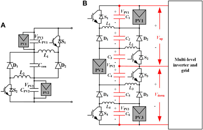
FIGURE 2. (A) Dual-input central capacitor converter. (B) Three-input central capacitor converter.
Being different, this paper proposes a three-input central capacitor (TICC) dc-dc converter, which can track the MPPs of three PV sources independently. It combines the merits of DPP converters and traditional boost converters, reducing the mismatch loss and voltage/current stress as DPP converters and keeping a constant dc-link voltage as boost converters. Besides, it has a distinct neutral point, ensuring that it can be connected to the popular three-level inverter directly. Moreover, by regulating the power transfer of three input PV sources, the proposed converter can help balance the three-level dc-link voltage. The configuration principle of the TICC converter can be extended to build the generalized topologies for involving more PV sources. This paper is organized as follows: Section 2 analyzes the operational principles and scalability of the proposed converter. Then, its control scheme is elaborated in Section 3. After that, a comparative study with its counterparts for high-voltage distributed PV architectures is presented in Section 4. Finally, Matlab simulations and an experiment prototype verified the performance of the proposed dc-dc converter.
The proposed three-input central capacitor converter is drawn in Figure 2B, where six capacitors are in series to power the inversion stage. As a result, the dc-link voltage is divided by the capacitors in series, which reduces the voltage stress on semiconductor devices and provides the necessary neutral point for connecting the rear-end multi-level inverters. Moreover, the output dc voltage Vbus is equal to the voltage sum of six capacitors VCX (X = 1–6), which can be written as
where Vup and Vdown are the upper and lower half parts of the dc bus voltage, respectively. Then, PV sources PV1 and PV3 are parallel with capacitors C1 and C6, respectively, and PV source PV2 is parallel with capacitors C3 and C4, which makes the equivalent input voltage increase 3-fold.
The proposed converter consists of four cascaded buck-boost converters, as illustrated in Figure 3. To distinguish the four buck-boost converters, they are defined as an upper converter, an upper central converter, a lower central converter, and a lower converter from top to bottom. The upper converter and lower converter can regulate the output power of PV1 and PV3, respectively. Moreover, the upper central and lower central converters could regulate the output power of PV2 together.
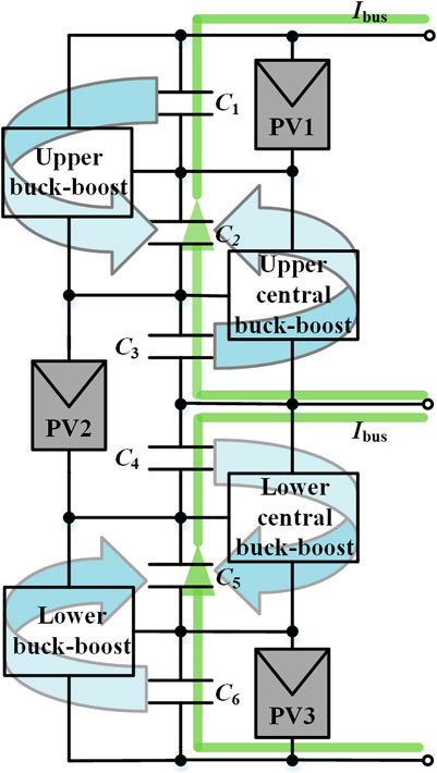
FIGURE 3. Power flow diagram of the proposed converter.
As shown in Figure 3, each buck-boost converter transfers part of the output power of PV sources to the central capacitor C2 and C5. Moreover, the central capacitor discharges its energy by the dc-bus current Ibus. As long as the charging energy and discharging energy of the central capacitors C2 and C5 are balanced dynamically, the voltage of central capacitors can be well regulated. Therefore, the voltage of the central capacitor can vary as the output voltage of the PV source changes, and then the proposed converter can keep a constant dc-bus voltage, which distinguishes it from DPP converters. When the converter operates under CCM conditions, the relationship between the inductor currents and bus current can be calculated as
where dx (x = 1–4) is the duty cycle of switch Sx (x = 1–4). The voltage gain under CCM can be calculated as
Therefore, the output dc voltage Vbus can be expressed as
where VPV1 and VPV3 are the output voltages of PV sources PV1 and PV3, which are equal to VC1 and VC6, respectively, and VPV2 is the output voltage of PV source PV2, which can be calculated as
The DCM of the proposed converter differs from CCM by having an extra interval during each switching cycle when the instantaneous inductor current reaches zero. The boundary condition between CCM and DCM is attained as follows:
where Vin is the input voltage on the capacitor of each buck-boost converter, and fsw represents the switching frequency of the transistor. Like the buck-boost converter, DCM is likely to happen under low power and low inductance value conditions. The boost ratio under DCM can be expressed as
where Req = Vbus/Ibus = Vbus2/(3VPVIPV), representing the equivalent load resistance of the inversion stage.
In addition, the DCM operation announces the merit of lower switching loss. Under DCM conditions, the transistors turn ON under zero current switching (ZCS), and also, the diodes turn OFF under ZCS. The reverse recovery current of the diode is well eliminated because the falling rate of diode current is limited by the inductor.
The three PV sources usually have the same specifications. However, in practice, their output power may be different and time-variant due to the variation of irradiance and some other factors, which can be expressed as
where Pmax is the maximum rated output power of PV sources. During operation, the output power of upper and lower half parts of the TICC converter should be balanced dynamically to make Vup equal Vdown, respectively, which can be achieved by properly regulating four independent switches. In specific, there are 16 switching combinations in total as listed in Table 1. Because the upper converter and the lower converter can work independently, the switching combinations of the proposed converter are then divided into four states according to the working states of the upper central and lower central converters, which need to coordinate with each other to regulate the output power of PV2 and balance the dc-bus voltage.

TABLE 1. Main operational states of the proposed converter.
State 1: Both S2 and S3 are turned ON. PV2 charges inductors L2 and L3, as shown in Figure 4A.
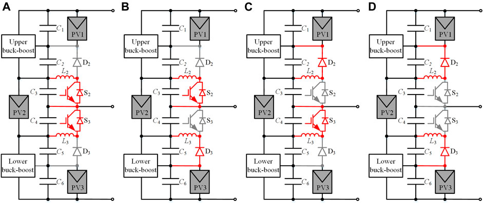
FIGURE 4. (A) State 1, (B) state 2, (C) state 3, and (D) state 4 of the proposed converter.
State 2: Only S2 is turned ON. The energy from PV2 is stored in L2, and inductor L3 discharges its energy to the central capacitor C5, as shown in Figure 4B.
State 3: Only S3 is turned ON. The energy from PV2 is stored in L3, and inductor L2 discharges its energy to the central capacitor C2, as shown in Figure 4C.
State 4: Both S2 and S3 are turned OFF. Inductors L2 and L3 discharge their energy to C2 and C5, respectively, as shown in Figure 4D.
It can be seen from State 2 and State 3 that the upper central converter and lower central converter can deliver differential power to capacitors C2 and C5, respectively. In specific, powers PC3 and PC4 absorbed by the upper central converter and lower central converter, respectively, from PV source PV2 can be expressed as
Therefore, when the voltages on capacitors C3 and C4 are different, the upper central converter and lower central converter can send differential energy to capacitors C2 and C5, respectively, to balance the output voltage. In specific, the relationship between PC3 and PC4 should satisfy the following equation:
Thus, the dc-link voltage can be balanced by regulating the power difference Pdif between PC3 and PC4, which can be derived as
where VC3 and VC4 can be expressed as
Then, the power difference Pdif can be further calculated as
Because VPV1 is approximately equal to VPV3 and Vup is approximately equal to Vdown, the Eq. 13 can be simplified as
Thus, the upper central converter and lower central converter can help balance the power difference between PPV1 and PPV3 by regulating the difference between d2 and d3, and then the proposed converter can output a balanced three-level dc-bus voltage. The input power of PV2 can be derived as
Similarly, the Eq. 15 can be simplified as
Then, the sum of d2 and d3 can also help regulate the output power of PV2. Thus, the proposed converter can regulate the power of three PV sources and balance the three-level dc-link voltage.
Under normal conditions, where the power difference among three PV sources is small, the upper converter and the lower converter can track the MPPs of PV1 and PV3, respectively. The upper central converter and the lower central converter can track the MPP of PV2 together and compensate the power difference between PPV1 and PPV3, as illustrated in Figure 5A.
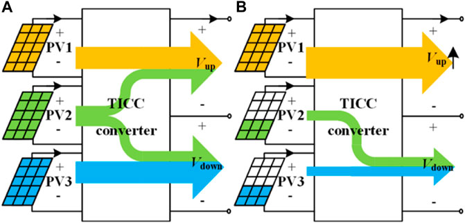
FIGURE 5. Power flow diagrams of the TICC converter (A) when PV2 can compensate the power difference between PV1 and PV3 and (B) when PV2 cannot compensate the power difference between PV2 and PV3.
However, under some extreme conditions, where there is a large power mismatch among three PV sources as shown in Figure 5B, the unbalance of three-level dc-link voltage may occur. In specific, the proposed converter cannot keep a balanced output voltage when the power difference between PPV1 and PPV3 is larger than PPV2, which can be expressed as
However, fortunately, the rear-end three-level inverter can help balance the output voltage of the proposed converter by regulating its PWM sequences (Lyu et al., 2015; Rivera et al., 2015; Tan et al., 2016). In such a case, PV2 sends all its power to compensate the power difference between PPV1 and PPV3, as shown in Figure 5B. The rest power difference is compensated by the rear-end three-level inverter, whose ability to balance the dc bus voltage varies with the different methods. For example, the method presented in Rivera et al., 2015, which used the SVM for the NPC inverter, can achieve the compensation ability as shown in the shaded area of Figure 6, which can be expressed as
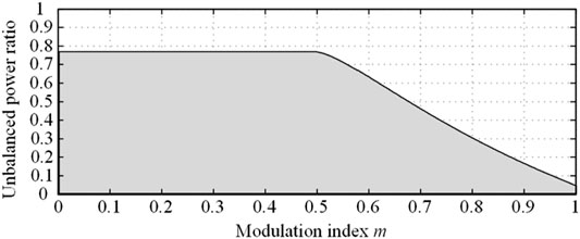
FIGURE 6. Voltage balance limit of the NPC inverter using SVM.
Here, ηn is the limit of the maximum unbalanced power ratio between the unbalanced power and the output power, α is the maximum voltage drift that can be minimized by redistributing the dwell time allocation for redundant small vectors, and m is the modulation index of the NPC inverter. Thus, the NPC inverter can balance the dc bus voltage when the unbalanced power ratio is lower than the limit as expressed below:
Therefore, even if any PV source suffers a permanent damage, the other two PV sources can still work well as long as the Eq. 19 is satisfied. When the three-level inverter is unable to balance the output voltage because the inverter needs more freedom to improve the grid-side current quality (Yaramasu and Wu, 2014) or the unbalanced power ratio is higher than the limit, a non-maximum power point tracking (non-MPPT) algorithm (also known as constant power generation) (Vekic et al., 2017; Liu et al., 2018; Tafti et al., 2018) is enabled to reduce the output power of PV1 or PV3 by forcing it to track the given power references.
To further extend the generalization of the proposed converter configuration, two methods are presented here to scale up the number of PV sources. The first method is to replace each PV source in the TICC converter with a DPP converter, as shown in Figure 7, whose advantage is that it can decouple the control of the TICC converter and each DPP converter, which is beneficial to the modular design. The second method is to embed four PV-to-PV DPP converters to the TICC converter as shown in Figure 8, which can also be seen as embedding two central capacitors in a PV-to-PV DPP converter. It is noted that there is a direct power exchanging path between the upper half part and the lower half part in Figure 8, which can help balance the dc-link voltage, and then the converter can output the qualified three-level voltages. The detailed operational principle of Figure 7 and Figure 8 will not be comprehensively elaborated because they are out of the scope of this paper.
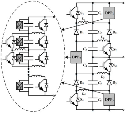
FIGURE 7. Extended configuration of the TICC converter where each PV source is replaced with the DPP converter.

FIGURE 8. Extended configuration of the TICC converter where four PV-to-PV DPP converters are embedded.
In each sampling period, the output power of each PV source and the voltage balance limit ηn are calculated to allocate the balancing task between the proposed converter and the rear-end three-level inverter. The flow chart of their coordinated control scheme is demonstrated in Figure 9A.
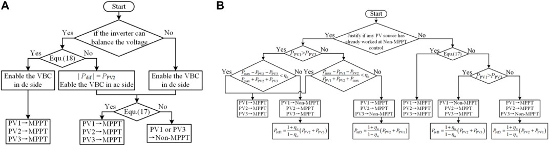
FIGURE 9. Flow chart of (A) coordinated control scheme between the proposed converter and the rear-end inverter. (B) Switching the control mode of each PV source and generating its power reference at non-M.
When the inverter cannot balance the dc-link voltage or PPV2 is enough to compensate the power difference between PPV1 and PPV3, which can be expressed as an Eq. 20
the voltage balance control (VBC) in the dc side is responsible to balance the dc-link voltage. Otherwise, the VBC in the ac side is enabled to help balance the dc-link voltage and all the output power of PV2 is sent to compensate the power difference between PPV1 and PPV3 in the dc side. Therefore, the power difference Pdif between PC3 and PC4, which determines the compensated power provided by PV2, can be calculated as
Then, if the unbalanced power ratio is within the maximum voltage balance limit ηn as expressed in the Eq. 19, the VBC in the dc side or ac side can keep a balanced dc-link voltage when three PV sources work at their MPPs. Otherwise, PV1 or PV3 is forced to operate at the non-MPPT mode and track the given power reference until the possible maximum unbalanced power ratio is reduced to the voltage balance limit. The flow chart of switching the control mode of each PV source and generating its power reference at non-MPPT control is shown in Figure 9B. When the power difference of three PV sources is lower than the limit of the maximum unbalanced power ratio of the NPC inverter ηn as indicated in Eq. 19, the three PV sources can all work at the MPPT mode. Otherwise, the non-MPPT mode of PV1 or PV3 is enabled to balance the dc-link voltage. The power reference of the PV source at the non-MPPT mode can be calculated by
Then, it can return to the MPPT mode until the possible maximum unbalanced power ratio is reduced to the voltage balance limit. The possible maximum unbalanced power ratio is given by
where Pmax is the maximum output power of PV sources.
Figure 10A shows the control scheme of the upper central and lower central converters. The P&Q method is used to track the MPP of PV source PV2 and provides the voltage reference VPV2_ref (Qian Zhang et al., 2014). A double-loop control strategy is applied to control the converters (Tan and Middlebrook, 1995), in which the outer loop regulates the output voltage of PV2 by generating the current reference iLref and the inner loop regulates the average current of iL2 and iL3 and balances the dc-link voltage. A voltage balance component Δd is introduced to regulate the power difference between PC3 and PC4. When the VBC in the dc side is responsible to balance the dc-link voltage (Kim et al., 2018), Δd is given by the Eq. 24
where kpbalance is the proportional gain of the controller. As demonstrated in Section 2.1, the difference between d2 and d3 plays an important role in regulating Pdif. The relationship between duty ratios d2 and d3 can be calculated as
Then, Δd can be used to regulate Pdif and is proportional to the difference between Vup and Vdown, which therefore can be used to balance the three-level dc-link voltage. The sum of d2 and d3 can determine the value of PPV2, which can be calculated as
where D is the deviation between the current reference iLref and the average current of iL2 and iL3. Therefore, D can be used to control PPV2.
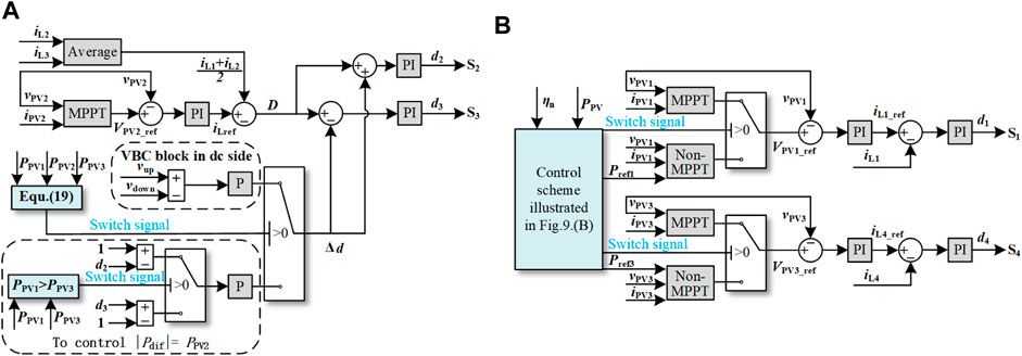
FIGURE 10. (A) Control scheme of the upper central and lower central converters. (B) Control scheme of the upper and lower converters.
While the VBC in the ac side is enabled to balance the dc-link voltage, the power difference Pdif between PC3 and PC4 need to equal PPV2. Because the sum of PC3 and PC4 equals PPV2, PC3 and PC4 can be calculated as
It can be seen from the Eq. 9 and Eq. 12 that PC3 and PC4 decrease to 0 when d2 and d3 increase to 1. Thus, to make Pdif equal PPV2, PC3 or PC4 needs to decrease to 0 by controlling d2 or d3. Then, the voltage balance component Δd can be calculated as
where kp is the proportional gain of the controller.
The upper and lower converters also employ the double-loop control strategy, as shown in Figure 10B. The control scheme shown in Figure 9B is used to switch the control modes of PV1 and PV3 between the MPPT control and non-MPPT control. Then, the outer loop regulates the output power of PV sources by controlling their output voltage, and the inner loop controls the inductor current iL by providing the duty cycle to the switch.
There are several methods for PV sources to track the given power references (Vekic et al., 20172017; Liu et al., 2018; Tafti et al., 2018). Among them, the non-MPPT algorithm described in Liu et al., 2018 is used in this paper, whose flowchart is shown in Figure 11, where the comparison of dP/dU with zero is performed first to make a distinction between states in the unacceptable zone (left from the MPP) and desired zone (right from the MPP) (Vekic et al., 20172017). Then, a variable step ΔP is employed to reduce both the overshoot of the dc-link voltage and the active power oscillations, which reduces its value when Pk is close to Pref. a is the coefficient of the power point tracking step.
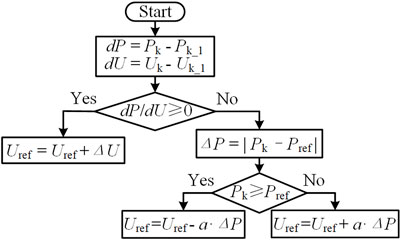
FIGURE 11. Flowchart of the non-MPPT algorithm.
To evaluate the properties of the proposed converter, its performance has been compared with its counterparts including the traditional boost converter, interleaved boost converter, three-level boost converter, and dual-input central capacitor converter.
The device quantity of the proposed converter and its counterparts has been compared from the aspects of total and average device quantity as listed in Table 2. The average device quantity is the ratio of total device quantity over the quantity of PV sources. It can be observed that although the total device quantity of the proposed converter increases, the average device quantity of the proposed converter is less than or almost equal to those of its counterparts.
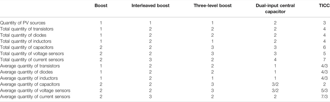
TABLE 2. Comparison of device quantity.
When the proposed converter operates under CCM and the output power and voltage of three PV sources are equal, the relationship between the input PV voltage VPV and the output voltage Vbus can be derived from Eq. 29
Also, when the output power and voltage of three PV sources are equal, the power transferred from PV1 and PV3 to the central capacitors is equal and PV2 transfers equal power to the central capacitor C2 and C5. Thus, the power transferred from PV1 to C2 is twice the power transferred from PV2 to C2. According to the method of power balance on the central capacitor C2, the following equation can be derived:
where VC2 can be calculated as
and VC1 and VC3 can be calculated as
Thus, the average currents through S1 and S2 can be calculated as
Because the switches only conduct during turn-on intervals, their peak current stresses can be calculated as
Here, the inductor current ripple has been neglected for simplicity. Similarly, the average current of diodes D1 and D2 can be expressed as
The processed maximum power of each semiconductor device can be derived by multiplying its peak voltage stress by its peak current stress. The comparison of semiconductor device stress is listed in Table 3. It can be seen that the voltage and current stresses of transistors and diodes in the proposed converter are mostly lower than those of its counterparts. Although more devices have been used, the sum of the processed maximum power of all switches and diodes for the TICC converter is the smallest.
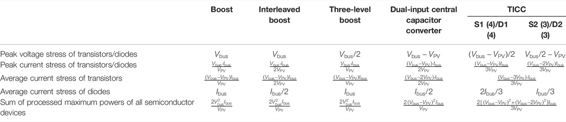
TABLE 3. Comparison of semiconductor device stress.
Figure 12 illustrates the relationship between boost ratio, voltage stress, current stress, and duty ratio when the input voltage VPV equals to 100 V and the current of dc bus Ibus equals to 1 A, where their equations are listed in Table 4.
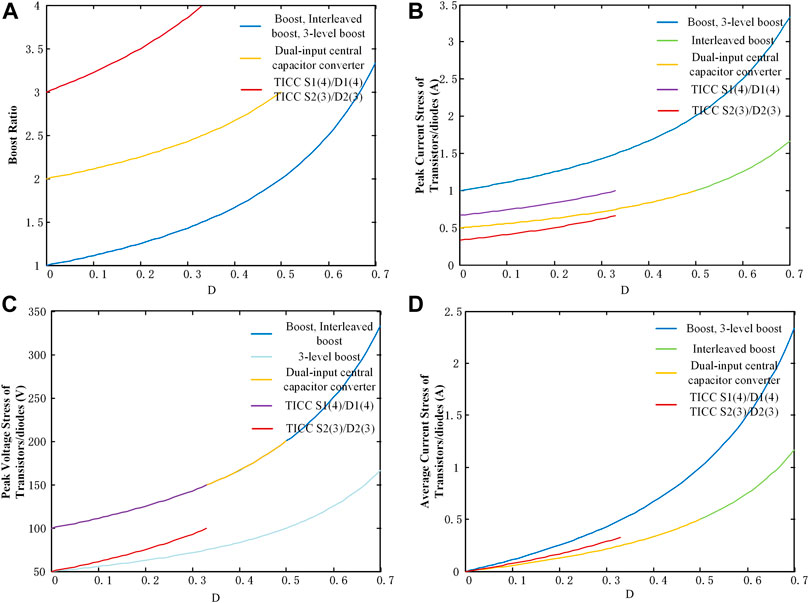
FIGURE 12. (A) Boost ratio, (B) peak current stresses of transistors/diodes, (C) peak voltage stresses of transistors/diodes, (D) average current stresses of transistors/diodes vs. duty ratio.
TABLE 4. Comparison of semiconductor device stress.
It can be seen that the boost ratio has nearly tripled and the peak and average current stresses have been halved, compared with the three-level boost converter. Although the peak voltage stress has nearly doubled when the duty ratio is the same, the voltage stress under the same output voltage is reduced as listed in Table 3.
As analyzed in Dusmez et al., 2015, the three-level boost converter shows its superior efficiency performance over the traditional boost converter and interleaved boost converter. Therefore, to analyze the efficiency performance of the proposed converter, the proposed TICC converter can be only compared with three-level boost (THB) converters shown in Figure 13 under the same input and output conditions. The loss calculation is based on the parameters listed in Table 5. The calculation process of the semiconductor losses is composed of two steps. First, the loss-calculation model for a single device (IGBT or diode), which satisfies the requirement of the maximum conduction current and withstand voltage, is established by using the method of curve fitting to get the function relationship between the collector current and turn-on losses, the function relationship between the collector current and turn-off losses, and so on. Here, a datasheet of the IGBT module from Infineon is used to establish the loss-calculation model (Infineon, 2017). Then, the switching and conduction losses during each switching period can be obtained from the loss-calculation model in Agamy et al., 2014.

FIGURE 13. Three three-level boost converters.
TABLE 5. Parameters for loss calculation.
The semiconductor losses are composed of IGBT’s switching losses and conduction losses, the diode’s reverse-recovery losses, and conduction losses, which can be calculated as
where Pswitch_IGBT and Pcon_IGBT represent the switching and conduction power losses of IGBTs, and Eon (ipeak) and Eoff (ipeak) refer to the turn-on and turn-off energy losses of IGBT, which are the functions of the collector current ipeak that passes through the IGBT. Vsw is the practical switching voltage of the switching process, Vrated is the rated switching voltage of the switching process, and fsw is the switching frequency. Iavg_IGBT and Iavg_diode are the average currents that pass through IGBT and diode, respectively. VCE (ipeak) is the collector-emitter voltage of IGBT, which is the function of the collector current ipeak. Prec_diode and Pcon_diode are the reverse-recovery and conduction power losses of diodes, respectively. Erec (ipeak) is the reverse-recovery energy loss of the diode, which is the function of the forward current ipeak that passes through the diode. VF(ipeak) is the forward voltage of the diode, which is the function of the forward current ipeak.
The inductors can be selected by the software from Magnetics (Kjaer, 2004); then the corresponding losses of the inductor can be expressed as
where Pcore and Pcopper are the core loss and copper loss of the inductor, respectively, which can be calculated as
where Idc is the effective dc current flowing through the inductor, which approximately equals ipeak. Iripple is the high-frequency ripple current, which is usually 30% of the dc current passing through the inductor. Rdc is the dc resistance of the inductor, and L is the inductance that must be maintained by the inductor, which can be calculated as
where Vin is the input charging voltage of the inductor and d is the duty cycle of the charging state of the inductor.
Figure 14A shows the evaluated efficiency of these two converters under different load conditions (10%–100%) as the input voltage varies, indicating a higher efficiency of the proposed TICC converter over the three-level boost converter when their input PV voltages are equal. Here, the capacitor losses are neglected since the equivalent series resistance of the capacitor is usually quite small, for example, dozens of milliohms. With the increment of input PV voltage, the efficiency of the three-level boost converter can be improved. However, it will bring more mismatch power losses between PV modules. Figures 14B–E shows the fractions of power dissipated by the IGBT’s switching, the IGBT’s conduction, the diode’s reverse recovery, and the diode’s conduction operations, respectively. It can be seen that the proposed TICC converter reduces the IGBT switching and conduction losses and the diode’s reverse-recovery losses effectively, compared with three three-level boost converters. In addition, although one more inductor is used, the proposed converter has lower inductor losses as shown in Figure 14F because the currents flowing through the inductors of the TICC converter are low, which reduces its copper loss.
FIGURE 14. (A) Efficiency of the proposed TICC converter and three three-level boost converters, (B) fraction of power dissipated by IGBT’s switching among two converters, (C) fraction of power dissipated by IGBT’s conduction among two converters, (D) fraction of power dissipated by the diode’s reverse recovery among two converters, (E) fraction of power dissipated by the diode’s conducting among two converters, and (F) fraction of power dissipated on the inductor among two converters.
The inductor can be calculated by
where Vin is the input charging voltage of the inductor and d is the duty cycle of the charging state of the inductor. Iripple is the high-frequency ripple current, which is usually 30% of the dc current Idc passing through the inductor. Idc approximately equals ipeak, which is the peak current stress of transistors.
Then the voltage ripple factor KC, which is important when we select the capacitor, can be calculated as
where VC is the capacitor voltage and ΔVC is the voltage ripple, which can be calculated as
There are three states of the central capacitor C2 and C5, as shown in Figure 15. In the first state (0 ∼ d1Ts), the capacitor current IC1 equals the dc bus current Ibus, which can be expressed as
and in the second state (d1Ts ∼ d2Ts), the capacitor current IC2 can be calculated as
where IL1 is the current of inductor L1. In the third state (d2Ts ∼ Ts), the capacitor current IC3 can be calculated as
where IL2 is the current of inductor L2. The inductor currents IL1 and IL2 approximately equal Ipeak, which can be calculated by Eq. 34. Then the voltage ripple on the central capacitor can be calculated as
where D1 and D2 are the conduction duty cycles of switches S1 and S2, respectively. Thus, the central capacitor can be calculated as
and there are two states of the input capacitor, as shown in Figure 16. In the first state (0 ∼ dTs), the capacitor current can be calculated as
In the second state (dTs ∼ Ts), the capacitor current can be calculated as
Then the voltage ripple on the input capacitor can be calculated as
Thus, the input capacitor can be calculated as
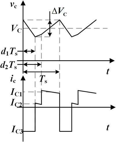
FIGURE 15. Central capacitor voltage and current in the TICC converter.
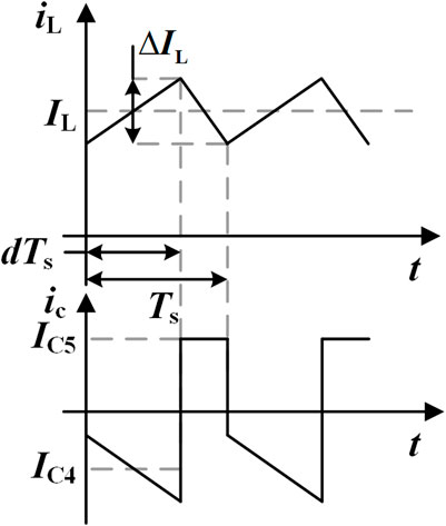
FIGURE 16. Currents of the inductor and input capacitor in the TICC converter.
The Matlab simulation model has been built to verify the performance of the proposed three-input central capacitor converter, whose corresponding circuit parameters are listed in Table 6. To simulate the irradiation variations on the grid-tied PV system, the irradiation level of PV2 varies from 950 W/m2 to 650 W/m2 at the time of 0.05 s and recovers to 950 W/m2 at the time of 0.3 s, while the irradiation levels of PV1 and PV3 keep unchanged at 1,000 W/m2 and 980 W/m2. Figure 17A shows the simulation waveforms. When the irradiation level of PV source PV2 suffers a disturbance, its output power varies with the change of the irradiation level. It can be seen that half of the dc-link voltage is regulated steadily to 600 V and the grid currents are not deteriorated.
TABLE 6. Parameters of the simulation model.
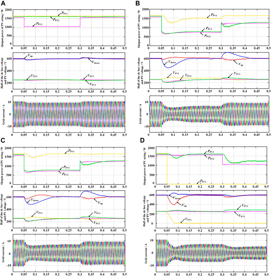
FIGURE 17. (A) Simulated waveforms when the PV2 irradiance declines from 950 W/m2 to 650 W/m2 at 0.05 s and recovers to 950 W/m2 at 0.3 s, (B) simulated waveforms when the irradiation levels of PV2 and PV3 reduce from 950 W/m2 to 450 W/m2 and from 980 W/m2 to 480 W/m2, respectively, at 0.05 s and recover to 750 W/m2 and 780 W/m2, respectively, at 0.3 s, (C) simulated waveforms when the variation of the irradiation level of PV2 and PV3 is the same as that in the previous case, but the inverter is involved to balance the dc-link voltage, and (D) simulated waveforms when the irradiation level of PV1 reduces to 0 W/m2 at 0.05 s and the irradiation level of PV2 reduces by 300 W/m2 at 0.3 s.
Another scenario is defined to evaluate the performance of the proposed converter under non-MPPT control by disabling the dc-link voltage regulation capability of the rear-end inverter. The irradiation levels of PV2 and PV3 reduce from 950 W/m2 to 450 W/m2 and from 980 W/m2 to 480 W/m2, respectively, at the time of 0.05 s and recover to 750 W/m2 and 780 W/m2, respectively, at the time of 0.3 s, while the irradiation level of PV1 keeps unchanged at 1,000 W/m2. At the time of 0.05 s, the output power of PV1 is higher than the sum of the output powers of PV2 and PV3, which enables the non-MPPT control of PV1. As a result, the output voltage of PV1 is controlled to rise up in order to reduce its output power. It can be seen that the output power of PV1 is then kept to a constant value, which equals the sum of the output powers of PV2 and PV3. Therefore, the three-level dc-bus voltage can still keep balanced as shown in Figure 17B. Moreover, at the time of 0.3 s, the sum of the output powers of PV2 and PV3 is larger than the maximum output power of PV1 and then PV1 recovers to MPPT control. The output power of PV1 recovers to the initial level. Thus, the proposed converter can balance the dc-link voltage independently.
The next case is to verify the performance of the coordinated control between the proposed converter and the rear-end three-level inverter when the unbalanced power ratio is lower than the power balance limit, where the variation of the irradiation level of three PV sources is the same as that in the previous case, but the inverter is able to balance the dc-link voltage. Although the output power of PV1 is higher than the sum of the output powers of PV2 and PV3 at the time of 0.05 s, the three PV sources can still work at their MPPs because the inverter can help balance the dc-link voltage, as shown in Figure 17C. Then at the time of 0.3 s, the output power of PV2 and PV3 increases with the variation of the irradiation level.
Finally, to show the performance of the proposed converter when any PV source suffers a permanent damage, the irradiation level of PV1 reduces to 0 W/m2 at the time of 0.05 s and the irradiation level of PV2 reduces from 950 W/m2 to 650 W/m2 at the time of 0.3 s, while the irradiation level of PV3 keeps unchanged at 980 W/m2. It can be seen from Figure 17D that PV2 and PV3 can still work at their MPPs before the time of 0.3 s, where the unbalanced power ratio is within the power balance limit. Here, the power balance limit is defined as 0.08. At the time of 0.3 s, a further decrease of the irradiation level of PV2 causes that the unbalanced power ratio exceeds the power balance limit. Therefore, the non-MPPT control of PV3 is enabled to track the given power reference and help balance the dc-link voltage. As shown in Figure 17D, the non-MPPT control and the VBC in the ac side can coordinate well to balance the dc-link voltage.
To further evaluate the performance of the proposed converter, an experimental prototype was built as shown in Figure 18, whose component values and circuit parameters are listed in Table 7. All control algorithms are programmed in a DSP TMS320F28335 from TI and an FPGA XC3S500E. Three independent PV strings are connected in front. Since the irradiance level cannot be flexibly controlled for the installed rooftop PV strings, this experimental prototype can only examine the steady-state operation and the transient operation where PV voltage references suffer sudden changes.
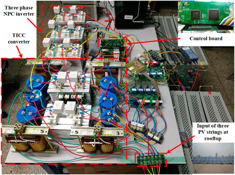
FIGURE 18. Experimental testbed.
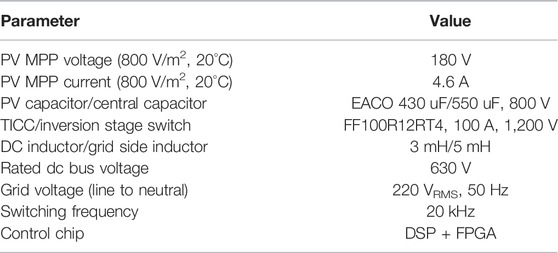
TABLE 7. Parameters of the experimental prototype.
Figure 19A shows the experimental results when the PV voltage reference suffers a sudden decline to examine the PV voltage tracking and dc-link voltage balancing capability of the proposed converter. The voltage reference of PV1 is reduced from 180 V to 150 V at instant t1. It can be seen that the dc-link voltage can keep balanced automatically, and the grid voltage and grid currents are in phase. Figure 19B shows the experimental waveforms when the PV2 voltage reference rises up from 180 V to 190 V at instant t2. After a transient process, half of the dc-link voltage can be regulated to the steady-state value of 315 V, guaranteeing the normal operation of the rear-end inverter.
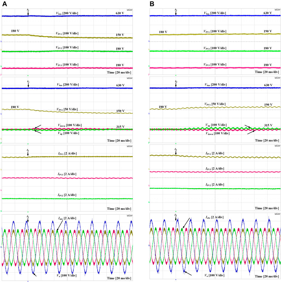
FIGURE 19. Experimental waveforms when (A) PV1 reference declines from 180 V to 150 V at instant t1 and (B) PV1 reference rises up from 180 V to 190 V at instant t2.
To analyze the efficiency performance of the proposed converter, the proposed TICC converter is compared with three-level boost converters shown in Figure 20. Because it is difficult to evaluate the mismatch loss at different input voltages, they are compared under the same input and output conditions. The input PV strings are replaced with the dc sources to adjust the output power flexibly. Then, with the input voltage of 250 V and the output dc-link voltage of 1,000 V, the efficiencies of the proposed TICC converter and three-level boost converters under different input power conditions are measured using a power analyzer, which samples VPV1, IPV1, VPV2, IPV2, VPV3, IPV3, Vup, Idc+,Vdown, and Idc−. Then the efficiency can be calculated by
where VPVX and IPVX (X = 1–3) are the output voltage and current of PV sources, respectively, Vup and Vdown are the upper and lower half parts of the dc bus voltage, respectively, and Idc+ and Idc− are the dc bus currents. It can be seen from Figure 20 that the proposed converter can provide a higher efficiency under the same input and output voltage.
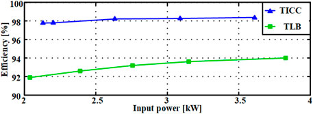
FIGURE 20. Measured efficiencies of the three-level boost converter and TICC converter under the same input voltage.
This paper proposes a three-input central capacitor converter for a high-voltage PV system, which can output a balanced three-level dc-link voltage and track the MPPs of three PV sources independently. The three-level structure enables it to be connected to the three-level inverter directly and reduces the voltage stress on semiconductors. Compared with the widely used boost and three-level boost converters, the proposed converter can reduce the mismatch losses and therefore has better energy harnessing ability due to the MPPT control of three split PV sources. Then, its operational principles and scalability are presented in detail. In addition, its corresponding control strategy is proposed to balance the three-level dc-link voltage when there is a large difference among the output power of three PV sources. A comparative study is carried out to demonstrate the advantages of the proposed converter, indicating its low semiconductor voltage/current stress and high efficiency. The performance of the three-input central capacitor converter along with its control strategy was verified by both simulation and experimental results.
The original contributions presented in the study are included in the article/Supplementary Material; further inquiries can be directed to the corresponding author.
XM and JL came up with the idea. XM is responible for carrying out the simulation and experiment verifications. GW and JF help check the simulation and experiment results.
Author JL was employed by State Grid Weihai Power Supply Company. GW was employed by State Grid Yantai Power Supply Company.
The remaining authors declare that the research was conducted in the absence of any commercial or financial relationships that could be construed as a potential conflict of interest.
All claims expressed in this article are solely those of the authors and do not necessarily represent those of their affiliated organizations or those of the publisher, the editors, and the reviewers. Any product that may be evaluated in this article or claim that may be made by its manufacturer is not guaranteed or endorsed by the publisher.
Abdullah, R., Rahim, N. A., Sheikh Raihan, S. R., and Ahmad, A. Z. (2014). Five-Level Diode-Clamped Inverter with Three-Level Boost Converter. IEEE Trans. Ind. Electron. 61, 5155–5163. doi:10.1109/TIE.2013.2297315
Agamy, M. S., Harfman-Todorovic, M., Elasser, A., Song Chi, S., Steigerwald, R. L., Sabate, J. A., et al. (2014). An Efficient Partial Power Processing DC/DC Converter for Distributed PV Architectures. IEEE Trans. Power Electron. 29, 674–686. doi:10.1109/TPEL.2013.2255315
Chen, M., Gao, F., Li, R., and Li, X. (2017). A Dual-Input Central Capacitor DC/DC Converter for Distributed Photovoltaic Architectures. IEEE Trans. Ind. Appl. 53, 305–318. doi:10.1109/TIA.2016.2606604
Choi, U.-M., Blaabjerg, F., and Lee, K.-B. (2015). Control Strategy of Two Capacitor Voltages for Separate MPPTs in Photovoltaic Systems Using Neutral-Point-Clamped Inverters. IEEE Trans. Ind. Appl. 51, 3295–3303. doi:10.1109/TIA.2015.2399611
Choudhury, A., Pillay, P., and Williamson, S. S. (2016). DC-bus Voltage Balancing Algorithm for Three-Level Neutral-Point-Clamped (NPC) Traction Inverter Drive with Modified Virtual Space Vector. IEEE Trans. Ind. Appl. 52, 3958–3967. doi:10.1109/TIA.2016.2566600
Dusmez, S., Hasanzadeh, A., and Khaligh, A. (2015). Comparative Analysis of Bidirectional Three-Level DC-DC Converter for Automotive Applications. IEEE Trans. Ind. Electron. 62, 3305–3315. doi:10.1109/TIE.2014.2336605
Elasser, A., Agamy, M., Sabate, J., Steigerwald, R., Fisher, R., and Harfman-Todorovic, M. (2010). A Comparative Study of Central and Distributed MPPT Architectures for Megawatt Utility and Large Scale Commercial Photovoltaic Plants. Proc. Ind. Electron. Conf., 2753–2758. doi:10.1109/IECON.2010.5675108
Gkoutioudi, E., Bakas, P., and Marinopoulos, A. (2013). Comparison of PV Systems with Maximum DC Voltage 1000V and 1500V. Proc. PVSC’ 2013, 2873–2878. doi:10.1109/PVSC.2013.6745070
Infineon (2017). Available at: https://www.infineon.com/dgdl/Infineon-FP10R12W1T4P-DS-v03.00CN.pdf?fileId=5546d46.25bd71aa0015bfbf6dcf2720b.
Jung-Min Kwon, J., Bong-Hwan Kwon, B., and Kwang-Hee Nam, K. (2008). Three-Phase Photovoltaic System with Three-Level Boosting MPPT Control. IEEE Trans. Power Electron. 23, 2319–2327. doi:10.1109/TPEL.2008.2001906
Karanayil, B., Ceballos, S., and Pou, J. (2019). Maximum Power Point Controller for Large-Scale Photovoltaic Power Plants Using Central Inverters under Partial Shading Conditions. IEEE Trans. Power Electron. 34, 3098–3109. doi:10.1109/TPEL.2018.2850374
Kim, J.-S., Kwon, J.-M., and Kwon, B.-H. (2018). High-Efficiency Two-Stage Three-Level Grid-Connected Photovoltaic Inverter. IEEE Trans. Ind. Electron. 65, 2368–2377. doi:10.1109/TIE.2017.2740835
Kjaer, S. B., Pedersen, J. K., and Blaabjerg, F. (2005). A Review of Single-phase Grid-Connected Inverters for Photovoltaic Modules. IEEE Trans. Ind. Appl. 41, 1292–1306. doi:10.1109/TIA.2005.853371
Kjaer, S. (2004). Aalborg East, Denmark: Inst. Energy Technol., Aalborg University. Ph.D. dissertation.Design and Control of an Inverter for Photovoltaic Applications
Liu, J., Gao, F., Chen, M., and Wang, G. (2018). “Communication-Less Control of Two-Stage Photovoltaic System with Multiple Distributed Dual-Input Central Capacitor Converters,” in 2018 IEEE Energy Conversion Congress and Exposition (ECCE), Portland, OR, USA. 23-27 Sept. 2018, 6392–6397. doi:10.1109/ECCE.2018.8557444
Lyu, J., Hu, W., Wu, F., Yao, K., and Wu, J. (2015). Variable Modulation Offset SPWM Control to Balance the Neutral-Point Voltage for Three-Level Inverters. IEEE Trans. Power Electron. 30, 7181–7192. doi:10.1109/TPEL.2015.2392106
Moghadasi, A., Sargolzaei, A., Anzalchi, A., Moghaddami, M., Khalilnejad, A., and Sarwat, A. (2018). A Model Predictive Power Control Approach for a Three-phase Single-Stage Grid-Tied PV Module-Integrated Converter. IEEE Trans. Ind. Appl. 54, 1823–1831. doi:10.1109/TIA.2017.2787626
Olalla, C., Deline, C., Clement, D., Levron, Y., Rodriguez, M., and Maksimovic, D. (2015). Performance of Power-Limited Differential Power Processing Architectures in Mismatched PV Systems. IEEE Trans. Power Electron. 30, 618–631. doi:10.1109/TPEL.2014.2312980
Park, Y., Sul, S.-K., Lim, C.-H., Kim, W.-C., and Lee, S.-H. (2013). Asymmetric Control of DC-Link Voltages for Separate MPPTs in Three-Level Inverters. IEEE Trans. Power Electron. 28, 2760–2769. doi:10.1109/TPEL.2012.2224139
Qian Zhang, Q., Changsheng Hu, C., Lin Chen, L., Amirahmadi, A., Kutkut, N., Shen, Z. J., et al. (2014). A Center Point Iteration MPPT Method with Application on the Frequency-Modulated LLC Microinverter. IEEE Trans. Power Electron. 29, 1262–1274. doi:10.1109/TPEL.2013.2262806
Rivera, S., Wu, B., Kouro, S., Yaramasu, V., and Wang, J. (2015). Electric Vehicle Charging Station Using a Neutral Point Clamped Converter with Bipolar DC Bus. IEEE Trans. Ind. Electron. 62, 1999–2009. doi:10.1109/TIE.2014.2348937
Serban, E., Ordonez, M., and Pondiche, C. (2015). DC-bus Voltage Range Extension in 1500 V Photovoltaic Inverters. IEEE J. Emerg. Sel. Top. Power Electron. 3, 901–917. doi:10.1109/JESTPE.2015.2445735
Shenoy, P. S., Kim, K. A., Johnson, B. B., and Krein, P. T. (2013). Differential Power Processing for Increased Energy Production and Reliability of Photovoltaic Systems. IEEE Trans. Power Electron. 28, 2968–2979. doi:10.1109/TPEL.2012.2211082
Stauth, J. T., Seeman, M. D., and Kesarwani, K. (2013). Resonant Switched-Capacitor Converters for Sub-module Distributed Photovoltaic Power Management. IEEE Trans. Power Electron. 28, 1189–1198. doi:10.1109/TPEL.2012.2206056
Tafti, H. D., Maswood, A. I., Konstantinou, G., Pou, J., and Blaabjerg, F. (2018). A General Constant Power Generation Algorithm for Photovoltaic Systems. IEEE Trans. Power Electron. 33, 4088–4101. doi:10.1109/TPEL.2017.2724544
Tan, F. D., and Middlebrook, R. D. (1995). A Unified Model for Current-Programmed Converters. IEEE Trans. Power Electron. 10, 397–408. doi:10.1109/63.391937
Tan, L., Wu, B., Yaramasu, V., Rivera, S., and Guo, X. (2016). Effective Voltage Balance Control for Bipolar-DC-Bus-Fed EV Charging Station with Three-Level DC-DC Fast Charger. IEEE Trans. Ind. Electron. 63, 4031–4041. doi:10.1109/TIE.2016.2539248
Tofoli, F. L., Pereira, D. d. C., Josias de Paula, W., and Oliveira Júnior, D. d. S. (2015). Survey on Non‐isolated High‐voltage Step‐up Dc-Dc Topologies Based on the Boost Converter. IET Power Electron. 8, 2044–2057. doi:10.1049/iet-pel.2014.0605
Vekic, M., Porobic, V., Grabic, S., Adzic, E., and Zogogianni, C. (2017). Explicit Active Power Reference Tracking Algorithm for Photovoltaic Converter. Proc. Ee’, 1–6. doi:10.1109/PEE.2017.8171707
Yan, C., Xu, D., and Chen, W. (2019). General Control Scheme for a Dual-Input Three-Level Inverter. IEEE Trans. Power Electron. 34, 1838–1850. doi:10.1109/TPEL.2018.2829903
Yaramasu, V., and Wu, B. (2014). Predictive Control of a Three-Level Boost Converter and an NPC Inverter for High-Power PMSG-Based Medium Voltage Wind Energy Conversion Systems. IEEE Trans. Power Electron. 29, 5308–5322. doi:10.1109/TPEL.2013.2292068
Keywords: PV system, three-level converter, central capacitor converter, photovoltaic (PV), dc-link voltage
Citation: Meng X, Liu J, Wang G and Fang J (2022) A Three-Input Central Capacitor Converter for a High-Voltage PV System. Front. Energy Res. 10:930471. doi: 10.3389/fenrg.2022.930471
Received: 28 April 2022; Accepted: 06 June 2022;
Published: 22 July 2022.
Edited by:
Savas Sonmezoglu, Karamanoğlu Mehmetbey University, TurkeyCopyright © 2022 Meng, Liu, Wang and Fang. This is an open-access article distributed under the terms of the Creative Commons Attribution License (CC BY). The use, distribution or reproduction in other forums is permitted, provided the original author(s) and the copyright owner(s) are credited and that the original publication in this journal is cited, in accordance with accepted academic practice. No use, distribution or reproduction is permitted which does not comply with these terms.
*Correspondence: Jiaxin Liu, c2R1X2xpdWppYXhpbkAxNjMuY29t
Disclaimer: All claims expressed in this article are solely those of the authors and do not necessarily represent those of their affiliated organizations, or those of the publisher, the editors and the reviewers. Any product that may be evaluated in this article or claim that may be made by its manufacturer is not guaranteed or endorsed by the publisher.
Research integrity at Frontiers
Learn more about the work of our research integrity team to safeguard the quality of each article we publish.