
95% of researchers rate our articles as excellent or good
Learn more about the work of our research integrity team to safeguard the quality of each article we publish.
Find out more
ORIGINAL RESEARCH article
Front. Energy Res. , 11 July 2022
Sec. Smart Grids
Volume 10 - 2022 | https://doi.org/10.3389/fenrg.2022.926707
This article is part of the Research Topic Power Quality and Electromagnetic Compatibility in Renewable Energy Systems View all 7 articles
DC voltage utilization and AC voltage harmonics are important evaluation indexes for Auxiliary Power Converter in Railway Applications. To improve the above two indicators, a novel switch-mode modulation method and quasi-PR control strategy for Buck-H three-phase inverter is proposed in this paper. The Buck-H three-phase inverter integrates the AC side filter circuit into the DC Buck circuit, which reduces the volume of the filter capacitor and improves the filtering effect. This novel switch-mode modulation method uses only one high frequency switch per phase, which reduces the switching losses and thereby increases overall efficiency. In addition, this switch-mode modulation absence of shoot-through menace eliminates the dead time requirement. Meanwhile, the quasi-proportional-resonance (PR) controller and its control parameters are optimized to improve the AC voltage tracking performance. The influence of PR control parameters on system performance is analyzed in detail. The proposed switch-mode modulation method and control method can effectively reduce the harmonic distortion rate of the system. The effectiveness is verified through the StarSim hardware-in-the-loop experimental results.
Auxiliary power converter is widely used in electrical fields such as power supplies, renewable energies, motor drives, and uninterruptible power supplies (Xu et al., 2016; Costa et al., 2018). Among various converter topologies, the three-phase inverter based on the three-phase bridge structure has been extensively studied for its simple structure, flexible control, and interconnection with the grid. DC voltage utilization and AC voltage harmonics are important evaluation indexes for three-phase bridge inverters. The DC voltage utilization is closely related to the efficiency of the inverter. Advances in the utilization of DC voltage can improve the load capacity of the inverter and reduce the voltage stress of the power device (Rahman et al., 2019). Additionally, for some high-end equipment such as auxiliary power supply of EMU, uninterruptible power supplies, aerospace power systems, and variable-speed AC machine drives, AC voltage with a lower harmonic distortion rate is necessary (Raymundo et al., 2017). However, the conventional three-phase bridge inverter and its modulation strategy are limited to improving the DC voltage utilization and reducing the harmonic distortion rate (Xiao et al., 2014; F. Jiang et al., 2021), which are essential performance evaluation indexes of inverters. Therefore, the conventional three-phase bridge inverters are not suitable for these particular applications, and a new topology structure or control strategy is urgently needed.
In (Shukla et al., 2018; Kalair et al., 2017), the sinusoidal pulse width modulation (SPWM) is used, and the maximum DC voltage utilization of the three-phase inverter is only 0.866. In (Pan et al., 2020), the space vector pulse width modulation method (SVPWM) is proposed to experiment the control of inverter. In (Li et al., 2019), the superiority of SVPWM in controlling inverters is then verified theoretically and experimentally. Compared with SPWM, utilization of DC voltage of SVPWM can be increased by 15.47% (Nallamekala et al., 2016; Choi et al., 2015). The bridge inverter based on PWM modulation has a theoretical maximum DC voltage utilization of 1, but the higher utilization is limited.
As for the harmonic distortion rate of AC voltage on the inverter’s output side, a multi-level converter topology is proposed in (Wang et al., 2015; Feng et al., 2019). The AC voltage levels in the multi-level inverter is more than or equal to three. The more the AC voltage levels, the closer the voltage wave to a sine wave and the fewer harmonics. However, as the voltage levels increase, the system structure and controller become more complicated, resulting in poor reliability and stability (Li et al., 2016). In addition (Karwatzki et al., 2018), propose the use of LCL filter to reduce the harmonics of inverter. Although LCL filter can eliminate some harmonics, it tends to cause resonance problems, which reduces the stability of the inverter (Gautam et al., 2017). Therefore, a simple three-phase inverter and its corresponding control method are highly desirable for a three-phase grid-connected system with high efficiency and reliability.
The purpose of this paper is to propose a novel switch-mode modulation method and quasi-PR control strategy for Buck-H three-phase inverter. The novel switch-mode modulation method integrates the AC side filter circuit into the Buck circuit, so that the AC output side does not need passive filter components such as inductors and capacitors. Compared with the traditional inverter filter capacitor, the DC filter capacitor in this topology is smaller and has a better filtering effect.
1) Compared with the conventional inverter filter capacitor, the DC filter capacitor in the novel Buck-H three-phase inverter topology is smaller and has a better filtering effect.
2) The H-bridge in the inverter topology is designed to be controlled synchronously with the power frequency of 50 Hz to solve the shoot through problem and reduce reverse recovery lose. This design method effectively reduces the harmonic distortion rate of the AC voltage.
3) A quasi-PR control method and its control parameters are designed to improve the inverter’s DC voltage utilization.
The rest of this paper is organized as follows. In Topology and Working Principle, the novel switch-mode modulation method for the Buck-H three-phase inverter is presented. The working principle and switching method for the Buck-H inverter are introduced in detail. In Control Strategy and Parameter Design, a quasi-PR control method for the Buck-H three-phase inverter is proposed. Simulation results are shown in Simulation Analysis and Experimental results are provided in Experimental Verification. Finally, Conclusion concludes this paper.
This paper takes the three-phase auxiliary inverter in the traction drive system of CRH5 EMU as the research object, as shown in Figure 1. Among them, the three-phase inverter converts the front DC into 380 V AC for the normal operation of auxiliary equipment in the carriage (such as air conditioning, lighting, etc.). However, the traditional three-phase inverter topology is usually composed of H-bridge circuit, which is difficult to provide high-quality power quality. This paper proposes a novel switch-mode modulation method for Buck-H three-phase inverter is shown in Figure 2;
The front end of each phase of the inverter is a Buck converter, as shown in Figure 3 its steady-state output voltage is:
Where
Assuming the DC voltage is constant, the duty cycle α will change regularly with the inverting fully rectified sinusoidal (as shown in Figure 4A) by controlling the switching frequency change:
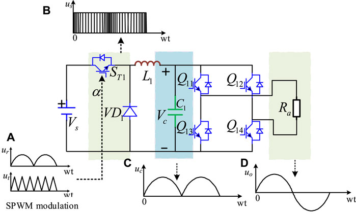
FIGURE 4. Schematic diagram of main principle waveforms: (A) waveform of modulated signal, (B) output equivalent sine half-wave waveform, (C) steady-state output voltage waveform, (D) output voltage waveform of inverter.
Therefore, the output voltage at the output end of the power switch ST1 is an equivalent sine half-wave PWM as shown in Figure 4B.
Then through the LC filter in the Buck circuit, only the sinusoidal positive half-cycle DC pulsation waveform is output as shown in Figure 4C. The following H bridge is synchronized with the power frequency of 50 Hz, so there is no reverse recovery lose and the shoot through problem. The inverting fully rectified sinusoidal is transformed into a standard sine wave through the alternate conduction of Q11/Q14 and Q12/Q13 as shown in Figure 4D.
However, in a conventional H bridge inverter, the dead time is necessary to prevent the short circuit and damage caused by the simultaneous conduction of the switches. It is set between the driving signals of two switches in the same branch. Nevertheless, the introduction of the dead time will increase the harmonic voltage.
Although there are many switches for the Buck-H three-phase inverter using the switching mode proposed in this paper, only ST1, ST2, and ST3 power switches work at high frequency. The other switches in the H-bridge circuit are zero voltage switching and zero current switching, namely soft switching. And little or no loss is produced in this switch state. The switching loss of the inverter mainly comes from high-frequency switches. The high-frequency switches in the Buck-H three-phase inverter are half less than the conventional three-phase H bridge inverter, which dramatically reduces the switching loss. Furthermore, the utilization of DC voltage is improved to a certain extent.
If the PWM waveforms of ST1, ST2 and ST3 change with the inverting fully rectified sine wave and have a phase difference of 120°, it can be seen from Eq. 2 that the duty ratios of the power switch ST1, ST2 and ST3 in Figure 1 also follow the inverting fully rectified sine wave with a phase difference of 120°. So the duty ratios of ST1, ST2, and ST3 in the three-phase inverter are:
Where m is the modulation factor, its expression is:
Combining Formula (3), Eq. 5 can be obtained:
It can be seen from the above formulas that the voltages
The four switches of each phase in the H-bridge operate at a certain frequency (50 Hz) and work in a soft-switching state. Therefore, there is almost no loss in this switching state, thus improving the efficiency of the whole system to a certain extent. The voltage in Eq. 6 is the phase voltage with a phase difference of 120°, and the maximum phase voltage peak value is Vs. As the three phases are symmetric, the line voltage can be deduced from Eq. 6 as follows:
Therefore, when the modulation ratio is 1, the maximum line voltage peak value can be obtained as
Where
So the maximum DC voltage utilization of the Buck-H inverter is √3≈1.73. However, when SPWM is used in the traditional H bridge three-phase inverter, the maximum DC voltage utilization is only 0.866. Even with SVPWM modulation or third harmonic injection, the maximum DC voltage utilization can be achieved only 1 (Arshadi et al., 2016). Therefore, the Buck-H three-phase inverter using the switching mode proposed in this paper has a significant advantage over the traditional H bridge three-phase inverter in DC voltage utilization.
There are four switching modes for each phase of five power switches. Taking A-phase as an example, the current loop and equivalent circuit in each switching mode are shown in Figure 5 respectively.
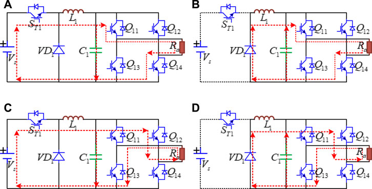
FIGURE 5. Equivalent circuit diagram of each switching mode: (A) ST1 is on, Q11 and Q14 are on, and Q12 and Q13 are off, (B) ST1 is off, Q11 and Q14 are on, and Q12 and Q13 are off, (C) ST1 is on, Q11 and Q14 are off, and Q12 and Q13 are on, (D) ST1 is off, Q11 and Q14 are off, and Q12 and Q13 are on.
In mode 1 (as shown in Figure 5A): ST1 is on, Q11 and Q14 are on, Q12 and Q13 are off. At this point, current flows through VS, ST1, L1, Ra, Q11 and Q14 to form a circuit, while the DC power supply charges capacitor C1 to supply power to the load.
In mode 2 (as shown in Figure 5B): ST1 is off, Q11 and Q14 are on, and Q12 and Q13 are off. At this point, current flows through VD1, L1, Ra, Q11 and Q14 to form a circuit. Meanwhile capacitor C1 is discharged, and VD1 plays the role of free-wheeling.
In mode 3 (as shown in Figure 5C): ST1 is on, Q11 and Q14 are off, and Q12 and Q13 are on. The current forms a loop through Vs, ST1, Ra, Q14, and Q13. At the same time, the DC power supply charges capacitor and supply power to the load.
In mode 4 (as shown in Figure 5D): ST1 is off, Q11 and Q14 are off, and Q12 and Q13 are on. At this time, the current forms a loop through VD1, L1, Q14, Ra and Q13, the capacitor C1 discharged, and VD1 continues to flow.
The H-bridge following the Buck converter consists of four switches (Q11-Q14). H-bridge is used to realize the function of synchronous inverting with reference voltage, as shown in Figure 6.
At 0 ∼ T/2 and T ∼ 3/2T, the switch Q11 and Q14 are on while the switch Q12 and Q13 are off; at T/2∼T and 3/2∼2T, the switch Q12 and Q13 are on, while the switch Q11 and Q14 are off. Therefore, the capacitor voltage Vc at the output side is turned into the standard sinusoidal output voltage Voa.
The traditional PI controller is composed of proportional and integral links. Its transfer function is:
Its gain at the fundamental frequency
It can be seen from Eqs 9, 10 that the PI controller is a linear controller. The gain at the fundamental frequency is a limited value. So it can only track the DC value accurately. If PI control is to be used in three-phase AC system, complex coordinate transformation of abc/dq or αβ/dq must be carried out to change AC into DC to realize static error free tracking control.
To overcome the defects of the PI controller, the PR controller is proposed in (Parvez et al., 2020; Alemi et al., 2016). The transfer function is:
The root locus analysis shows that the PR controller is compared with the PI controller. The transfer function adds two closed-loop poles of fixed frequency on the imaginary axis of the s-plane to form resonance. So it can realize static error-free tracking control of AC at this frequency (Pan., 2018). Compared with the PI controller, the gain of the PR controller at a certain frequency is infinite. As a result, it can realize static error-free tracking control of AC at a specific frequency. In the control design of the current inner loop, there is no need for complex dq coordinate transformation and coupling relation between dq axes. Hence the control system design is simplified. However, in the actual power grid, the bandwidth of the ideal PR controller is narrow due to the frequency fluctuation of the power grid. Therefore, it cannot adapt to the actual power grid fluctuation. A quasi-PR controller is proposed to solve this problem. Its transfer function is:
Compared with the PR controller, a zero point in the transfer function of the PR controller is added to the quasi-PR controller, which increases the bandwidth of the controller and adapts to the power grid with actual frequency fluctuation. Hence the problem of poor control performance caused by frequency fluctuation is solved effectively.
It can be seen from Eq. 13 that the transfer function of quasi-PR controller contains three variables
1) Set
It can be seen from the above figure that as the kr parameter increases, the gain of the controller also increases, while the bandwidth of the control does not change. Therefore, the kr parameter only affects the gain of the controller, not the bandwidth. The gain of the controller is proportional to kr. The larger kr is, the larger the gain is and the smaller the steady-state error is. However, if kr is too large, the harmonic component will be amplified, thus reducing the quality of the grid-connected current. Therefore, when selecting kr, it is necessary to ensure that the system has sufficient gain near the fundamental frequency, and there should be a certain attenuation effect away from the fundamental frequency.
2) Set kp = 1,
It can be seen from Figure 7 that the gain and bandwidth of the controller increase with
3) Set
It can be seen from Figure 8 that the
Therefore, in engineering application, the design steps of quasi-PR controller parameters are as follows: Determine the controller bandwidth according to the allowable fluctuation range of frequency, and then select
This section simplifies the overall control strategy using phase A as an example. The control strategy of each phase is shown in Figure 10. The other phases B and C are similar except that the phase difference of the reference signal is given at 120°.
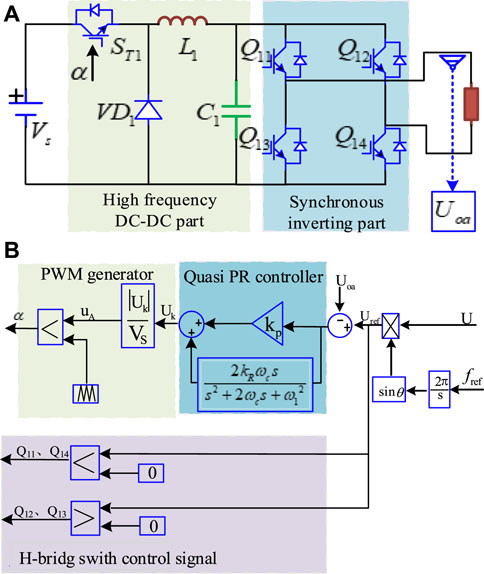
FIGURE 10. Control strategy of Buck-H three-phase inverter(A) A phase main circuit structure, (B) A phase switch control strategy.
To enable the three-phase inverter output voltage amplitude constant and frequency when the inverter AC load fluctuates, a closed-loop control strategy is used (as shown in Figure 10B). Firstly, the phase angle
Then the output AC voltage
Through PWM modulation, the control signal of high frequency switch ST1 of Buck converter is obtained. H-bridge circuit is used to realize the synchronous reversal of DC pulse voltage wave at the output of Buck converter in 50 Hz. Therefore, the control signal generation method of the four switches of each phase H-bridge is shown in Figure 10B. The reference voltage Uref of 50 Hz is compared with 0 respectively. When the reference voltage is greater than 0, the switches Q11 and Q14 are on, while the switches Q12 and Q13 are off. So the output voltage is positive half-cycle waveform of sinusoidal voltage. When the reference voltage is less than 0, Q12, Q13 are on, Q11, Q14 are off. Hence the output voltage is a negative half-cycle waveform of a sine wave voltage.
The simulation model of the Buck-H three-phase inverter was built in MATLAB/Simulink. The simulation parameters are as follows (take phase A as an example): DC power supply voltage is 311 V. The effective values of inverter output phase voltage and line voltage are 220 and 380 V with 50 Hz respectively. The load resistance is 20Ω, and the inductance of Buck circuit is 6 mH. The capacitance is 10uF, and the switching frequency is 10 kHz. The parameters of the quasi-PR controller are
Figure 11 shows the A-phase voltage and current waveforms of the Buck-H three-phase inverter under PI control and Quasi PR control respectively. It can be seen from Figure 11A that the output voltage of the inverter is a standard 50 Hz AC. The output voltage peak value is stabilized at 311 V after 0.01 s, thus realizing constant voltage and frequency control. However, the system output voltage and current waveform fluctuates at the over-zero point under PI control, and smooth switching cannot be achieved. Secondly, the amplitude of the output voltage is only 305 V and the current size is only 12 A.
In the simulation, the load is suddenly doubled at 0.2 s to verify that the inverter can still achieve constant voltage and frequency output. The dynamic process of its output phase voltage and current is shown in Figure 12.
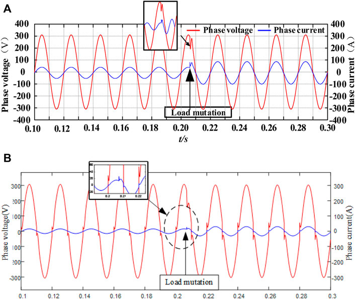
FIGURE 12. Waveforms of A-phase voltage and phase current during load mutation (A) with Quasi PR control, (B) with PI control.
Figure 12 shows the dynamic waveforms of output voltage and current by the Buck-H three-phase inverter when the load is changed suddenly under PI control and Quasi PR control respectively. As shown in Figure 12A, the peak value of the output phase current increases from 15.5 to 31 A when the load suddenly doubles in 0.2 s, namely, the output power is also doubled. When the load suddenly doubled, the output three-phase phase voltage of the inverter fluctuated at 0.2 s, from a peak value of 311–330 V. However, the 50 Hz AC steady-state output of peak value of 311 V is restored shortly after 0.22 s. In this way, a steady-state output of constant voltage and frequency can be realized in the case of load mutation. However, under the same operating conditions, the output voltage and current waveforms under PI control cannot be smoothly transitioned at the over-zero point, and the overall effect is worse than that of quasi-PR control.
Figure 13 shows the output three-phase voltage waveform of three-phase inverters in different modes. It can be seen from Figure 13 that the peak value of line voltage in Buck-H three-phase inverter is about 538 V. However, when the DC power supply is 311 V, and traditional three-phase inverter is modulated with SPWM. The maximum peak value of output line voltage is:
Even if the SVPWM modulation or third harmonic injection method is adopted, the maximum peak value of output line voltage in a three-phase inverter is only 311 V. Therefore, compared with the conventional three-phase inverter with SPWM, the DC voltage utilization of this Buck-H three-phase inverter is improved by two times. Similarly, the DC voltage utilization is 1.73 times higher than the SVPWM.
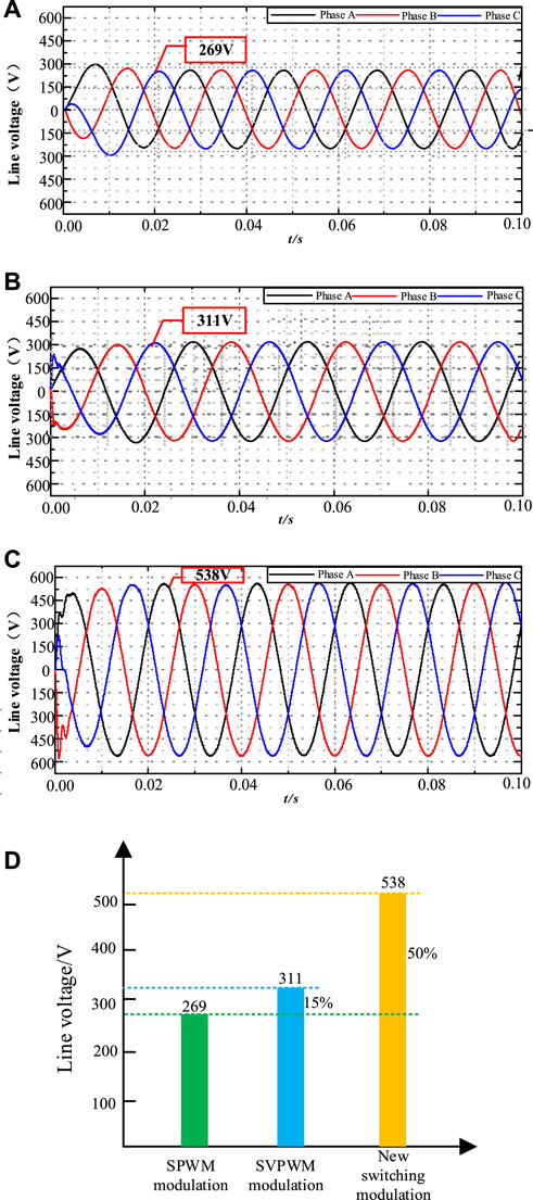
FIGURE 13. Three-phase voltage output by inverters in different modes:(A) Output line voltage of three phase bridge inverter modulated by SPWM, (B) Output line voltage of three phase bridge inverter modulated by SVPWM, (C) Output line voltage of Buck-H three phase inverter, (D) Comparison of output line voltage of three phase inverter with different switching modes.
With the same filter inductance and capacitance, the harmonic content of output current in the conventional three-phase H-bridge inverter and Buck-H three-phase inverter is compared, as shown in Figure 14.
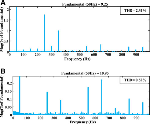
FIGURE 14. Comparison of harmonic content of inverter output current:(A) output phase voltage spectrum of traditional three phase bridge inverter controlled by SPWM, (B) output phase voltage spectrum of Buck-H three phase inverter with quasi-PR control.
It can be seen from Figure 14A that the total harmonic distortion (THD) of the output current in a conventional three-phase H-bridge inverter is 2.31%. However, the THD of the Buck-H three-phase inverter proposed in this paper is only 0.52%, and the maximum single harmonic content is less than 0.3%. The results show that the Buck-H three-phase inverter can significantly reduce the harmonic content compared to the conventional H-bridge three-phase inverter. The simulation results are consistent with the conclusions drawn from the above operating principle analysis.
To further verify the correctness of the topology and control strategy proposed in this paper, the hardware in the loop simulation platform of the Buck-H three-phase inverter system is built shown in Figure 2. The primary circuit model is built in Simulink software, and the host computer StarSim HIL software of Modeling Tech is used to make the primary circuit run on the FPGA board in the StarSim MT6016 chassis. The controller adopts TMS320F28335 of the C2000 series of TI company. The host computer and the controller realize signal interaction through the interface box to form a closed-loop system.
Among them, the control circuit is completed by DSP, and the hardware circuit is completed on the hardware in the loop (HIL) real-time simulation platform. The limit interval value of the analog output/input of the main circuit in StarSim HIL real-time simulator is (-10,10) V, and the limit interval of the digital output/input of the DSP controller is (0,3.3) V. The main circuit topology is consistent with Figure 1, and the main parameters of the experimental platform are shown in Table 1. Since the voltage ranges of I/O ports of HIL is [- 10,10] V, it is necessary to multiply the electrical quantity to be measured by the corresponding proportional coefficient before output and detect it by oscilloscope. The experimental platform is shown in Figure 15.
Three symmetric load and asymmetric load with a resistance value of 20Ω are connected for comparative experimental to verify the overall performance of the proposed Buck-H three-phase inverter. According to the experimental waveform as shown in Figures 16, 17, it can be seen that the output voltage of the Buck-H inverter is the standard 50Hz AC, and the peak output voltage is stable at 311 V. Then double the A-phase load, as can be seen from Figure 16, when the A-phase load suddenly doubles, the peak value of the output A-phase current increases from 15.5 to 31 A, so the output power also doubles. When the A-phase load is doubled suddenly, the output three-phase voltage of the inverter fluctuates at the moment of sudden change, but the 50 Hz AC steady-state output with a peak value of 311 V is quickly restored.
The comparison experiment between SPWM modulation and SVPWM modulation was conducted on the experimental platform to verify the correctness and effectiveness of the proposed control strategy. The experimental waveforms are shown in Figures 18–20.
According to the experimental waveforms, it can be seen that the output line voltage peak of the Buck-H three-phase inverter using the proposed control strategy is about 538 V. When the DC power supply is 311 V, and the SPWM modulation is adopted for the conventional three-phase inverter, the maximum output line voltage peak value is 269 V. Even if the SVPWM modulation method or three harmonic injection methods are introduced, the maximum output line voltage is only 311 V. Therefore, the Buck-H three-phase inverter using the switching mode proposed in this paper significantly improves the utilization of DC voltage compared with the conventional three-phase inverter.
In this paper, a novel switch-mode modulation method and quasi-PR control strategy for Buck-H three-phase inverter is proposed. The novel switch-mode modulation method for Buck-H three-phase inverter is introduced, along with the working principle and switching mode. The quasi-PR control is constructed for the Buck-H topology, which can improve the system’s dynamic performance. The following conclusions can be drawn from the theoretical and experimental results.
1) Compared with the conventional SPWM and SPVWM in the H-bridge inverter, the DC voltage utilization in the novel Buck-H three-phase inverter is improved by 2 times and 1.73 times, which significantly enhances the load-carrying capacity of the inverter.
2) The novel switch-mode modulation method for Buck-H three-phase inverter has a lower harmonic distortion rate. By integrating the AC side filter circuit into the Buck circuit, reducing the introduction of harmonics to a certain extent.
3) The novel switch-mode modulation method can reduce the system volume and cost. The capacitor voltage in the Buck circuit is DC. Compared with the conventional inverter, the DC filter capacitor in this paper has a smaller volume and better filtering effect.
The original contributions presented in the study are included in the article/supplementary material, further inquiries can be directed to the corresponding author.
Conceptualization, ZL and FW; methodology, ZL, FW, and JZ; software, ZL and FW; validation, ZL, FW, JZ, and DH; formal analysis, ZL, FW, JZ, and DH; investigation, ZL, FW, JZ, and DH; resources, ZL; data curation, FW; writing—original draft preparation, ZL, FW, and DH; writing—review and editing, ZL, FW, and JZ; visualization, XY and FX; supervision, JZ and FX; funding acquisition, ZL. All authors have read and agreed to the published version of the manuscript.
This work was supported in part by the National Natural Science Foundation of China under Grant 51807058, by the Natural Science Foundation of Hunan Province under Grant 2020JJ6082, 2021JJ50002 and in part by Scientific research and Scientific research and innovation Foundation of Hunan University of Technology under Grant CX2111.
The authors declare that the research was conducted in the absence of any commercial or financial relationships that could be construed as a potential conflict of interest.
All claims expressed in this article are solely those of the authors and do not necessarily represent those of their affiliated organizations, or those of the publisher, the editors and the reviewers. Any product that may be evaluated in this article, or claim that may be made by its manufacturer, is not guaranteed or endorsed by the publisher.
Alemi, P., Bae, C.-J., and Lee, D.-C. (2016). Resonance Suppression Based on PR Control for Single-phase Grid-Connected Inverters with Filters. IEEE J. Emerg. Sel. Top. Power Electron. 4 (2), 459–467. June 2016. doi:10.1109/jestpe.2015.2464699
Arshadi, S. A., Poorali, B., Adib, E., and Farzanehfard, H. (2016). High Step-Up DC-AC Inverter Suitable for AC Module Applications. IEEE Trans. Ind. Electron. 63 (2), 832–839. Feb. 2016. doi:10.1109/tie.2015.2480387
Choi, J.-H., Kim, S., Yoo, D. S., and Kim, K.-H. (2015). A Diagnostic Method of Simultaneous Open-Switch Faults in Inverter-Fed Linear Induction Motor Drive for Reliability Enhancement. IEEE Trans. Ind. Electron. 62 (7), 4065–4077. Jul. 2015. doi:10.1109/tie.2014.2385044
de Azevedo Cavalcanti Costa, L. A. L., Vitorino, M. A., and de Rossiter Correa, M. B. (2018). Improved Single-phase AC-DC-AC Current Source Converter with Reduced DC-Link Oscillation. IEEE Trans. Ind. Appl. 54 (3), 2506–2516. May-Jun. 2018. doi:10.1109/tia.2018.2799186
Jiang, F., Peng, X., Tu, C., Guo, Q., Deng, J., and Dai, F. (2021). An Improved Hybrid Parallel Compensator for Enhancing PV Power Transfer Capability. IEEE Trans. Ind. Electron. doi:10.1109/TIE.2021.3121694
Feng, J., Li, Q., Lee, F. C., and Fu, M. (2019). Transmitter Coils Design for Free-Positioning Omnidirectional Wireless Power Transfer System. IEEE Trans. Ind. Inf. 15 (8), 4656–4664. Aug. 2019. doi:10.1109/tii.2019.2908217
Gautam, S. P., Kumar, L., Gupta, S., and Agrawal, N. (2017). A Single-phase Five-Level Inverter Topology with Switch Fault-Tolerance Capabilities. IEEE Trans. Ind. Electron. 64 (3), 2004–2014. March 2017. doi:10.1109/tie.2016.2626368
Kalair, A., Abas, N., Kalair, A. R., Saleem, Z., and Khan, N. (2017). Review of Harmonic Analysis, Modeling and Mitigation Techniques. Renew. Sustain. Energy Rev. 78 (April), 1152–1187. doi:10.1016/j.rser.2017.04.121
Karwatzki, D., and Mertens, A. (2018). Generalized Control Approach for a Class of Modular Multilevel Converter Topologies. IEEE Trans. Power Electron. 33 (4), 2888–2900. April 2018. doi:10.1109/tpel.2017.2703917
Lei, J., Zhou, B., Wei, J., Bian, J., Zhu, Y., Yu, J., et al. (2016). Predictive Power Control of Matrix Converter with Active Damping Function. IEEE Trans. Ind. Electron. 63 (7), 4550–4559. July 2016. doi:10.1109/tie.2016.2541599
Li, D., Chen, Q., and Zhang, C. (2016). A High-Power Active Filtering System with Fundamental Magnetic Flux Compensation. Power Deliv. IEEE Trans. 21 (2), 823–830. doi:10.1109/TPWRD.2006.871009
Li, Y., Yang, X., Chen, W., Liu, T., and Zhang, F. (2019). Neutral-Point Voltage Analysis and Suppression for NPC Three-Level Photovoltaic Converter in LVRT Operation under Imbalanced Grid Faults with Selective Hybrid SVPWM Strategy. IEEE Trans. Power Electron. 34 (2), 1334–1355. Feb. 2019. doi:10.1109/tpel.2018.2834226
Nallamekala, K. K., and Sivakumar, K. (2016). A Fault-Tolerant Dual Three-Level Inverter Configuration for Multipole Induction Motor Drive with Reduced Torque Ripple. IEEE Trans. Ind. Electron. 63 (3), 1450–1457. March 2016. doi:10.1109/tie.2015.2495281
Pan, Y., and Li, Y. (2020). Fuzzy Filter Design in Finite-Frequency Domain for Three-Level Inverter Drive System. IEEE Access 8, 3792–3801. doi:10.1109/access.2019.2962105
Pan, Z., Dong, F., Zhao, J., Wang, L., Wang, H., and Feng, Y. (2018). Combined Resonant Controller and Two-Degree-Of-Freedom PID Controller for PMSLM Current Harmonics Suppression. IEEE Trans. Ind. Electron. 65 (9), 7558–7568. Sept. 2018. doi:10.1109/tie.2018.2793232
Parvez, M., Elias, M. F. M., Rahim, N. A., Blaabjerg, F., Abbott, D., and Al-Sarawi, S. F. (2020). Comparative Study of Discrete PI and PR Controls for Single-phase UPS Inverter. IEEE Access 8, 45584–45595. doi:10.1109/access.2020.2964603
Rahman, K., Iqbal, A., Al-Hitmi, M. A., Dordevic, O., and Ahmad, S. (2019). Performance Analysis of a Three-To-Five Phase Dual Matrix Converter Based on Space Vector Pulse Width Modulation. IEEE Access 7, 12307–12318. doi:10.1109/access.2019.2892514
Raymundo, E., Olguin, T., and Garces, A. (2017). “Grid Integration of Offshore Wind Farms Using a Hybrid HVDC Composed by an MMC with an LCC-Based Transmission System,” in Energy Procedia. 137. 391–400. doi:10.1016/j.egypro.2017.10.363
Shukla, K., Malyala, V., and Maheshwari, R. (2018). A Novel Carrier-Based Hybrid PWM Technique for Minimization of Line Current Ripple in Two Parallel Interleaved Two-Level VSIs. IEEE Trans. Ind. Electron. 65 (3), 1908–1918. March 2018. doi:10.1109/tie.2017.2745438
Wang, K., Zhu, Z. Q., Ren, Y., and Ombach, G. (2015). Torque Improvement of Dual Three-phase Permanent-Magnet Machine with Third-Harmonic Current Injection. IEEE Trans. Ind. Electron. 62 (11), 6833–6844. Nov. 2015. doi:10.1109/tie.2015.2442519
Xiao, H., Liu, X., and Lan, K. (2014). Optimised Full-Bridge Transformerless Photovoltaic Grid-Connected Inverter with Low Conduction Loss and Low Leakage Current. IET Power Electron. 7 (4), 1008–1015. doi:10.1049/iet-pel.2013.0404
Keywords: three-phase inverter, soft switch, quasi-PR controller, DC voltage utilization, harmonic
Citation: Lan Z, Wu F, He D, Yu X, Zeng J and Xiao F (2022) A High Power Quality Buck-H Auxiliary Power Converter in Railway Applications. Front. Energy Res. 10:926707. doi: 10.3389/fenrg.2022.926707
Received: 23 April 2022; Accepted: 20 June 2022;
Published: 11 July 2022.
Edited by:
Fei Jiang, Changsha University of Science and Technology, ChinaReviewed by:
Renyou Xie, University of New South Wales, AustraliaCopyright © 2022 Lan, Wu, He, Yu, Zeng and Xiao. This is an open-access article distributed under the terms of the Creative Commons Attribution License (CC BY). The use, distribution or reproduction in other forums is permitted, provided the original author(s) and the copyright owner(s) are credited and that the original publication in this journal is cited, in accordance with accepted academic practice. No use, distribution or reproduction is permitted which does not comply with these terms.
*Correspondence: Dong He, aGQ4NjExMTZAMTYzLmNvbQ==
Disclaimer: All claims expressed in this article are solely those of the authors and do not necessarily represent those of their affiliated organizations, or those of the publisher, the editors and the reviewers. Any product that may be evaluated in this article or claim that may be made by its manufacturer is not guaranteed or endorsed by the publisher.
Research integrity at Frontiers

Learn more about the work of our research integrity team to safeguard the quality of each article we publish.