 Daniel Wei Zhang
 Jingyang Fang
 Stefan Goetz1
- 1Department of Electrical and Computer Engineering, Pratt School of Engineering, Duke University, Durham, NC, United States
- 2School of Control Science and Engineering, Shandong University, Jinan, China
The growth of renewable energies, together with their power converter interfaces, reshapes power systems into more-electronics power systems. Along with this paradigm shift is the requirement of grid formation by grid-tied power converters. However, existing grid architectures only allow parallel operation of grid-forming converters, which excludes high-voltage applications. This article proposes novel lattice power grids that combine the advantages of multilevel converters and power grids, thereby allowing both serial and parallel connectivity with modularity and scalability. Further, we propose control and optimization algorithms for lattice power grids by use of graph theory. In particular, we investigate H-bridge-based lattice power grids and achieve several objectives, including desired voltages and currents between any two selective nodes in lattice power grids as well as efficiency optimization by minimizing switching actions. To achieve these objectives, this article details control and optimization methodology for square lattice power grids. Finally, the proposed algorithms and lattice power grids are validated via simulation results.
1 Introduction
The desire to reduce carbon emissions and to meet the rising global energy demand has led to the drastic increase in penetration of renewable energy sources (U.S. Department of Energy Office of Energy Efficiency and Renewable Energy, 2018; Chappell, 2021). Unlike traditional power sources which interface with power grids through synchronous generators (Hooshyar and Vahedi, 2007), renewable sources such as photovoltaics and wind turbines are usually decentralized geographically and interface with power grids through grid-tied power converters (Fang et al., 2017; Fang et al., 2019; Fang, 2021a). Power systems primarily based on grid-tied power converters are known as more-electronics power systems (see Figure 1) (Fang et al., 2019; Fang, 2021a).
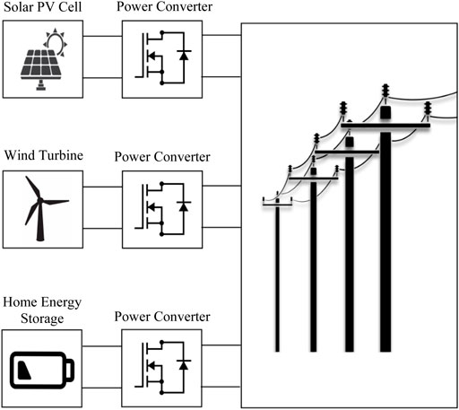
FIGURE 1. Schematic of more-electronics power system.
In conventional power systems, stability is guaranteed through the voltage/frequency support and rotational masses of synchronous generators, and grid-tied converters simply follow the established grid. However, the growing penetration of grid-tied power converters will necessitate grid-forming capabilities (Han et al., 2019; Deng et al., 2021; Lin, 2020; Fang, 2021a). As for current grid architectures, existing grid-forming converters can only be connected in parallel for current sharing, but they cannot withstand high voltages (Lin, 2020).
To undertake high voltages, multiple power electronic switches are connected in series to form multilevel converters (Das, 2019a; Fang et al., 2021a; Fang et al., 2021b). Among multilevel converters, cascaded-bridge converters (CBC), which consist of identical submodules in series, and modular multilevel converters (MMC), which replace individual active switches of two-level converters with CBC (Das, 2019a; Fang et al., 2021a; Fang et al., 2021b), stand out due to their modularity and scalability. Recently, research interests on multilevel converters with parallel connectivity in addition to serial connectivity have grown (Goetz et al., 2017; Fang et al., 2021b). Potential benefits of parallel connectivity include current sharing, reduced conduction losses, and sensorless voltage balancing. However, multilevel converters with parallel connectivity essentially connect a string of submodules (which tie each of their neighboring submodule with two terminals) in series. From a macroscopic point of view, such multilevel converters still feature a serial structure, thereby suffering from limited current ratings (Fang et al., 2021b).
Combining the parallel architecture of power systems and the serial structure of multilevel converters, this article proposes novel lattice power grids. A lattice power grid consists of multiple grid-forming converters arranged in a lattice structure. It shares the same topologies as the lattice converter, which is a newly developed power converter that aims to tile the two-dimensional plane or the three-dimensional space (Fang, 2021b; Fang and Goetz, 2021; Mei et al., 2022). The benefits of lattice power grids include the applicability to high-voltage and large-current applications, multiple input/output ports, as well as modularity and scalability (Fang and Goetz, 2021). The power converter efficiencies of lattice converters have been investigated by Mei et al. through simulations of lattice converters with 10 Ω load resistances and 0.01 Ω internal resistances. It was found that 3 × 3 and 4 × 4 lattice converters can achieve power converter efficiencies of 99.85 and 99.81%, respectively, and we seek to extend these benefits to lattice power grids. This article addresses the fundamental challenges of lattice power grids by use of graph theory.
The remainder of this article is organized as follows. Fundamentals of Lattice Power Grids section introduces the fundamentals of lattice power grids and introduces a method of modeling lattice power grids using graph theory. Objectives of the Proposed Control and Optimization Algorithms and Components of Control and Optimization Algorithms for Square Lattice Grids sections detail the algorithms that achieve desired voltage and current objectives for square lattice power grids. Generalizing the Proposed Algorithms for Various Lattice Structures section generalizes the proposed algorithms to other lattice types. Simulations and Results section provides simulation results for the proposed algorithms. Finally, concluding remarks are given in Conclusion section.
2 Fundamentals of Lattice Power Grids
2.1 Grid-Forming Converters and Multilevel Converters
A more-electronics power system consists primarily of generators and loads that interface with the power grid through individual power converters (Fang, 2021a; Fang et al., 2017; Fang et al., 2019). These power converters feature many different topologies, among which single-phase and three-phase bridges are popular, such as the H-bridge converter shown in Figure 2 (Das, 2019a; Fang et al., 2021b). This article is applicable to various grid-forming converters. As one example, we will focus primarily on single-phase H-bridge grid-forming converters.
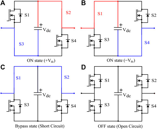
FIGURE 2. H-bridge converter states. (A) ON state (+Vdc). (B) ON state (−Vdc). (C) Bypass state (Short Circuit). (D) OFF state (Open Circuit).
The H-bridge converter is power electronic equipment that consists of a DC voltage source Vdc, four semiconductor switches, and passive filters. As the proposed lattice power grids allow the removal of passive filters, we illustrate the operation of H-bridge converters via Figure 2 (Das, 2019b). As seen, an H-bridge converter can take on one of the four states:
1) The H-bridge outputs a positive voltage.
2) The H-bridge outputs a negative voltage.
3) The H-bridge is in bypass mode, acting as a short circuit.
4) The H-bridge acts as an open circuit.
Existing grid architectures for more-electronics power systems do not allow high-voltage applications of grid-forming converters, only allowing for current sharing through parallel operation (Lin, 2020). To allow for high-voltage DC and AC applications, we can turn to the benefits of multilevel converters.
In recent decades, multilevel converters have emerged as a technology of substantial interests due to their wide-ranging applications. Common multilevel converters include CBC and MMC (Das, 2019a; Fang et al., 2021a; Fang et al., 2021b). Such power converters often consist of half-bridge or H-bridge submodules in serial connection to allow for the creation and transmission of high voltages using lower-voltage components. As a result, multilevel converters have found a wide variety of applications across the field of power electronics (Fang et al., 2021b; Flourentzou et al., 2009). The concept of multilevel converters can be expanded to more-electronics power systems as well, with each grid-tied power source (solar PV, wind turbine, etc.) representing a submodule in a power grid (Fang et al., 2017; Fang et al., 2019; Fang, 2021a).
A drawback of existing multilevel converters is that serial connection does not allow for current sharing, thus limiting current ratings. Recent research has investigated the potential of multilevel converters that allow for parallel connectivity (Goetz et al., 2015; Goetz et al., 2017; Das, 2019a; Fang et al., 2021a; Fang et al., 2021b). Connecting CBC branches in parallel allows for a greater amount of current to be delivered and the use of components with lower current ratings (Fang et al., 2021b).
2.2 Square Lattice Power Grids and Their Graph Model
The square lattice power grid consists of several grid-forming H-bridge converters connected in a lattice structure (see Figure 3A). Lattice power grids can be modeled using graph theory, with each H-bridge converter represented as an edge and each terminal between converters represented as a node (Fang, 2021b; Fang and Goetz, 2021; Mei et al., 2022). Figure 3B depicts the graph model of the lattice power grid depicted in Figure 3A.
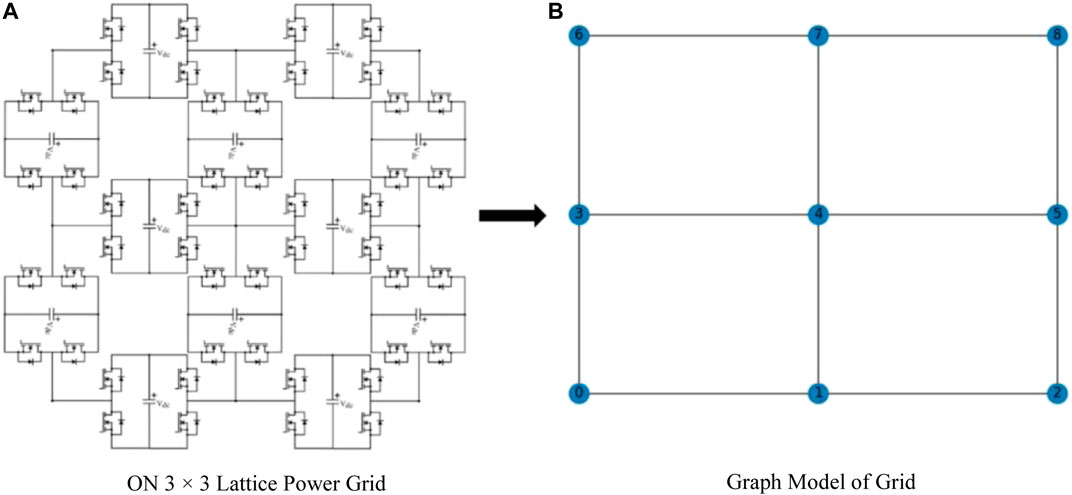
FIGURE 3. Square lattice grids and its graph model. (A) ON 3 × 3 lattice power grid. (B) Graph model of grid.
We model the lattice power grid architecture depicted in Figure 3 as a square lattice graph, whose topology forms a square regular tiling (Weisstein, 2021). The size of the graph is determined by the number of nodes along its height, n, and the number of nodes along its width, m. From Figure 3B,
To specify the location of a node, the graph can be considered as a coordinate system, with the coordinate (0, 0) representing the bottom-left node. If a node is located at coordinate
In other words, the bottom-left node is assigned to be the node number 0, and the node number counts upwards from left to right along each row. When the rightmost node of a row is reached, the next node counted is the leftmost node of the row directly above. The top-rightmost node is the highest-numbered, with node number mn − 1. This numbering system, applied to a 3 × 4 square lattice graph, is depicted in Figure 4. Individual edges/converters can be referenced by the two nodes adjacent to them. For instance, “edge 2–3” or “converter 2–3” can be equivalently used to reference the H-bridge converter connecting node 2 and node 3.
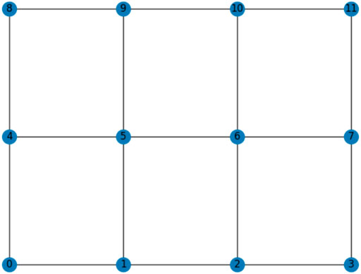
FIGURE 4. Node numberings for 3 × 4 lattice.
2.3 Triangular Lattice Power Grids and Their Graph Model
A triangular lattice graph is formed by a regular tiling of equilateral triangles. However, the rows of a triangular lattice can be shifted, as shown in Figure 5, so that the lattice lies on an m × n square arrangement of nodes. Thus, it is evident that an m × n triangular lattice is very similar to an m × n square lattice.
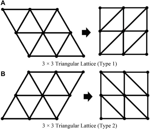
FIGURE 5. Triangular lattice graphs. (A) 3 × 3 Triangular lattice (Type 1). (B) 3 × 3 Triangular lattice (Type 2).
There are two embodiments of triangular lattices, which will be referred to as “type 1” and “type 2”, respectively. A type 1 triangular lattice is the one whose bottom left node has exactly three adjacent nodes, as shown in Figure 5A. In a type 2 triangular lattice, the bottom left node has exactly two adjacent nodes, as shown in Figure 5B.
2.4 Hexagonal Lattice Power Grids and Their Graph Mode
The nodes of a hexagonal lattice graph can also be shifted to lie in an m × n square arrangement, as shown in Figure 6. The hexagonal lattice takes on a “bricklaying” pattern. Vertical edges are connected in the same way as in a square lattice. However, a node is never connected horizontally to the right if there is already a node connected to its left. Furthermore, if a row begins with a pair of connected nodes, then the row above it must begin with a pair of unconnected nodes.

FIGURE 6. Hexagonal lattice graphs. (A) 4 × 4 Hexagonal lattice (Type 1). (B) 4 × 4 Hexagonal lattice (Type 2).
There are also two embodiments of hexagonal lattices. Type 1 has its bottom left node connected to exactly two other nodes, while type 2 has its bottom left node connected to exactly one other node (see Figure 6). In other words, the bottom row of a type 1 lattice begins with two connected nodes, while the bottom row of a type 2 lattice begins with two unconnected nodes.
2.5 Additional Lattice Types
This paper has discussed lattice power grids based on the three regular tilings: square, triangular, and hexagonal. However, the models and algorithms detailed in this paper are not limited to these three lattice types. As discussed later in Generalizing the Proposed Algorithms for Various Lattice Structures section, through the use of adjacency matrices, all of these concepts can be fully extended to any grid topology that is based on a simple, undirected graph. Several other lattice converter topologies have been proposed by Fang (2021b). In two dimensions, this includes the eight Archimedean tilings in addition to the three regular tilings. In three dimensions, novel lattice converters based on polyhedral tilings, or honeycombs, have been investigated as well. These include the cubic honeycomb lattice converter, as well as 28 lattice converter topologies based on Archimedean honeycombs (Fang, 2021b). Because these aforementioned topologies can all be represented using simple, undirected graphs and their adjacency matrices, the concepts discussed in this paper can be fully extended to them.
3 Objectives of the Proposed Control and Optimization Algorithms
This section details the objectives of lattice power grids. These include controlling grid-forming converters with a desired voltage difference between two nodes, allowing for enough current availability between those two nodes, and optimizing grid state changes while minimizing switching actions of power converters.
3.1 Voltage and Current Parameters
The goal is to create control and optimization algorithms that can satisfy a set of input parameters. Each node in a lattice power grid can be viewed as an I/O terminal. The algorithm should be able to accept two arbitrary nodes and create a desired voltage difference along a path between them. To carry an enough current between two nodes, it is sometimes necessary to create two or more paths in parallel between them, allowing for current sharing between the H-bridge voltage sources along the paths.
These are the two main objectives of any grid state outputted by the algorithm: achieving a desired voltage between two nodes and creating a desired number of parallel paths between them. Figure 7 depicts a grid state of a 4 × 4 square lattice power grid, where node 2 is the “start” node and node 13 is the “destination” node. Edges colored in blue represent H-bridge converters in the bypass mode (shorted), and edges in red represent converters in the ON state, either outputting +Vdc or −Vdc. Uncolored edges represent converters acting as an open circuit. In the grid state shown in Figure 7, there is a voltage difference of +3Vdc between the start and destination nodes, and three paralleled paths between them.
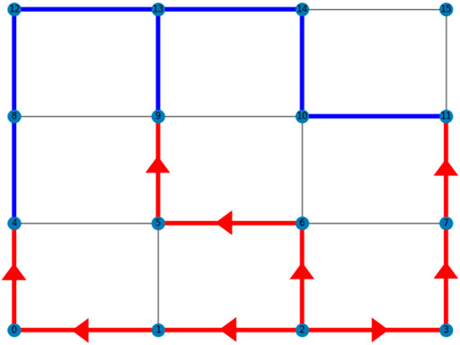
FIGURE 7. Example grid state for a 4 × 4 square lattice.
All converters that are outputting voltages should be creating a voltage increase along its path in the direction from start to destination. For example, along the leftmost path of Figure 7, there should be a voltage increase of Vdc from node 2 to node 1, another from node 1 to node 0, and another from node 0 to node 4, creating a total voltage increase of +3Vdc along the path.
A new convention can be introduced here to determine whether an individual H-bridge converter is in the positive output state or the negative output state. If the converter creates a voltage increase from the lower-numbered node to the higher-numbered node, it is in the positive output state. On the other hand, if the converter creates a voltage increase from the higher-numbered node to the lower-numbered node, it is in state 2. For instance, in Figure 7, converter 1–2 is outputting −Vdc, while converter 2–3 is outputting + Vdc.
3.2 Efficient Grid State Changes
Another objective can be considered when changing from one state to another. There may be multiple different states that fulfill the same parameters. If the lattice grid is in an initial state, and it is desirable to change states to fulfill a different set of parameters, there are often several possible end states to select from. The most efficient way to perform this change is by selecting the end state that requires the fewest number of individual converter-level state changes from the initial grid state. This is the final objective of the optimization algorithm.
4 Components of Control and Optimization Algorithms for Square Lattice Grids
This section details the development and the components of control and optimization algorithms for square lattice grids.
4.1 Creating a Square Lattice Graph
In the beginning, the lattice graph is implemented through a class called Graph. This class contains two main attributes: an integer representing the number of nodes in the graph and a dictionary indicating node adjacencies. If a graph contains v nodes, then its dictionary includes v keys
The Graph class also contains the function
To create an
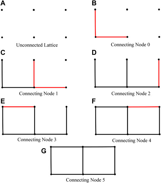
FIGURE 8. Formation of 2 × 3 square lattice. (A) Unconnected lattice. (B) Connecting node 0. (C) Connecting node 1. (D) Connecting node 2. (E) Connecting node 3. (F) Connecting node 4. (G) Connecting node 5.
4.2 Pathfinding Algorithm
The pathfinding component of the control and optimization algorithms will address the desired voltage difference parameter. The inputs to this algorithm are the desired dimensions m and n of the square lattice graph, the start and destination node numbers, and the desired voltage difference to be created between them.
Conceptually, to create a voltage difference between two nodes of +kVdc, where k is an integer, a path of length k or greater must be found between the nodes. If a path has length l, where
Two caveats will be addressed here; firstly, only integer values of k will be considered, as non-integer multiples of Vdc can be achieved through pulse-wave modulation. Secondly, it is not necessarily required that the first k edges in the path output voltage and the rest remain bypassed. It would be a valid solution to distribute the l − k bypassed edges in any possible way throughout the path. However, for the sake of simplicity and for preserving the efficiency of the algorithm, the only solutions that will be considered are those where all bypassed edges are located towards the end of the path, near the destination node.
The pathfinding algorithm itself, named findPaths, utilizes Depth-First Search (DFS) of a graph to search for viable paths (Goodrich and Tamassia, 2001; Yadav, 2021a; Yadav, 2021b). While traversing a graph, it is possible to visit the same node twice, which is not possible in a binary search tree. This must be avoided during DFS, so the algorithm also tracks which nodes have been visited (Yadav, 2021a). As the algorithm traverses the graph, visited nodes will be marked as such and will not be revisited. While the algorithm is backtracking, nodes removed from the path will again be marked as “unvisited,” allowing for new paths to be found.
This DFS algorithm traverses all possible paths through the graph originating from the start node. The other two input parameters to findPaths are the destination node number and the desired voltage difference k. With every edge traversal, findPaths checks if the current visited node is the same as the destination node. If this is the case, findPaths then checks whether this path from start to destination is of length k or greater. If both conditions are met, then the algorithm has found a viable path, which is stored in a list of lists. When the DFS algorithm has finished running, this list of lists contains all viable paths from start to destination and is returned by findPaths.
Suppose the inputs to findPaths are
Thus, there are four viable paths that meet the desired parameters in this example: three paths of length 3 and one path of length 5.
4.3 Parallel Paths Algorithm
The parallel paths component of the control and optimization algorithms, called currentPaths, will meet the requirement of current sharing. As real-world power converters are non-ideal and are limited by current ratings, it is often necessary to share current by connecting voltage sources in parallel. In the case of lattice grids, the amount of available current depends on the number of paralleled paths between the source and destination nodes.
For two paths to be considered parallel, they must meet at the start and destination nodes and cannot share any edges. Intersections between two or more paths are possible; however, at the point of intersection, all paths must yield the same voltage to avoid a conflict. Figure 7 depicts an example of a
The algorithm works as follows. Given an
Suppose that p is the desired number of paralleled paths. Then currentPaths arranges viable paths in permutations of size p. For each permutation, the algorithm iterates through each path contained in the permutation. The voltage of each node in the lattice is tracked and updated by the algorithm as it iterates through the paths. If a voltage conflict is detected between two paths in a permutation, then it is considered an invalid intersection and the permutation is discarded.
Furthermore, two parallel paths cannot share an edge. Thus, the algorithm also tracks which edges are occupied using an
Recall the example output from Pathfinding Algorithm section given by findPaths for a 2 × 3 square lattice graph with start node 0, destination node 5, and desired voltage difference 3:
Now, suppose that two parallel paths are desired to provide current sharing. Then, the four viable paths are placed in every possible permutation of size two, of which there are six:
1) [[0, 1, 2, 5], [0, 1, 4, 5]].
2) [[0, 1, 2, 5], [0, 3, 4, 1, 2, 5]]
3) [[0, 1, 2, 5], [0, 3, 4, 5]]
4) [[0, 1, 4, 5], [0, 3, 4, 1, 2, 5]]
5) [[0, 1, 4, 5], [0, 3, 4, 5]]
6) [[0, 3, 4, 1, 2, 5], [0, 3, 4, 5]]
Of these six permutations, the second and fourth can be discarded due to voltage. All except the third can also be discarded due to edge conflicts (e.g., edge 0–1 in permutation 1). The algorithm concludes that the two paths [0, 1, 2, 5] and [0, 3, 4, 5] from permutation 3 are in fact parallel and represent the only valid solution to the given parameters as no conflicts arose.
The algorithm in its current version assumes that paralleled paths start and end at the same nodes. Thus, the maximum number of paralleled paths is limited by the number of nodes adjacent to the start or destination nodes. The maximum number of paralleled paths can be theoretically increased through edge contraction, in which the start/destination nodes can be combined with neighboring nodes via short circuit (Belloch, 2012), essentially forming a “supernode” that can accommodate a greater number of paralleled paths. While not implemented in the current version of the algorithm, edge contraction represents a possible area for further exploration.
4.3 Least Changes of Converters Algorithm
The leastChanges algorithm deals with time-variant state changes of grid-forming converters. Assuming that the lattice power grid is in some initial state, it is then required to change the state to fulfill new objectives, then the most efficient way to do so is to select the end state that requires the smallest number of individual converter-level state changes, thus minimizing switching actions. In other words, out of all possible end states that fulfill the new objectives, the most efficient end state is the one that is the “most similar” to the initial state.
The “similarity” between two grid states can be compared using adjacency matrices. A grid consisting of v nodes will have an associated adjacency matrix of size v × v. In graph theory, adjacency matrices typically allow for two states: 0, indicating a pair of non-adjacent nodes, or 1, indicating an adjacency. However, as described in Fundamentals of Lattice Power Grids section, H-bridge converters can yield four possible states. Thus, the adjacency matrices introduced here also have four possible values for each element. 0 represents an open circuit, 1 and −1 represent an H-bridge converter outputting + Vdc and −Vdc, respectively, and 0.01 represents the bypass state, with the value chosen to represent a negligible voltage difference.
This adjacency matrix indicates the states of each H-bridge converter and will be referred to as the “path matrix.” This is meant to distinguish from the “graph matrix,” a separate adjacency matrix that is discussed later in Generalizing the Proposed Algorithms for Various Lattice Structures section. An example of the path matrix is depicted in Figure 9, where a grid state of a 3 × 3 lattice is shown in Figure 9A and its associated path matrix P is shown in Figure 9B.
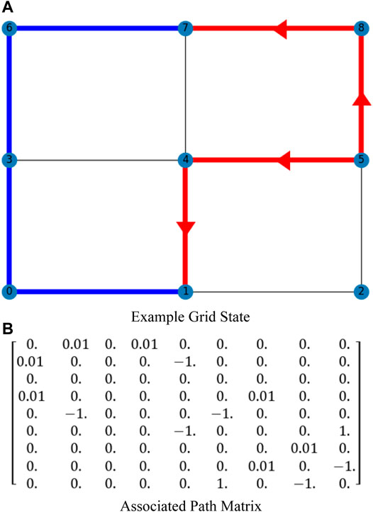
FIGURE 9. Example grid state and path matrix. (A) Example grid state. (B) Associated path matrix.
Each converter-level state change is associated with two changes in the path matrix (changing the state of edge a-b will change elements Pab and Pba in path matrix P). The leastChanges algorithm thus obtains the path matrix of the initial state, along with the path matrices of all viable path permutations outputted by currentPaths. The most efficient end state is the one whose path matrix has the fewest number of differences from the initial path matrix. If there are d differences between the initial and end path matrices, then d/2 converter state changes must have occurred.
Suppose that the state depicted in Figure 9A is taken to be the initial state. Then suppose that a set of new requirements is desired: +4Vdc voltage difference, only one current path, start node at node 0, and destination node at node 8. The end state selected by leastChanges and its associated path matrix are shown in Figure 10.
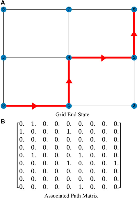
FIGURE 10. Example output of LeastChanges. (A) Grid end state. (B) Associated path matrix.
Out of all viable end states that fulfill the desired parameters, the state shown in Figure 10A is the one that requires the smallest number of converter-level state changes from the initial state. Seven converter-level state changes are required in this example (Note that edges 1–4 and 4–5 flipped in polarity).
4.5 Combined Algorithm
The components of the proposed control and optimizations algorithm can now be integrated into one. The final optimization algorithm runs on a while loop. On the first loop, the user is prompted for the dimensions m, n of the square lattice, and the graph is created using createGrid. The initial state on the first loop has all converters turned OFF, so all elements in its path matrix are filled with 0. The user then inputs desired specifications for the end state: start, destination, target voltage, and number of parallel paths. The algorithm calls findPaths and currentPaths to identify all path permutations that fulfill the parameters. These permutations are inputted into leastChanges, which identifies the most efficient end state.
The previous end state then becomes the new initial state. The algorithm can prompt the user to input new parameters, and the process can continue indefinitely. On each loop, the algorithm outputs the following: the path permutation of the end state, the path matrix of the end state, and the number of converter-level state changes from the initial state. The end state is then plotted using the networkx Python package.
5 Generalizing the Proposed Algorithms for Various Lattice Structures
5.1 Graph Matrices
To allow for the creation of arbitrary graphs, the “graph matrix” is introduced here. The graph matrix is another adjacency matrix that indicates which nodes are connected by H-bridge converters (edges). For a graph containing v nodes, its graph matrix will contain v × v elements. If an edge exists between nodes a and b, then element Gab and Gba will be filled with 1. Otherwise, it will be filled with 0. This is distinct from the path matrix described earlier, which indicates the state of each converter (+Vdc, −Vdc, shorted, or OFF).
The function used to create the desired graph matrix is called createGM (rather than createGrid). A graph matrix can be used to create a Graph object by iterating through each element of the matrix and using the addEdge function to connect nodes as directed. The graph matrix outputted by createGM is passed into findPaths, which uses it to create a Graph object, and the rest of the algorithm works exactly as described in Components of Control and Optimization Algorithms for Square Lattice Grids section.
Any simple, undirected graph can be created using graph matrices. Besides square lattice graphs, there exist two other types of lattice graphs: triangular and hexagonal. Creating a Triangular Lattice and Creating a Hexagonal Lattice sections explain how graph matrices can be used to generate triangular and hexagonal lattice graphs.
5.2 Creating a Square Lattice
The graph matrix for the square lattice graph is generated in exactly the same way as described in Creating a Square Lattice Graph section, except by filling in the elements of a graph matrix instead of directly using the addEdge function.
The process starts with an (m × n) × (m × n) matrix G, consisting of all zeroes. The createGM function iterates through all nodes in the graph. For a node with position (i, j) and node number
5.3 Creating a Triangular Lattice
Recall that a triangular lattice simply consists of diagonal connections added to a square lattice (see Figure 5). Thus, the procedure for forming a graph matrix for a triangular lattice graph matrix is the same as the procedure for a square lattice graph, with the addition of diagonal connections. For a type 1 triangular lattice, each node x is connected to the node directly to its top right if one exists. In other words, for a node with position (i, j) and node number
For a type 2 triangular lattice, each node x is connected to the node directly to its top left if one exists. In other words, graph matrix elements Gx,x+n−1 and Gx+n−1,x are flipped to 1 if
Upon repeating this process for every node in the lattice, createGM outputs the graph matrix for an m × n triangular lattice graph (see Figure 11).
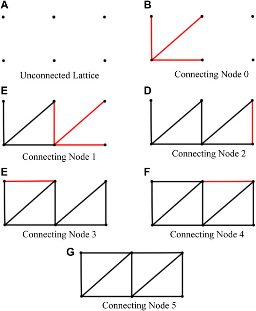
FIGURE 11. Formation of 2 × 3 triangular lattice. (A) Unconnected lattice. (B) Connecting node 0. (C) Connecting node 1. (D) Connecting node 2. (E) Connecting node 3. (F) Connecting node 4. (G) Connecting node 5.
5.4 Creating a Hexagonal Lattice
Recall that a hexagonal lattice can also be placed on a square arrangement of nodes (see Figure 6), forming a “brick” pattern. In this pattern, pairs of horizontally adjacent nodes alternate between being connected and unconnected across the rows and columns of the lattice.
This pattern is achieved through the addition of a Boolean value named connect, which determines whether the current node will be connected to the right. For a type 1 lattice, when createGM reaches the first node in any row i, connect is set to FALSE if the row is even (
Upon repeating this process for every node in the lattice, createGM outputs the graph matrix for an m x n hexagonal lattice graph (see Figure 12).
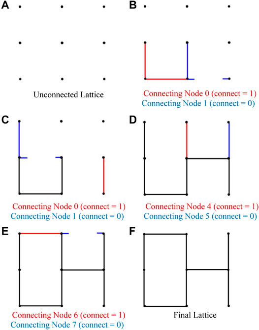
FIGURE 12. Formation of 3 × 3 hexagonal lattice. (A) Unconnected lattice. (B) Connecting node 0 (connect = 1), Connecting node 1 (connect = 0). (C) Connecting node 0 (connect = 1), Connecting node 1 (connect = 0). (D) Connecting node 4 (connect = 1), Connecting node 5 (connect = 0). (E) Connecting node 6 (connect = 1), Connecting node 7 (connect = 0). (F) Final lattice.
5.5 Final Optimization Algorithm
The final version of createGM essentially consists of six ‘if’ statements, one for each potential type of graph. If the user inputs “G” for “general,” createGM prompts the user to input the desired graph matrix row by row, allowing for any arbitrary graph. The user inputs “S” for a square lattice, “T1” or “T2” for a type 1 or type 2 triangular lattice, and “H1” or “H2” for a type 1 or type 2 hexagonal lattice. If the user inputs one of these lattice types, createGM will also prompt the user to input dimensions m and n of the lattice. The final output of createGM is the desired graph matrix.
The integrated optimization algorithm is the same as described in Components of Control and Optimization Algorithms for Square Lattice Grids section, except createGrid is replaced with createGM. The graph outputted by createGM is passed into findPaths, where all viable paths fulfilling the desired parameters are outputted. currentPaths then finds viable permutations of parallel paths. leastChanges determines which permutation requires the smallest number of converter-level changes from the initial state. This permutation is then printed and drawn. A flowchart of the overall control and optimization algorithms is depicted in Figure 13.
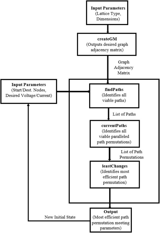
FIGURE 13. Flowchart of algorithms.
6 Simulations and Results
6.1 Simulations of the Lattice Grid
The lattice grid was simulated under the MATLAB Simulink/SimScape environment. The H-bridge converters were built with the “Full-Bridge Converter” block in SimScape (Mathworks, 2021). In the converter subsystem, the Full-Bridge Converter block is connected to a 1 kV DC voltage source for simplicity. It is given an on-state resistance of 10–3 Ω and a snubber resistance of 106 Ω, as well as an infinite snubber capacitance. A control signal entering the gating port consists of a 1 × 4 array controlling the four semiconductor switches in the converter (Mathworks, 2021). The matrices [0 1 1 0] and [1 0 0 1] correspond to the positive and negative ON-states, respectively. The matrix [1 0 1 0] (or [0 1 0 1]) corresponds to the bypass state, while [0 0 0 0] corresponds to the OFF-state.
Figure 14 shows the complete simulated model of a 3 × 4 square lattice power grid. In all, this model contains 17 H-bridge converter submodules, along with 17 × 4 gating signals to control them. As a 3 × 4 lattice contains 12 nodes, the path adjacency matrix (PAM) representing any given grid state will be a 12 × 12 matrix. Thus, the controller block is a MATLAB function block which accepts a 12 × 12 matrix as the input and demultiplexes it into 17 × 4 output gating signals. The grid state can then be set by inputting the appropriate path adjacency matrix into the controller block.

FIGURE 14. Simulated 3 × 4 lattice power grid with measurement apparatus.
6.2 Simulation Results
We inputted the following parameters into the control and optimization algorithms:
Enter the Desired Lattice Type: S
Enter the height m of the grid: 3
Enter the width n of the grid: 4
Enter the starting node number: 0
Enter the destination node number: 11
Enter the desired voltage difference: 3
Enter the desired number of paralleled paths: 1
These parameters returned a grid state and path adjacency matrix shown. This path adjacency matrix was placed into the model. An RLC load was connected between nodes 0 and 11 of the model, with a resistance of 5 Ω, an inductance of 10 mH. Voltage and current measurement blocks were connected accordingly as well (see Figure 14). (Note: In Figure 14, submodule blocks were colored in manually to indicate converter states).
The current and voltage measurements after running the simulation are shown in Figure 15. The results are as desired and expected, with the voltage difference between nodes 0 and 11 being +3 kV and the current approaching 0.6 kA by Ohm’s law. As there is only one path, the current rating of each submodule must be at least 0.6 kA for this grid state to be possible.
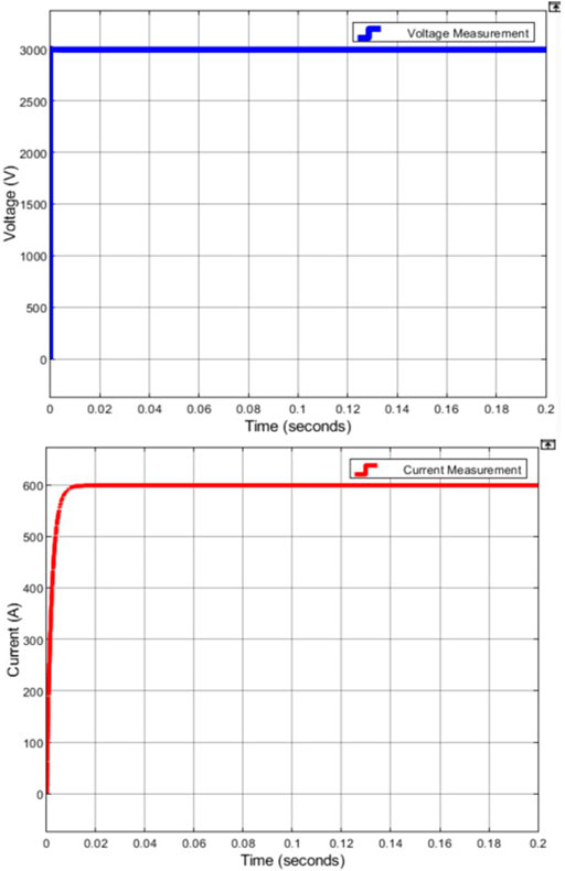
FIGURE 15. Simulated voltage and current measurements.
When measured between nodes 0 and 3, the voltage difference was found to be +3 kV. When measured between nodes 3 and 11, the voltage difference was found to be 0 V. This agrees with expectations, as submodules between nodes 3 and 11 are in the bypass state and do not output voltage.
7 Conclusion
This article proposes the concept of lattice power grids. Lattice power grids allow for serial and parallel connectivity of multiple grid-forming converters, thereby allowing both voltage and current sharing. Due to unparalleled voltage and current capabilities, lattice power grids are suitable for high-voltage applications and large-scale integration of renewable energies in more-electronics power systems. Specifically, this article proposes square, triangular, and hexagonal lattice power grids and their models by use of graph theory. More importantly, we propose a general control and optimization methodology and the relevant algorithms for various lattice power grids. The proposed lattice power grids can achieve current and voltage objectives while minimizing switching actions and maximizing system efficiency. Finally, simulation results validate the proposed lattice power grids as well as the control and optimization algorithms.
Data Availability Statement
The original contributions presented in the study are included in the article/Supplementary Material, further inquiries can be directed to the corresponding author.
Author Contributions
DZ was the primary author of this manuscript, created the algorithms described in the manuscript, and contributed to the proposed model of lattice power grids. JF provided significant guidance and mentorship for the direction and content of the research, and contributed to the proposed model of lattice power grids. He extensively reviewed and revised this manuscript and contributed expertise in many fields, including lattice power grids, lattice power converters, multilevel converters, and power systems. SG provided guidance and mentorship for the direction and content of research, reviewed and revised the manuscript, and contributed expertise in a variety of fields including lattice power grids, lattice power converters, multilevel converters, and power systems.
Conflict of Interest
The authors declare that the research was conducted in the absence of any commercial or financial relationships that could be construed as a potential conflict of interest.
Publisher’s Note
All claims expressed in this article are solely those of the authors and do not necessarily represent those of their affiliated organizations, or those of the publisher, the editors and the reviewers. Any product that may be evaluated in this article, or claim that may be made by its manufacturer, is not guaranteed or endorsed by the publisher.
References
Belloch, G. (2012). Parallel and Sequential Data Structures and Algorithms. Class Lecture, Topic: “Graph Contraction and Connectivity.”. Pittsburgh, PA: School of Computer Science, Carnegie-Mellon University.
Chappell, B. (2021). Renewable Energy Growth Rate up 45% Worldwide in 2020. IEA Sees New Normal,” National Public Radio. May 11, 2021. [Online]. Available at: https://www.npr.org/2021/05/11/995849954/renewable-energy-capacity-jumped-45-worldwide-in-2020-iea-sees-new-normal (Accessed Aug5, 2021).
Das, A. (2019a). High Power Multilevel Converters- Analysis, Design, and Operational Issues. Class Lecture, Topic: “Introduction to Multilevel Converters.”. IIT Delhi, Delhi, India: Department of Electrical Engineering.
Das, A. (2019b). High Power Multilevel Converters- Analysis, Design, and Operational Issues. Class Lecture, Topic: “Basic Understanding of Converter (Half Bridge and Full Bridge Circuit Operation).”. IIT Delhi, Delhi, India: Department of Electrical Engineering.
Deng, H., Qi, Y., Fang, J., Debusschere, V., and Tang, Y. (2021). Multi-Terminal Soft Open Point with Anti-islanding and Over-current Protection Capability. IEEE Energ. Convers. Congress Exposition. 2021, 745–750. doi:10.1109/ECCE47101.2021.9595456
Fang, J., Li, Z., and Goetz, S. M. (2021a). Multilevel Converters with Symmetrical Half-Bridge Submodules and Sensorless Voltage Balance. IEEE Trans. Power Electron. 36 (1), 447–458. Jan. 2021. doi:10.1109/TPEL.2020.3000469
Fang, J., Blaabjerg, F., Liu, S., and Goetz, S. (2021b). A Review of Multilevel Converters with Parallel Connectivity. IEEE Trans. Power Electron. 36 (11), 12468–12489. Nov. 2021. doi:10.1109/TPEL.2021.3075211
Fang, J., and Goetz, S. M. (2021). Symmetries in Power Electronics. Vancouver, British Columbia, BC, Canada: Proc. IEEE ECCE. 10–14 Oct. 2021.
Fang, J., Li, H., Tang, Y., and Blaabjerg, F. (2019). On the Inertia of Future More-Electronics Power Systems. IEEE J. Emerg. Sel. Top. Power Electron. 7 (4), 2130–2146. doi:10.1109/JESTPE.2018.2877766
Fang, J., Li, X., Tang, Y., and Hongchang, L. (2017). “Improvement of Frequency Stability in Power Electronics-Based Power Systems,” in 2017 Asian Conference on Energy, Power and Transportation Electrification (ACEPT), 1–6. doi:10.1109/ACEPT.2017.8168614
Fang, J. (2021a). More-Electronics Power Systems: Power Quality and Stability. Singapore: Springer Nature Singapore Pte Ltd.
Fang, J. (2021b). Unified Graph Theory-Based Modeling and Control Methodology of Lattice Converters. Electronics. 10 (17), 2146. doi:10.3390/electronics10172146
Flourentzou, N., Agelidis, V. G., and Demetriades, G. D. (2009). VSC-based HVDC Power Transmission Systems: An Overview. IEEE Trans. Power Electron. 24 (3), 592–602. Mar. 2009. doi:10.1109/tpel.2008.2008441
Goetz, S. M., Li, Z., Liang, X., Zhang, C., Lukic, S. M., and Peterchev, A. V. (2017). Control of Modular Multilevel Converter with Parallel Connectivity-Application to Battery Systems. IEEE Trans. Power Electron. 32 (11), 8381–8392. Nov. 2017. doi:10.1109/TPEL.2016.2645884
Goetz, S. M., Peterchev, A. V., and Weyh, T. (2015). Modular Multilevel Converter with Series and Parallel Module Connectivity: Topology and Control. IEEE Trans. Power Electron. 30 (1), 203–215. Jan. 2015. doi:10.1109/TPEL.2014.2310225
Goodrich, M., and Tamassia, R. (2001). “Graph Traversal” in Algorithm Design: Foundations, Analysis, and Internet Examples. Hoboken, NJ: Wiley, 303–316.
Han, D., Fang, J., Yu, J., Tang, Y., and Debusschere, V. (2019). “Small-Signal Modeling, Stability Analysis, and Controller Design of Grid-Friendly Power Converters with Virtual Inertia and Grid-Forming Capability,” in 2019 IEEE Energy Conversion Congress and Exposition (ECCE), 27–33. doi:10.1109/ECCE.2019.8912534
Hooshyar, H., and Vahedi, M. A. (2007). Synchronous Generator: Past, Present and Future. AFRICON. 2007, 1–7. doi:10.1109/AFRCON.2007.4401482
Lin, Y. (2020). Research Roadmap on Grid-Forming Inverters. Golden, CO: National Renewable Energy Laboratory. [Online]. Available at: https://www.nrel.gov/docs/fy21osti/73476.pdf.
Mathworks (2021). Full-Bridge Converter,” mathworks.Com. [Online] Available at: https://www.mathworks.com/help/physmod/sps/powersys/ref/fullbridgeconverter.html (Accessed Jun 27, 2021).
Mei, Z., Fang, J., and Goetz, S. (2022). Control and Optimization of Lattice Converters. Electronics. 11 (4), 594. doi:10.3390/electronics11040594
U.S. Department of Energy Office of Energy Efficiency and Renewable Energy (2018). 2018 Renewable Energy Data Book.” [Online]. Available at: https://www.nrel.gov/docs/fy20osti/75284.pdf (Accessed August 5, 2021).
Weisstein, E. W. (2021). Lattice Graph,” Wolfram Mathworld. [Online]. Available at: https://mathworld.wolfram.com/LatticeGraph.html (Accessed Aug 5, 2021).
Yadav, N. (2021a). Depth First Search or DFS for a Graph. geeksforgeeks.org, Jul 22, 2021. [Online]. Available at: https://www.geeksforgeeks.org/depth-first-search-or-dfs-for-a-graph (Accessed Jan 20, 2021).
Yadav, N. (2021b). Print All Paths from a Given Source to a Destination. geeksforgeeks.org, Jul 2, 2021. [Online]. Available at: https://www.geeksforgeeks.org/depth-first-search-or-dfs-for-a-graph (Accessed Jan 20, 2021).
Keywords: H-bridge converters, multilevel converters, lattice power grids, power systems, renewable energies
Citation: Zhang DW, Fang J and Goetz S (2022) Control and Optimization Algorithms for Lattice Power Grids With Multiple Grid-Forming Converters. Front. Energy Res. 10:878592. doi: 10.3389/fenrg.2022.878592
Received: 18 February 2022; Accepted: 31 March 2022;
Published: 04 May 2022.
Edited by:
Peng Li, Tianjin University, ChinaCopyright © 2022 Zhang, Fang and Goetz. This is an open-access article distributed under the terms of the Creative Commons Attribution License (CC BY). The use, distribution or reproduction in other forums is permitted, provided the original author(s) and the copyright owner(s) are credited and that the original publication in this journal is cited, in accordance with accepted academic practice. No use, distribution or reproduction is permitted which does not comply with these terms.
*Correspondence: Jingyang Fang, amluZ3lhbmdmYW5nQHNkdS5lZHUuY24=