
94% of researchers rate our articles as excellent or good
Learn more about the work of our research integrity team to safeguard the quality of each article we publish.
Find out more
ORIGINAL RESEARCH article
Front. Energy Res., 22 February 2022
Sec. Solar Energy
Volume 10 - 2022 | https://doi.org/10.3389/fenrg.2022.840817
This article is part of the Research TopicEco-friendly Chalcogenide and Perovskite Based Materials for Solar Energy ConversionView all 4 articles
This work reported the successive incorporation of tetrabutylammonium (TBA) into Methylammonium lead Iodide (MAPbI3) perovskite. The thin films were characterized by X-Ray diffraction (XRD), Scanning electron microscopy (SEM), Transmittance electron microscopy (TEM), Atomic force microscopy (AFM), and UV-Visible spectroscopy. It was shown that introducing TBA increases the crystallinity, grain size, surface morphology without pin-hole, and roughness of the MAPbI3 thin films. Moreover, the MA(1-X)TBAX PbI3 thin film shows better stability in a relative humidity of ∼60% after 15 days than the pure MAPbI3 thin film. The obtained results are hoped to be helpful for stability and improvement of the performance of the MAPbI3 thin films by doping TBA cations under ambient conditions.
⁃ The MA(1-X)TBAX PbI3 thin film crystallinity was enhanced with TBA incorporation.
⁃ The morphology of MAPbI3 improved with a pinhole-free surface.
⁃ Optical and PL properties were boosted with the TBA incorporation into MAPbI3 thin film.
⁃ MA(1-X)TBAX PbI3 thin film shows better stability than pure MAPbI3 thin film.
To begin with, nowadays, the Perovskites with formula ABX3 (A = cation (Formamidinium (FA), Methylammonium (MA).), B = metal cation and X is a halogen anion VII halides (Br−, Cl−, I−)), have been demonstrated good absorbers properties for solar cells with higher photovoltaic conversion efficiency (PCE) (Fakharuddin et al., 2019; Weidman et al., 2019). Methylammonium lead triiodide (MAPbI3) solar cells show good optoelectronic properties with a bandgap between 1.4 and 1.5 eV (Wang et al., 2019), a high absorption coefficient around 105cm−1 (Im et al., 2011; De Roo et al., 2016) with amazing PCE = 25% (Xiao et al., 2014; Park, 2015). To manufacture MAPbI3 Solar cells, low-cost and simple techniques have been used to deposit the MAPbI3 film: thermal vapor deposition, two-step vapor-assisted deposition (Chen et al., 2013), two-step solution deposition, and one-step solution deposition (Yantara et al., 2015; Patel et al., 2017). Despite the outstanding PCE reported of MAPbI3 solar cells, the problem of MAPbI3 degradation by the loss of MAI and formation of lead iodide PbI2 under humid conditions and higher temperatures makes use of MAPbI3 difficult (Ko et al., 2015). Concerning to improve the stability of MAPbI3, MAPbI3 was doped by cesium and showed the potential to enhance the stability of MaPbI3 solar cell under UV irradiance conditions (Niu et al., 2016); also on the road for stable MAPbI3, the divalent anion Se2− was incorporated in MAPbI3 structure to increase the atomic interactions between the inorganic and the organic cations (Gong et al., 2018; Li et al., 2018). Considering the ongoing discussion, some researchers have demonstrated that the MAPbBr3 absorber is more stable than MAPbI3; the MAPbBr3 optical absorption is not appropriate for solar cell production (Ahmad et al., 2019).
In this research work, the tetrabutylammonium iodide (TBA) was incorporated into MAPbI3 solution in the form of MA(1-X)TBA(X) PbI3 thin film to study the effect on the structure-property of the MAPbI3 when TBA was incorporated in different percentages. As a result, significant improvement was found in the crystallinity, morphology, optical properties, and stability of the MA(1-X)TBA(X) PbI3 thin film. The obtained results are hoped to help delay the degradation and to enhance the performance of the MAPbI3 thin film by doping TBA cations under ambient conditions.
Methylammonium iodide (MAI), Lead (II) iodide (PbI2), Chlorobenzene (CBZ), Methylammonium iodide (MAI) and Tetrabutylammonium iodide (TBAI), anhydrous N,N-dimethylformamide (DMF) and dimethyl sulfoxide (DMSO). All compounds were purchased from Sigma-Aldrich, and they were used without any additional purification. The MA1−xTBAxPbI3 solution was prepared in a glovebox by dissolving PbI2, TBAI, and MAI in the solvent of DMF and DMSO; the solution was agitated at 60°C for 3 h.
X-ray diffraction (XRD) was employed to characterize the crystallinity of the films using RIGAKU Ultima IV diffractometer the range of 2θ = 10°–60° using CuKa radiation (λ = 1.5418 Å) at room temperature. The morphology characteristic of thin films was constantly observed by scanning electron microscopy (SEM) model (Quanta 200–FEI) under 1.5 kV accelerated potential in several magnifications (Stewart et al., 2021). In addition, the films were examined by atomic force microscopy (AFM) with 0.5Hz a scan rate. The fringes crystallinity was confirmed by Transmission electron microscopy with 2.5 KV. Also, UV-VIS and PL spectra were characterized using Ocean Optics HR4000 spectrophotometer in the range of 300–850 nm and He-Cd laser source Si-CCD detector Hamamatsu for PL analysis, respectively.
In the present work, thin films perovskite MA1−xTBAxPbI3 were successfully deposited on FTO back contact using a simple spin-coating technique. Figure 1 shows the XRD results of the MA1−xTBAxPbI3 where X = (0, 1,2.5, 5, 10). The characteristic peaks located at 14° and 28° match to XRD planes of (110) and (220) respectively in agreement with MAPbI3 structure (Ono et al., 2015; Abdelmageed et al., 2016) without any PbI2 binary phase. Thus, a significant increase was found in the main XRD peaks (110) and (220) intensities and crystallinity by incorporating the TBA amount. Figure 2 represents the zoomed XRD peak in the range of 13°–15°; the small shift was observed towards a lower 2θ degree after the incorporation of TBA compared to the MAPbI3 thin film. Furthermore, the increase in the crystal lattice could be related to a bigger radius TBA (4.70 Å) than a small radius of MA (1.8 Å).
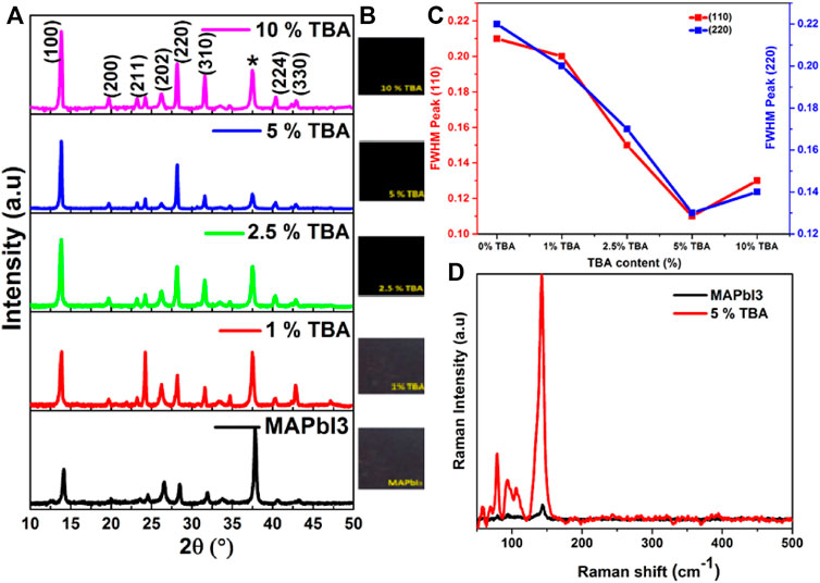
FIGURE 1. (A) XRD pattern of MA1−xTBAxPbI3 where X%= (0, 1, 2.5,5, and 10), (B) MA1−xTBAxPbI3 photographs (C) FWHM of (011) and (022) peaks of MA1−xTBAxPbI3 (C) Raman spectra of MAPbI3 undoped and doped with 5% TBA.
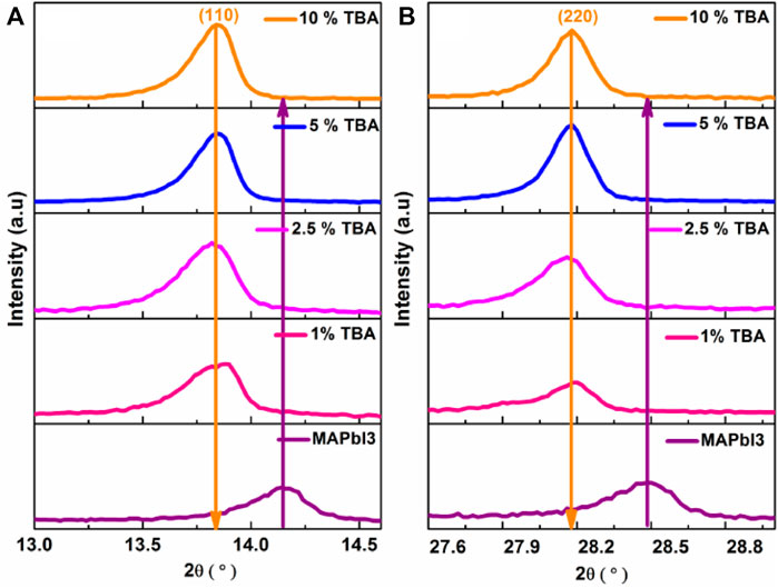
FIGURE 2. The zoomed XRD peaks, (A) (110) and, (B) (220) of MA1−xTBAxPbI3 where X % = (0%, 1%, 2.5%, 5%, and 10%).
The MAPbI3 thin film with a tetragonal structure where a = b = 8.90 Å, c = 11.12 Å and with insignificant changes due to TBA incorporation where a = b = 8.91 Å, c = 11.11 Å. The crystal parameters details of MA1−xTBAxPbI3 and the grain size were calculated using the Pawley method summarized in Table 1. Moreover, FWHM of peaks (110) and (220) values gradually decrease an agreement of good crystallinity of the films with increasing the amount of TBA from 0 to 5% in Figure 1C. In this respect, the stability of the MAPbI3 main (110) peak remains excellent after incorporating TBA amounts. Especially many studies have been reported that the inorganized Pb atoms affect the surface imperfections of the film, which leads to a decrease in the performance of perovskite devices. In the current work, the TBA arguably shows a significant improvement of MAPbI3 stability that degrades quickly into PbI2 in external conditions (Yu et al., 2018).
Here, the Raman spectroscopy analysis was used to verify the phase identification of pure MAPbI3 and 5% doped TBA Figure 1D. The dominants two vibrational modes were identified for MAPbI3 approximately at 68 cm−1 and 142 cm−1. The intensities of the same vibrational mode increased after incorporating 5% TBA content. The 68 and 142 cm−1 bands matched with the obtained results from XRD that confirmed the incorporation of TBA, which plays a vital role in the formation of crystallinity (Fateev et al., 2018).
Figure 3 illustrates the SEM images of MA1−xTBAxPbI3 where X % (0%, 1%, 2.5%, 5%, 10%). The undoped MAPbI3 shows a small grain size with a smooth surface and good distribution of lead and iodide (Chen et al., 2018). In the same way, the TBA incorporation increase gradually grain size of 210 nm for pure MAPbI3, 290 nm for the doped MAPbI3 with 1.0% TBA, 490 nm for 2.50% TBA as well as with a higher value of 500 nm for 5.0% TBA figure (a–d). This improvement of the grain size of doped MAPbI3 can be due to the crystal growth by decreasing crystal nucleation and lead to good surface coverage and higher crystallinity, as shown by the XRD analysis (Banerjee and Chattopadhyay, 2018; Liu et al., 2020). In this connection, the enhanced crystallinity and grain size could be attributed to fewer defects in the trap state, decreasing the non-radiative recombination in the MAPbI3 surface (Guo et al., 2019).
The specimen preparation technique used for perovskite samples prepared is tripod polishing for perovskite for high-resolution TEM investigation, scratching the perovskite film prepared and putting it in the special grid of aluminum to characterize the samples with TEM analysis, Figure 4 displays TEM analysis of pure MAPbI3 and doped with 5% TBA expose the scattered through lattice fringes spacing of 13.10 Å correspond to [110] crystallographical plan as well as 7.60 Å match with [220] crystallographical respectively. The selected portion of the electron diffraction spectrum shows that pure and 5% TBA doped MAPbI3 films are polycrystalline, where is in good agreement with XRD results (Giesbrecht et al., 2018; Jones et al., 2019).
Figure 5 shows AFM images with 2 and 3 Dimension of undoped and doped MAPbI3, where the measured roughness is varying, that offers a change compared to doped and undoped MAPbI3 where RMS= (147.7, 198, and 168 nm) calculated for the x% TBA where x = (0, 5 and 10) respectively which is measured by the root-mean-square (RMS) (Table 1). Moreover, the RMS value of 10% TBA doped MAPbI3 shows a slight decrease than the incorporation of 5% of TBA, showing the optimum level for large grain size and high roughness in the AFM analysis (Tombe et al., 2018).
This experiment performed the optical absorption and photoluminescence measurements for MAPbI3 thin film doped TBA to analyze the optoelectronic properties. Here, Figure 6A illustrates the optical absorption of MAPbI3 pure and doped TBA from 400 to 900 nm wavelength, where the optical bandgap was estimated around 1.55–1.59 eV. Upon monitoring carefully, the variation in the optical bandgap was observed by incorporating the TBA amount (Smith et al., 2019). This significant improvement could be related to pinhole-free TBA doped MAPbI3 films, as shown in SEM analysis (Sun et al., 2017).
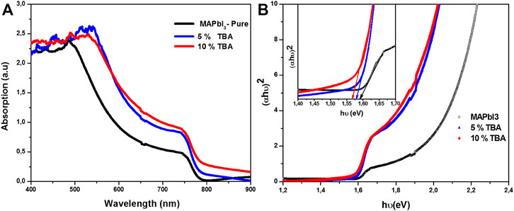
FIGURE 6. (A) Optical absorption, (B) calculated bandgap of MA1−xTBAxPbI3 where X % = (0%, 5%, and 10%).
Besides, Figure 7 shows the photoluminescence spectrum of undoped MAPbI3 and doped TBA, where the FWHM intensity progressively increases with the increase of TBA content. Doped 5% TBA represents a significantly higher red emission around 55 nm. This emission is three times higher than undoped MAPbI3 thin film. The results could be attributed to reducing trap density states with decreased charge recombination, which improved the thin film’s optoelectronic properties (Brennan et al., 2017; Ngo et al., 2018).
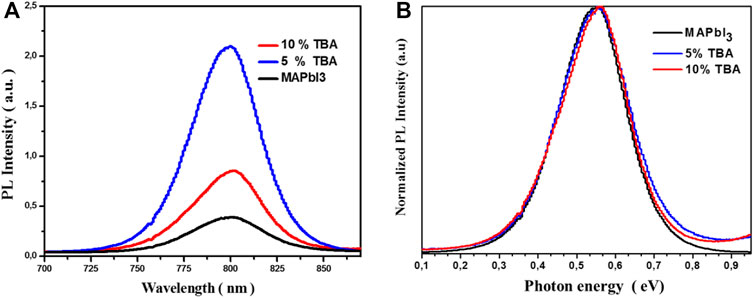
FIGURE 7. (A) PL spectra and (B) is the normalized PL spectra of MA1−xTBAxPbI3 where X % = (0%, 5%, and 10%) thin film.
In this context, one of the essential parameters of semiconductor materials is the stokes shift. This shift was observed between the optical absorption edge and PL peak. The comparison of stoke shift values is summarized in Table 2. The stoke shift describes the reduction of lattice parameters in the crystals. The low value of the stoke shift indicates the good photophysical properties of MAPbI3 (Bouich et al., 2021a; Bouich et al., 2021b).
The degradation of pure MAPbI3 and 5% doped TBA samples were examined under a dark relative 60% humidity environment where samples were stored for 15 days. Consequently, a significant transformation from the black color to the yellow color was observed for the pure MAPbI3 aged sample after 2 weeks which indicated the dissociation of MAPbI3 to PbI2 confirmed by yellow color compared to 5% doped TBA aged sample was less affected (Figure 9).
Figure 8 illustrates the SEM images of the MAPbI3 surface were affected by humidity and the water molecules over the grain boundaries, which led to the degradation of MAPbI3 and the formation of PbI2 and MAI. The TBA cation reduced the grain boundaries to prevent the access of humidity into the film. Furthermore, the 5% TBA doped MAPbI3 has shown a slight crystal structure distortion than the pure MAPbI3 (Huang et al., 2017; Kundu and Timothy, 2020).
Figure 9 displays the XRD patterns and the structural variations through the degradation of the doped and undoped MAPbI3 with the characteristic peak (110) of pure MAPbI3 shows dramatically reduced; however, the 5% TBA doped MAPbI3 thin film observed less affected by the environment as compared to pure MAPbI3.
Furthermore, the environmental effect was studied from the UV-Visible analysis of the 5% TBA doped MAPbI3; Figure 10 shows a slow-down variation in the absorption edge, and the color changed from dark to brown of the sample after 2 weeks in relative humidity (60%). The obtained results confirm that incorporating TBA into the MAPbI3 could decrease the degradation of the methylammonium lead triiodide absorber for photovoltaic application.
As we noticed a change in the bandgap of doped with 5% TBA and undoped MAPbI3 has been observed. The effect of thickness and bandgap variation of the absorber layer has a more significant impact on the performance of solar cells. We simulate a proposed solar cell having a model “Gold/SpiroOmTAD/MAPbI3/TiO2/FTO/Glass” to keep this impact on the cell’s performance. Here Gold is used as a front contact, OmTAD as ETL, MAPbI3 as an absorber layer, TiO2 as HTL, F.T.O is working as a back contact, and glass is a substrate (Kundu and Timothy, 2020; Mesbahi et al., 2021; Quan et al., 2019).
Figure 11C show the J-V characteristics curve and clearly show the effect of doped and undoped MAPbI3, Voc was 0.95V, Jsc of 22.4 mA/cm2, FF of 87.1%, and Eta of 18.01% recorded. Here we note that undoped is giving less performance, Voc, Jsc, FF, and Eta were registered as 0.85V, 25.7 mA/cm2, 86.1%, and 20.42%, respectively, which was good as compared to the results of the film growth and crystallinity (Table 3 and Table.1 in Supplementary Materials).
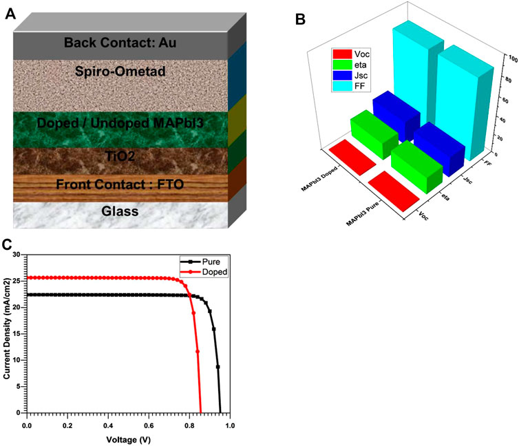
FIGURE 11. (A) diagram of MAPbI3 based solar cell (B) Characteristics Parameters Comparison of MAPbI3 based solar cell (C) JV characteristics curves of MAPbI3 based solar cell.
To sum up, from the preceding discussion, it appears that the doped with a small amount of TBA significantly increases the morphology and stability of MAPbI3 thin film for photovoltaic applications. The XRD analysis revealed that the crystallinity of MAPbI3 thin film enhanced with TBA, the TBA affects leading MAPbI3 film with a homogenous, highly rough surface and large grain size, which could cause trap more light in the surface. Similarly, the MA(1-X)TBAXPbI3 thin film shows better stability in a relative humidity of ∼60% after 15 days than pure MAPbI3 thin film. The obtained results are hoped to help delay the degradation and to enhance the performance of the MAPbI3 thin film by doping TBA cations under ambient conditions.
The original contributions presented in the study are included in the article/Supplementary Material, further inquiries can be directed to the corresponding author.
Conceptualization AB; methodology, AB; validation BS formal analysis, JM-G; investigation PP resources AB data curation, AB; writing—original draft preparation, JM-G; writing—review and editing, AB, BM; visualization, AB; supervision, BM; project administration, funding acquisition, BM. All authors have read and agreed to the published version of the manuscript.
This work was supported by the Ministerio de Economia y Competitividad (ENE 2016-77798-C4-2-R). Author AB acknowledged the Post-doctoral contract supported by the RRHH, the Postdoctoral contract the Margarita Salas financed with union European Next Generation EU. Grant PID2019-107137RB-C21 and PID2019-107137RB-C22OAQ funded by MCIN/AEI/10.13039/501100011033 and by “ERDF A way of making Europe.
The authors declare that the research was conducted in the absence of any commercial or financial relationships that could be construed as a potential conflict of interest.
All claims expressed in this article are solely those of the authors and do not necessarily represent those of their affiliated organizations, or those of the publisher, the editors, and the reviewers. Any product that may be evaluated in this article, or claim that may be made by its manufacturer, is not guaranteed or endorsed by the publisher.
The Supplementary Material for this article can be found online at: https://www.frontiersin.org/articles/10.3389/fenrg.2022.840817/full#supplementary-material
Abdelmageed, G., Jewell, L., Hellier, K., Seymour, L., Luo, B., Bridges, F., et al. (2016). Mechanisms for Light Induced Degradation in MAPbI3 Perovskite Thin Films and Solar Cells. Appl. Phys. Lett. 109 (23), 233905. doi:10.1063/1.4967840
Ahmad, Z., Shikoh, A. S., Paek, S., Nazeeruddin, M. K., Al-Muhtaseb, S. A., Touati, F., et al. (2019). Degradation Analysis in Mixed (MAPbI3 and MAPbBr3) Perovskite Solar Cells under thermal Stress. J. Mater. Sci. Mater. Electron. 30 (2), 1354–1359. doi:10.1007/s10854-018-0403-4
Banerjee, D., and Chattopadhyay, K. K. (2018). “Hybrid Inorganic Organic Perovskites,” in Perovskite Photovoltaics (Academic Press), 123–162. doi:10.1016/b978-0-12-812915-9.00005-8
Bouich, A., Ullah, S., Marí, B., Atourki, L., and Touhami, M. E. (2021a). One-step Synthesis of FA1-xGAxPbI3 Perovskites Thin Film with Enhanced Stability of Alpha (α) Phase. Mater. Chem. Phys. 258, 123973. doi:10.1016/j.matchemphys.2020.123973
Bouich, A., Mari, B., Atourki, L., Ullah, S., and Touhami, M. E. (2021b). Shedding Light on the Effect of Diethyl Ether Antisolvent on the Growth of (CH3NH3) PbI3 Thin Films. JOM 73 (2), 551–557. doi:10.1007/s11837-020-04518-5
Brennan, M. C., Zinna, J., and Kuno, M. (2017). Existence of a Size-dependent Stokes Shift in CsPbBr3 Perovskite Nanocrystals. ACS Energ. Lett. 2 (7), 1487–1488. doi:10.1021/acsenergylett.7b00383
Chen, L.-C., Lee, K.-L., Wu, W.-T., Hsu, C.-F., Tseng, Z.-L., Sun, X. H., et al. (2018). Effect of Different CH3NH3PbI3 Morphologies on Photovoltaic Properties of Perovskite Solar Cells. Nanoscale Res. Lett. 13 (1), 140. doi:10.1186/s11671-018-2556-8
Chen, Q., Zhou, H., Hong, Z., Luo, S., Duan, H.-S., Wang, H.-H., et al. (2013). Planar Heterojunction Perovskite Solar Cells via Vapor-Assisted Solution Process. J. Am. Chem. Soc. 136 (2), 622–625. doi:10.1021/ja411509g
De Roo, J., Ibáñez, M., Geiregat, P., Nedelcu, G., Walravens, W., Maes, J., Martins, J. C., Van Driessche, I., Kovalenko, M. V., and Hens, Z. (2016). Highly Dynamic Ligand Binding and Light Absorption Coefficient of Cesium lead Bromide Perovskite Nanocrystals. ACS Nano 10 (2), 2071–2081. doi:10.1021/acsnano.5b06295
Fakharuddin, A., Shabbir, U., Qiu, W., Iqbal, T., Sultan, M., Heremans, P., et al. (2019). Inorganic and Layered Perovskites for Optoelectronic Devices. Adv. Mater. 31 (47), 1807095. doi:10.1002/adma.201807095
Fateev, S. A., Petrov, A. A., Khrustalev, V. N., Dorovatovskii, P. V., Zubavichus, Y. V., Goodilin, E. A., et al. (2018). Solution Processing of Methylammonium Lead Iodide Perovskite from γ-Butyrolactone: Crystallization Mediated by Solvation Equilibrium. Chem. Mater. 30 (15), 5237–5244. doi:10.1021/acs.chemmater.8b01906
Giesbrecht, N., Schlipf, J., Grill, I., Rieder, P., Dyakonov, V., Bein, T., et al. (2018). Single-crystal-like Optoelectronic-Properties of MAPbI3 Perovskite Polycrystalline Thin Films. J. Mater. Chem. A. 6 (11), 4822–4828. doi:10.1039/c7ta11190h
Gong, J., Yang, M., Rebollar, D., Rucinski, J., Liveris, Z., Zhu, K., et al. (2018). Divalent Anionic Doping in Perovskite Solar Cells for Enhanced Chemical Stability. Adv. Mater. 30 (34), 1800973. doi:10.1002/adma.201800973
Guo, P., Ye, Q., Yang, X., Zhang, J., Xu, F., Shchukin, D., and Wang, H. (2019). Surface & Grain Boundary Co-passivation by Fluorocarbon-Based Bifunctional Molecules for Perovskite Solar Cells Efficiency over 21%. J. Mater. Chem. A 7 (6), 2497–2506. doi:10.1039/c8ta11524a
Huang, J., Tan, S., Lund, P. D., and Zhou, H. (2017). Impact of H2O on Organic-Inorganic Hybrid Perovskite Solar Cells. Energ. Environ. Sci. 10 (11), 2284–2311. doi:10.1039/c7ee01674c
Im, J. H., Lee, C. R., Lee, J. W., Park, S. W., and Park, N. G. (2011). 6.5% Efficient Perovskite Quantum-Dot-Sensitized Solar Cell. Nanoscale 3 (10), 4088–4093. doi:10.1039/c1nr10867k
Jones, T. W., Osherov, A., Alsari, M., Sponseller, M., Duck, B. C., Jung, Y.-K., et al. (2019). Lattice Strain Causes Non-radiative Losses in Halide Perovskites. Energy Environ. Sci. 12 (2), 596–606. doi:10.1039/c8ee02751j
Ko, H. S., Lee, J. W., and Park, N. G. (2015). 15.76% Efficiency Perovskite Solar Cells Prepared under High Relative Humidity: the Importance of PbI2 Morphology in Two-step Deposition of CH3 NH3 PbI3. J. Mater. Chem. A 3 (16), 8808–8815. doi:10.1039/c5ta00658a
Kundu, S., and Timothy, L. K. (2020). In Situ studies of the Degradation Mechanisms of Perovskite Solar Cells. EcoMat 2 (2), e12025. doi:10.1002/eom2.12025
Li, J., Jiu, T., Duan, C., Wang, Y., Zhang, H., Jian, H., et al. (2018). Improved Electron Transport in MAPbI3 Perovskite Solar Cells Based on Dual Doping Graphdiyne. Nano Energy 46, 331–337. doi:10.1016/j.nanoen.2018.02.014
Liu, C., Cheng, Y.-B., and Ge, Z. (2020). Understanding of Perovskite crystal Growth and Film Formation in Scalable Deposition Processes. Chem. Soc. Rev. 49 (6), 1653–1687. doi:10.1039/c9cs00711c
Marí-Guaita, J., Bouich, A., Shafi, M. A., Bouich, A., and Marí, B. Investigation on the stability and efficiency of MAPbI3 and MASnI3 thin films for Solar Cells. Physica Status Solidi (a)
Mesbahi, O., Tlemçani, M., Janeiro, F. M., Hajjaji, A., and Kandoussi, K. (2021). Sensitivity Analysis of a New Approach to Photovoltaic Parameters Extraction Based on the Total Least Squares Method. Metrology Meas. Syst.,28 751–765. doi:10.24425/mms.2021.137707
Ngo, T. H., Gil, B., Shubina, T. V., Damilano, B., Vezian, S., Valvin, P., et al. (2018). Enhanced Excitonic Emission Efficiency in Porous GaN. Sci. Rep. 8 (1), 15767–15769. doi:10.1038/s41598-018-34185-1
Niu, G., Yu, H., Li, J., Wang, D., and Wang, L. (2016). Controlled Orientation of Perovskite Films through Mixed Cations toward High Performance Perovskite Solar Cells. Nano Energy 27, 87–94. doi:10.1016/j.nanoen.2016.06.053
Ono, L. K., Raga, S. R., Remeika, M., Winchester, A. J., Gabe, A., and Qi, Y. (2015). Pinhole-free Hole Transport Layers Significantly Improve the Stability of MAPbI3-Based Perovskite Solar Cells under Operating Conditions. J. Mater. Chem. A. 3 (30), 15451–15456. doi:10.1039/c5ta03443d
Park, N.-G. (2015). Perovskite Solar Cells: an Emerging Photovoltaic Technology. Mater. Today 18 (2), 65–72. doi:10.1016/j.mattod.2014.07.007
Patel, J. B., Wong‐Leung, J., Van Reenen, S., Sakai, N., Wang, J. T. W., Parrott, E. S., et al. (2017). Influence of Interface Morphology on Hysteresis in Vapor‐Deposited Perovskite Solar Cells. Adv. Electron. Mater. 3 (2), 1600470. doi:10.1002/aelm.201600470
Quan, L. N., Rand, B. P., Friend, R. H., Mhaisalkar, S. G., Lee, T.-W., and Sargent, E. H. (2019). Perovskites for Next-Generation Optical Sources. Chem. Rev. 119 (12), 7444–7477. doi:10.1021/acs.chemrev.9b00107
Smith, M. D., Connor, B. A., and Karunadasa, H. I. (2019). Tuning the Luminescence of Layered Halide Perovskites. Chem. Rev. 119 (5), 3104–3139. doi:10.1021/acs.chemrev.8b00477
Stewart, A. W., Bouich, A., and Soucase, B. M. (2021). Enhancing the stability and crystallinity of CsPbIBr2 through antisolvent engineering. J. Mater. Sci. 56 (36), 20071–20086.
Sun, C., Guo, Y., Fang, B., Guan, L., Duan, H., Chen, Y., et al. (2017). Facile Preparation of High-Quality Perovskites for Efficient Solar Cells via a Fast Conversion of Wet PbI2precursor Films. RSC Adv. 7 (36), 22492–22500. doi:10.1039/c7ra03066e
Tombe, S., Adam, G., Heilbrunner, H., Yumusak, C., Apaydin, D. H., Hailegnaw, B., et al. (2018). The Influence of Perovskite Precursor Composition on the Morphology and Photovoltaic Performance of Mixed Halide MAPbI3-xClx Solar Cells. Solar Energy 163, 215–223. doi:10.1016/j.solener.2018.01.083
Wang, Y., Fang, W.-H., Long, R., and Prezhdo, O. V. (2019). Symmetry Breaking at MAPbI3 Perovskite Grain Boundaries Suppresses Charge Recombination: Time-Domain Ab Initio Analysis. J. Phys. Chem. Lett. 10 (7), 1617–1623. doi:10.1021/acs.jpclett.9b00763
Weidman, M. C., Seitz, M., and Tisdale, W. A. (2019). U.S. Patent No. 10,273,405 (Washington, DC: U.S. Patent and Trademark Office).
Xiao, Z., Bi, C., Shao, Y., Dong, Q., Wang, Q., Yuan, Y., et al. (2014). Efficient, High Yield Perovskite Photovoltaic Devices Grown by Interdiffusion of Solution-Processed Precursor Stacking Layers. Energ. Environ. Sci. 7 (8), 2619–2623. doi:10.1039/c4ee01138d
Yantara, N., Sabba, D., Yanan, F., Kadro, J. M., Moehl, T., Boix, P. P., et al. (2015). Loading of Mesoporous Titania Films by CH3NH3PbI3 Perovskite, Single Step vs. Sequential Deposition. Chem. Commun. 51 (22), 4603–4606. doi:10.1039/c4cc09556a
Keywords: MA(1-X)TBAxPbI3, XRD, SEM, TEM, PL, UV-visible spectroscopy
Citation: Bouich A, Marí-Guaita J, Sahraoui B, Palacios P and Marí B (2022) Tetrabutylammonium (TBA)-Doped Methylammonium Lead Iodide: High Quality and Stable Perovskite Thin Films. Front. Energy Res. 10:840817. doi: 10.3389/fenrg.2022.840817
Received: 21 December 2021; Accepted: 13 January 2022;
Published: 22 February 2022.
Edited by:
Anurag Krishna, Swiss Federal Institute of Technology Lausanne, SwitzerlandReviewed by:
Letian Dou, Purdue University, United StatesCopyright © 2022 Bouich, Marí-Guaita, Sahraoui, Palacios and Marí. This is an open-access article distributed under the terms of the Creative Commons Attribution License (CC BY). The use, distribution or reproduction in other forums is permitted, provided the original author(s) and the copyright owner(s) are credited and that the original publication in this journal is cited, in accordance with accepted academic practice. No use, distribution or reproduction is permitted which does not comply with these terms.
*Correspondence: Amal Bouich, YW1ibzFAZG9jdG9yLnVwdi5lcw==
Disclaimer: All claims expressed in this article are solely those of the authors and do not necessarily represent those of their affiliated organizations, or those of the publisher, the editors and the reviewers. Any product that may be evaluated in this article or claim that may be made by its manufacturer is not guaranteed or endorsed by the publisher.
Research integrity at Frontiers

Learn more about the work of our research integrity team to safeguard the quality of each article we publish.