 Yetong Han
 Dazhong Ma
 Qingpeng An2
- 1College of Information Science and Engineering, Northeastern University, Shenyang, China
- 2Changguang Satellite Technology Co., Ltd., Changchun, China
LLC converters are used for linking renewable energy and smart grids. However, the output is higher than the reference caused by its own characteristics, especially in the light load, and the output is limited. A new control method is proposed in this paper based on a new model considering parasitic capacitance, which plays a vital role in keeping the output constant in the light load conditions and widening the output range. In addition, the definition of the light load is given in this paper, which ensures an accurate control. In the switching process, a transition period is set to avoid the components from being damaged due to sudden switching and ensures a smooth output and the stability of the control. Finally, this control method based on the new model is proved valid on a 400 V-36 V-1 kw prototype.
1 Introduction
As smart grids advanced, great challenges were faced with power electronic devices (Hu et al., 2022; Wang et al.). The converter connects the smart grid to renewable energy, which requires the output constant, high power density, and high efficiency (Ma et al., 2022). DC–DC converters have two types on account of the transformer (Wang et al., 2022b; Hu et al., 2022). The non-isolated converters are applied to this solution, where the input and output have little difference. The isolated DC–DC converters are applied when the input and output greatly differ in value. Considering the bidirectional energy, DAB has a symmetrical structure that includes an inductor and a transformer (Huang et al., 2016; Liao et al., 2021). In addition, there was too much loss due to the limited range of soft-switching and reflux power, which can strengthen the reactive power (Song et al., 2018; Jeung and Lee, 2019). In Lu et al. (2018), a new topology was proposed to achieve soft-switching and ensure stability but backflow power was not addressed. A new control method that mixes power balance and unified phase shift was discussed, but only the current spike was optimized and additional losses were added (Hou et al., 2019). Although there are many ways to reduce the loss, the problems caused by the structure are not completely solved. Compared with DAB, LLC has many advantages such like soft-switching, less power loss, and lower stress.
The LLC converter is widely used as an intermediate link in the transmission of energy to keep the voltage constant, which can achieve soft-switching due to its topology. There are one capacitance and two inductors that cause the current flow through the resonance cavity before voltage in this topology (Lee et al., 2014). Many problems come with advantages, such as the loss of the diodes. The transformer current sensing triggers the drive signal for the synchronous rectifier to reduce loss (Zhang et al., 2012). In addition, the transformer coil is added to eliminate the influence of excitation inductance so as to obtain an accurate synchronous rectification conduction time (Wang K. et al., 2022). The additional driver circuits in the aforementioned method also add new losses. By analyzing the small-signal characteristics of the resonant capacitor, the control method has been proposed for precise output voltage (Kang et al., 2017). Hence, digital control is used to avoid extra loss. The drain-to-source voltage of the synchronous rectifier is detected for the synchronous rectifier, but the current caused by the electromagnetic interference can be rough (Feng et al., 2010) By the pulse width-locked loop to get the synchronous rectifier conduction time, the diodes loss is diminished (Feng et al., 2013). Although the proposed control method has a fast reaction speed, the programmer is too complex to finish hard (Li et al., 2020). The reference is lower than the output voltage when the light load condition, the hybrid-adjustable switching-frequency-duty-cycle modulation, is proposed for adjusting the output and improving efficiency (Awasthi et al., 2021). A two-stage voltage modular for LLC converters is discussed by Fei et al. (2017), which can reduce the loss of switches, but add extra circuit loss. In addition, one method is adjusted to avoid noise in the light load condition (Yoon et al., 2018). The commutation direction can be obtained by analyzing the phase between switches to reduce the loss (Kundu et al., 2017). The two stages of converters based on the full load condition are given to the lower output voltage, which is applied to a meagre output (Ahmed et al., 2017). The new topology has been applied for widening the output voltage range but with the addition of an extra loss (Xue et al., 2021). The addition of a switch and a capacitor to is provided to improve efficiency (Lee et al., 2015), and this paper proposes to add SCC to the topology for keeping voltage (Hu et al., 2014). But the loss has been increased invisibly. Meanwhile, the LLC converter has a DC bias in the reversed mode. The symmetric topology called CLLC is proposed for reducing the deviation (Jung et al., 2013). The LLC and DAB converter are combined for dismissing the DC bias with complicated calculations (Liu et al., 2017). In addition, an extra inductor is eliminated to the DC bias in the reversed mode (Jiang et al., 2015), which is adopted in this paper, and a bidirectional three-level LLC resonant converter is given for a widened output (Jiang et al., 2016). The DC bias is eliminated by controlling the synchronous rectification signal, whereas it is too complex to be applied (Li et al., 2022; Li et al., 2022).
According to the aforementioned disadvantages, a switching control method for bidirectional LLC converters is proposed under light load conditions to improve the efficiency and keep the output constant and widen the output range. This paper contributes the following.
1) One LLC converter model with parasitic capacitance is discussed, which can more accurately describe the situation, especially under the light load. The gain curve of this more realistic model is more accurate than that of the traditional model.
2) A control method is presented to make the output voltage close to the reference value and improve the efficiency under the light load, which includes two modes. The HB mode and FB mode are applied in this paper for maintaining the output voltage and widening the output range.
3) The definition of the light load is given in this paper, which is calculated by the gain curve of this new model. The HB and FB switching points vary under different load conditions for precise control. In addition, the switching period is adjusted to ensure the output smoothly and the stability of the control.
The paper is organized as follows. The new model considering parasitic capacitance is given in Section 2. The control method based on this and the definition of the light load is discussed in Section 3. Also, the principle is proved valid in Section 4 by a 400 V-36V-1 kW prototype.
2 The model considering the parasitic capacitance
2.1 The traditional model
There are two inductances that play an essential role in excitation, while another one and capacitance are in resonance. The forwarding mode is only mentioned, and the forwarding mode and reversed mode have the same state due to a symmetrical topology, as shown in Figure 1A. The gain curve of this topology is shown in Figure 1B. The soft-switching is achieved on the right of peak, an ideal operating area for the LLC converter. The peak goes down with the increasing load. The PI controller has been used in this model, which adjusts the output voltage by adjusting the switching frequency. The frequency is varied on the basis of the gain curve: the switching frequency increases when the load decreases. The duty ratio maintains 50%, and S1 and S2 keep complementary, the same as S3 and S4. The synchronous rectification strategy, which reduces the switching loss, is that the secondary switches are controlled by the PI controller, and the drive signal frequency of those switches keeps pace with the primary switches.
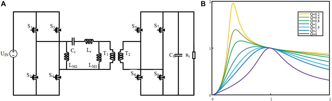
FIGURE 1. (A) Traditional bidirectional LLC model. (B) Gain curve of traditional topology.
Many problems are faced in the traditional model, especially at the light load condition, where the output voltage is limited by its character. The voltage is higher than the reference, which is settled in advance. When the frequency increases to a certain value, the voltage increases instead, which is inconsistent with the obtained gain curve. Therefore, a new model has been established so that the traditional model runs counter to the reality under the light load condition.
2.2 The model with parasitic capacitance
The parasitic capacitance of the transformer is considered in this new model, which is more realistic than the traditional model. The transformer has two windings and stray capacitances, C1 and C2, which are the self-capacitances of the transformer. C0 is the mutual capacitance between the primary and secondary sides. Generally, the parasitic resistances of windings are ignored due to the value being too small, as shown in Figure 2A. The secondary side is converted to the primary side, where the stray capacitances are expressed as in Eq. 1, and the windings are replaced by the inductance and magnetic core in Figure 2B. The stray capacitance can be simplified as in Eq. 2 which is calculated by the two-port net approach (Lu et al., 2003) since the effort of Cs0 is insignificant. The SR junction capacitance is included in this model, and the parasitic capacitance can finally be described by Eq. 3. The capacitance circled in red is equivalent to the resulting parasitic capacitance in Figure 2D.
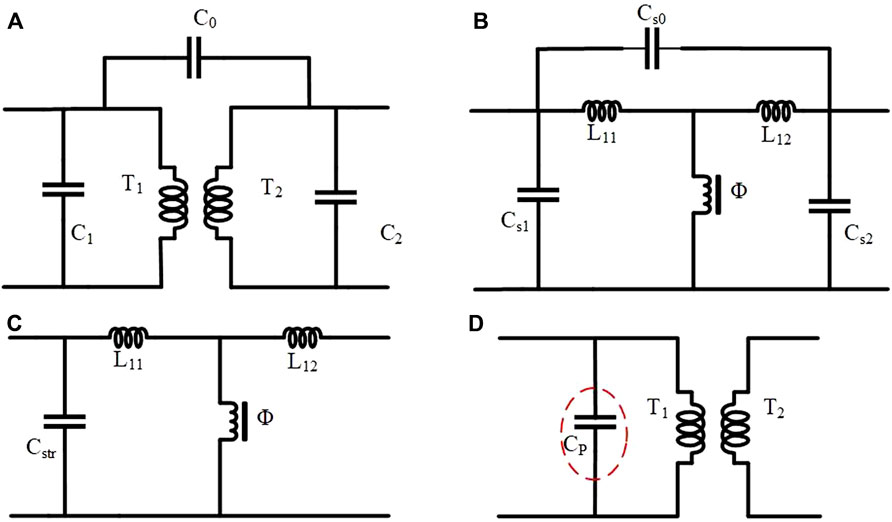
FIGURE 2. (A–D) The model considering parasitic capacitance.
Some things are known before analyzing the LLC converter. The switching model is idealized without loss. In addition, the parasitic capacitance is placed in front of the transformer. Voltage commutation and current commutation exist in every cycle, in which the first half and the second half of the cycle are the same. Hence, only the half-cycle has been described based on the PI controller under the light load condition in the following.
Mode1 (t0-t1): S1 and S4 are turned on and S2 and S3 are turned off. At this period, Lr and Cp are in resonance owing to the value of the magnetic inductors being higher than the resonant inductor and the Cp being higher than the Cr. Therefore, the voltage of the resonance cavity is approximately zero, and the current increases gradually as shown in Figure 3A.
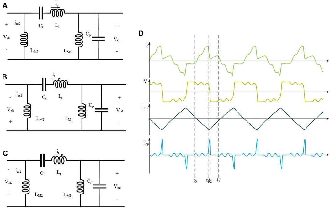
FIGURE 3. (A–C) Mode analysis and (D) waveforms of the circuit in full-bridge.
Mode2 (t1-t2): All switches are all off in this period as shown in Figure 3B. The voltage changes its direction, and voltage Vab is reversed. The Lr and CP keep resonance until the resonance current equals the magnetic current, as shown in Figure 3D.
Mode3 (t2-t3): The resonance current is smaller than the magnetic current. Therefore, the voltage drop is limited by the secondary side. In this period, the resonance cavity has been in resonance where Cr and Lr occur, and there is no other resonance. This mode lasts when the current in LM2 equals to the current in the resonator. The current reversal ends when this mode ends, and the second half period is the same due to the symmetric structure.
FHA is adopted for analyzing this model, which only leaves the fundamental component as the object of the study. The circuit, as shown in Figure 4, can be simplified, in which Vab is the voltage at the midpoint of the two bridge arms and Req is converting the actual load to the original side. The relationship between the input voltage and Vab is described as in Eq. 4, and the same can be the relationship between the output voltage and Vcd (Eq. 5).
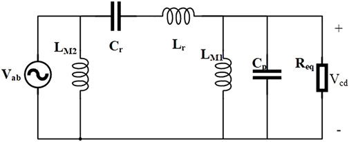
FIGURE 4. The simplified model considering the parasitic capacitance.
The voltage gain shown in Eq. 6 can be obtained by substituting the formula and simplifying it based on the voltage partition principle.
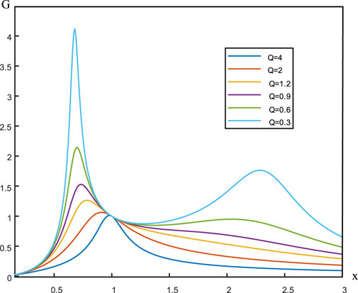
FIGURE 5. Gain curve when Q is fixed.
3 The control method for the model considering the parasitic capacitance
The control method for the new model considering the parasitic capacitance is proposed to solve the problem under the light load condition, which includes two modes: half-bridge (HB) mode and full-bridge (FB) mode. This proposed control method is applied for widening the output range and is kept constant under the light load condition. According to Figure 5, the boundary between the light and heavy load can be calculated. Taking the derivative of the gain, Eq. 8 can be obtained.
The curve with two spikes can be denoted as the light load, and the parameters are substituted into Eq. 9. The light and heavy loads are divided by Eq. 9. Req, which is the equivalent resistance of the secondary side (10), belongs to the pure resistance load, as expressed by Eq. 10, which can be regarded as under the light load condition caused by the load being very small. After sampling the output voltage and current, the calculated resistance is substituted into Eq. 9. When the equation is greater than zero, the load is deemed as the light one. When the frequency is at the left of the switching point, a traditional PI controller mentioned previously is adopted under light load conditions. At this period, the topology is in the FB mode, in which S3 and S4 keep in sync with S2 and S1. The topology becomes HB mode when the switching frequency is higher than the switching point.
S3 keeps off normally, while S4 keeps on in the HB mode, as shown in Figure 6A. The first bridge arm has maintained 50% duty approximately and remained complementary, and the frequency of switches is controlled according to the gain curve shown in Figure 6B. Vab becomes half in the FB mode. The secondary side switches are consistent with the primary side in frequency as a synchronous rectification scheme. The working state of the resonator in the HB mode is the same as that in the FB mode, in which the parasitic capacitance and resonance are in resonance before current commutation.
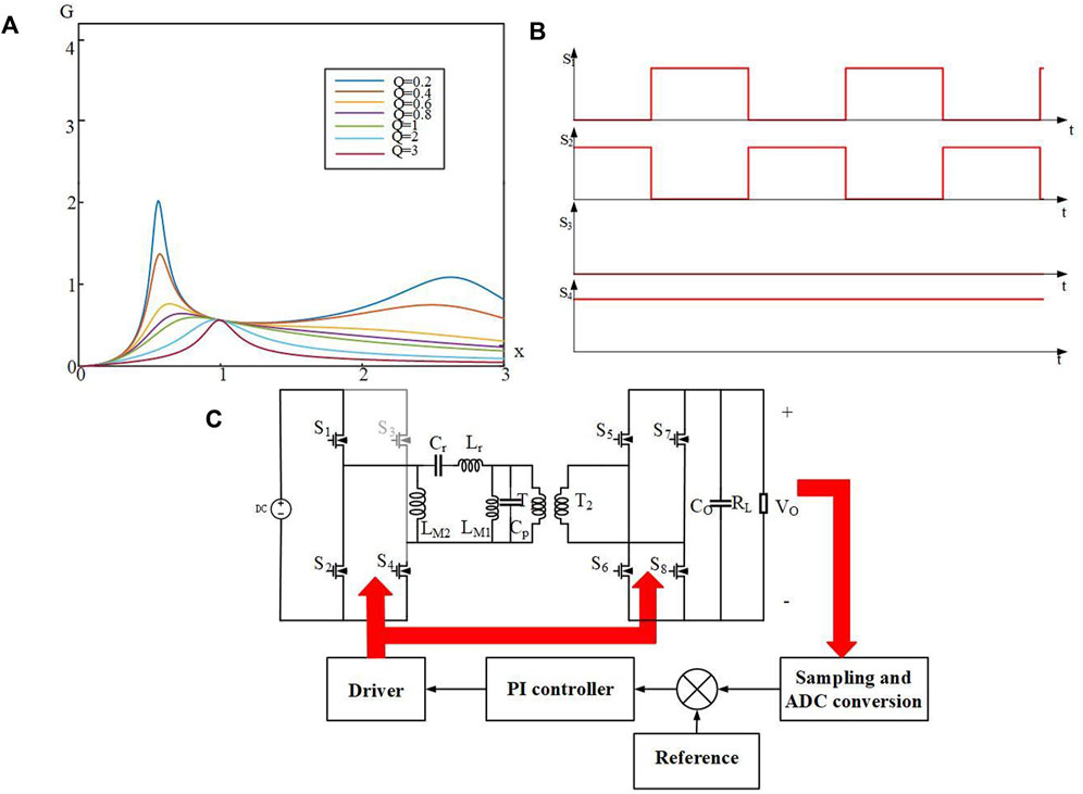
FIGURE 6. (A) The gain curve in the HB mode; (B) the driver signal in the HB mode, and (C) the LLC converter circuit structure.
When switching the modes, the output voltage is kept constant without a giant ripple so that the ratio of the voltage and frequency tends to be zero. The ratio is equal to the value of the derivative approximately. In the heavy load, Eq. 8 has only one solution greater than zero, which is the minimum switching frequency. The maximum switching frequency related to the gain range of the output is artificially limited and is defined as fP2. If the output voltage is required to be large, the value of fp2 is high, while if the output voltage is required to be small, the value of the fp2 is low, as shown in Figure 7A. The switching frequency fs is greater than fp1 at the heavy load when the switching frequency increases and the output voltage decreases.
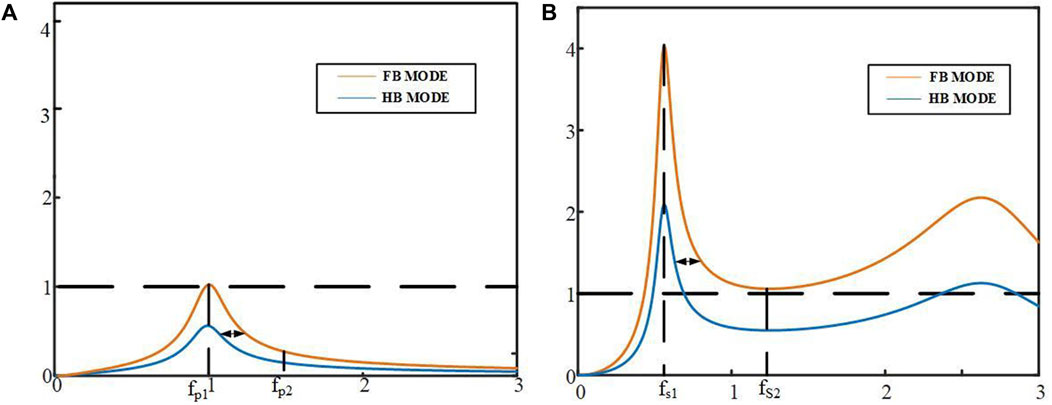
FIGURE 7. (A) Switching topology in the heavy load. (B) Switching topology under the light load.
When Eq. 8 equals zero under the light load, two of the solutions are chosen as the switching point, named fs1 and fs2, respectively, as shown in Figure 7B. Due to the parameters in this circuit, there are three possible values of fs2, greater than 1, less than 1, and equal to 1. It is of no sense to discuss the solutions that fs2 is less than or equal to 1 due to the reason of the extreme parameter values. The solution of fs2 greater than one is discussed as follows. Under the light load, the switching frequency, fs, is greater than fs1 and less than fs2, and the output voltage decreases with the increase of switching frequency. When the switching frequency is greater than fs2, the output voltage increases with the increase in the switching frequency. Also, the switching points in the half-bridge mode and full-bridge mode are the same.
In the HB mode, the switching frequency decreases when the load increases. When the frequencies of S1 and S2 decline to fp1 or fs1 and the output is still less than the reference value, the mode is switched to the FB mode and the frequencies of S1 and S2 keep varying. In the FB mode, the load decreases and the switching frequency increases. When the switching frequency increases to fp2 or fs2 and the reference value is less than the output voltage, the mode is switched to the HB mode.
Suppose the signals of S3 and S4 vary in one period after arriving at the switching point, then the inductors lose the volt-second balance, and the components may be penetrated after reaching saturation due to the tremendous impact caused by topology mutation. Since the controller has a slow signal corresponding to this circuit, the switching time is extended to reduce the influence caused by topology change.
The duty cycle changes in the process of mode switching. The S3 duty cycle changes from 0 to 50%, and the S4 duty cycle changes from 100 to 50%. Mode switching is implemented in several cycles to prevent voltage spikes and current spikes in the changing process. In the variation, S1 and S4 end simultaneously in one cycle, while S2 and S3 end simultaneously, which is kept complementary to ensure that the circuit is running correctly, as shown in Figure 8. During transition, the switching frequencies of S1 and S2 continue to be regulated by the PI controller. The switching frequencies of S1 and S2 are adjusted without considering the duty cycle changes of S3 and S4 for maintaining the output constant. The switching frequency of the first arm bridge decreases with the increasing load and increases with the decreasing load. The overall control process is shown in Figure 9.
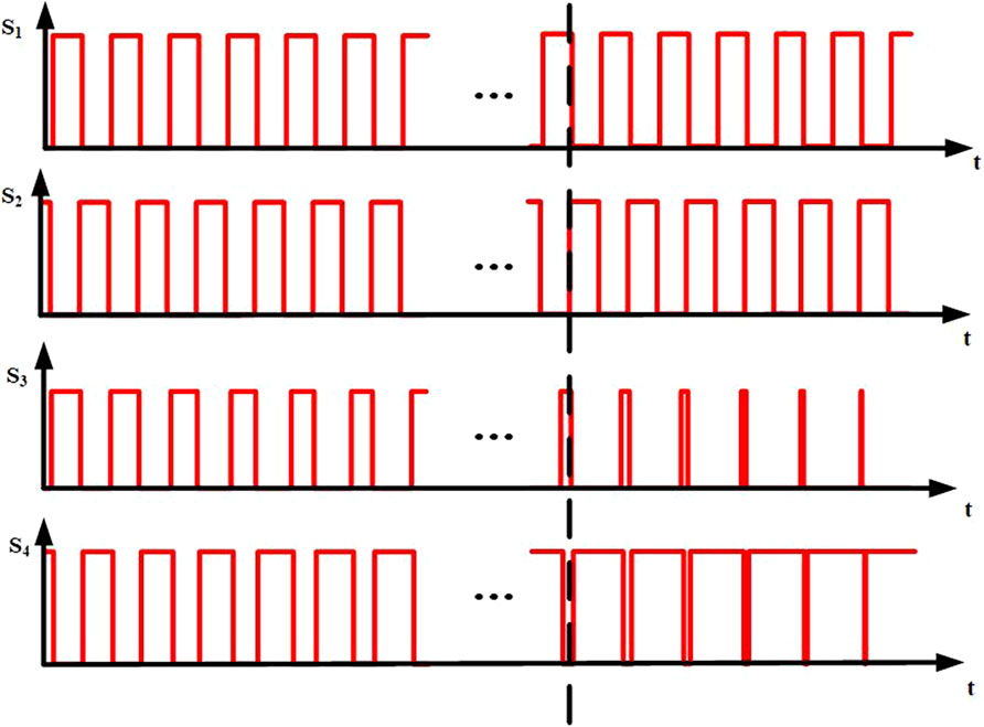
FIGURE 8. Drive signal during transition.
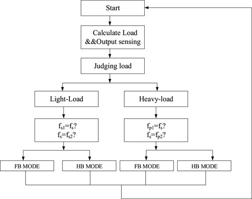
FIGURE 9. Control process.
4 The experiment
The prototype is connected to an energy storage device at one end and a smart grid at the other, as shown in Figure 10. The input voltage is limited from 360 V to 440 V, and the output voltage is kept constant at 36 V. The maximum output current in the forwarding mode equals 27 A, and 2.5 A in the reversed mode, whereas the maximum power is 1 kW. The resonance frequency is set as 100 k, the same as the switching frequency in the full load in theory. Due to the components having parasitic parameters, the actual resonant frequency has some differences from the theoretical one. Considering the current and voltage stress, the components have 2–3 times margin. The digital control can be more flexible in various situations compared with the analog control, with the computing power and speed required for existing integrated chips. In this prototype, DSP, TMS320F28335 (Tohid et al., 2018) published by Texas Instruments as the digital controller, plays a role that occurs in the driving signal, performing the digital to analog conversion, sampling unit, and so on. The switching frequency is calculated. The output current and voltage, which are sampled by the Hall element, are converted to a digital form by the analog to a digital converter in DSP. The main converter parameters are shown in Table 1. It is worth mentioning that the prototype is only for principle verification, so the power density is not considered in the design.
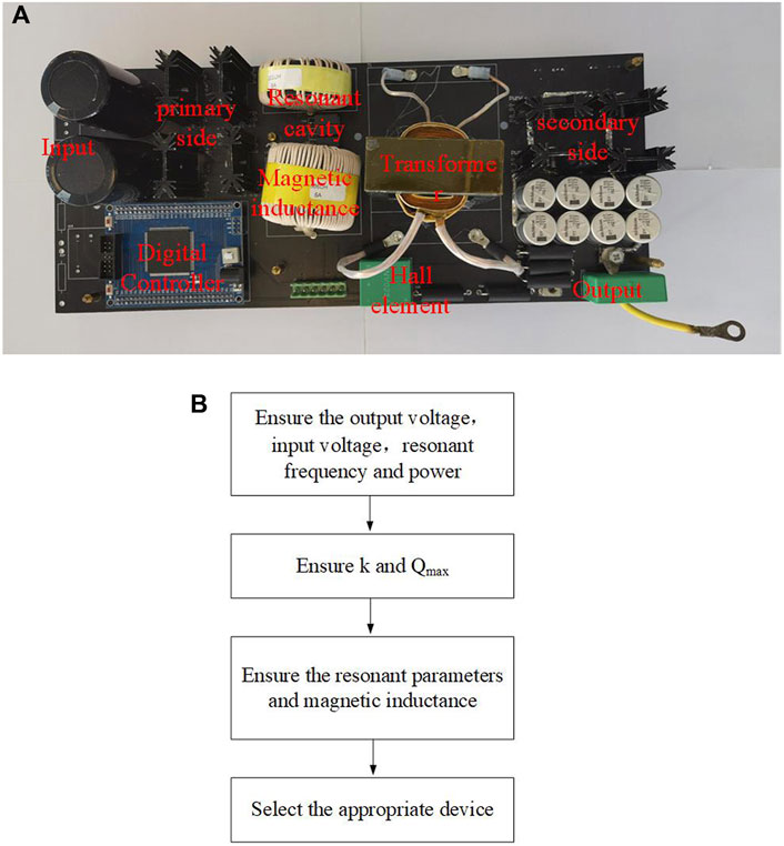
FIGURE 10. (A) The prototype. (B) The parameter calculation procedure.

TABLE 1. Detailed parameters in the prototype.
Figure 11A shows the waves, including the H-bridge voltage and the resonant current. The voltage is around 400 V in the HB mode, where S3 keeps 0% and S4 keeps 100% duty. Figure 11B shows the H-bridge voltage and current in the FB mode, where S3 and S4 keep 50% duty. The voltage varies from +400 V to −400 V. The modes are switched due to the input voltage and load variable.
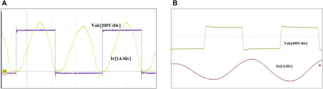
FIGURE 11. (A) Waveforms in the HB mode and (B) waveforms in the FB mode.
In Figure 12, the load is constant and the reference value is changed. Figure 12A shows the oscilloscope waveform, and Figures 12B-D show the waveforms displayed by the host computer. Point B, point C, and point D are simultaneous and the reference voltage changes from 36 V to 48 V. The reference value increases, the mode switches to full bridge mode, and the frequency drops. Point A indicates that the reference value changes from 48 V to 36 V. The reference value drops, switching from the FB mode to the HB mode. The mode is switched when the reference has been changed, and the output range is widened.
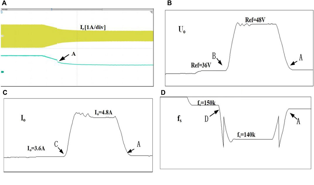
FIGURE 12. Reference change: (A) Graph of an oscilloscope. (B–D) The waveform monitored by the upper computer.
In Figure 13, the reference value is constant at 36 V and the load is changed. Figures 13A, B show the waveforms on the oscilloscope and Figures 13C–E show the waveforms on the host computer. At point A, the load decreases, the current decreases, and the converter is handed over from the FB mode to the HB mode. At point B, the load increases and the converter is handed over from the FB mode to the HB mode. When the load changes, the output voltage transitions smoothly and can maintain the constant voltage under a light load. Although controlled by PI, the reaction speed is faster. A green wave indicates the voltage of the H-bridge, a red wave indicates the current of the resonator, and the black wave indicates the output voltage. At the C point, the load is decreased but the reference is kept constant. There is only switching frequency controlled by PI in the traditional control method.
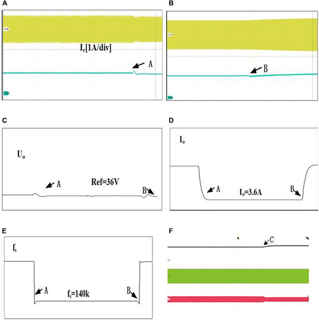
FIGURE 13. Load change. (A,B) Graph of oscilloscope (C–E) waveform monitored by the upper computer. (F) Output waves without considering the parasitic capacitance.
Compared with the conventional method, S1 and S2 are complementary conduction according to 50% duty cycle in the proposed method of the light load. S3 is kept always on and S4 is kept always off. Therefore, S3 and S4 have lower switching losses. Therefore, the efficiency is improved compared with the traditional method in the light load. The proposed control method is the same as the conventional method, and hence, the efficiency is the same. In Figure 14, the horizontal axis represents the load and the vertical axis represents efficiency. As the load increases, the efficiency gradually increases. The efficiency is the highest when the load reaches 80%, after which the efficiency decreases with the load. The loss can be divided into two types, the fixed loss and the variable loss. The fixed loss includes the transformer loss, the switching loss, and the line loss. Under the light load, the fixed loss accounts for a larger proportion, so the efficiency is low. As the load increases, the proportion of the fixed loss becomes smaller and smaller, with the highest efficiency at about 80% load. With the increase of load, the current increases, the heat loss increases, and the efficiency decreases.
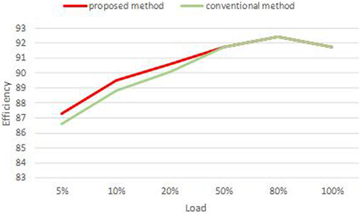
FIGURE 14. Efficiency comparison.
5 Conclusion
The control method is based on the new model considering parasitic capacitance, which plays a vital role in adjusting the output voltage and broadening the output range. In this paper, the model considering parasitic capacitance is more realistic than before, in which the gain curve has two spikes. In addition, the definition of the light load is given on the basis of the gain. Also, the switching frequency, which varies under different load conditions, has been adjusted depending on the gain curve by the PI controller, and there are two modes in this control: the HB mode and the FB mode. The output can be maintained constant under light load conditions and can be widened. The variation of the driving signal is also given to avoid topological mutation causing damage to other devices in transition. It is proven that the model and control method presented in this paper is effective in a 400V-36V-1 kW prototype. Compared with the previous methods, it can improve the efficiency and ensure the constant output voltage under the light load (Wang et al., 2022c).
Data availability statement
The original contributions presented in the study are included in the article/Supplementary Material. Further inquiries can be directed to the corresponding author.
Author contributions
All authors listed have made a substantial, direct, and intellectual contribution to the work and approved it for publication.
Funding
This research was funded by the Fundamental Research Funds for the Central Universities grant number N2204007.
Conflict of interest
QA was employed by Changguang Satellite Technology Co., Ltd.
The remaining authors declare that the research was conducted in the absence of any commercial or financial relationships that could be construed as a potential conflict of interest.
Publisher’s note
All claims expressed in this article are solely those of the authors and do not necessarily represent those of their affiliated organizations, or those of the publisher, the editors, and the reviewers. Any product that may be evaluated in this article, or claim that may be made by its manufacturer, is not guaranteed or endorsed by the publisher.
References
Ahmed, M. H., Fei, C., Lee, F. C., and Li, Q. (2017). 48-v voltage regulator module with PCB Winding Matrix Transformer for future data centers. IEEE Trans. Ind. Electron. 64 (12), 9302–9310. doi:10.1109/TIE.2017.2711519
Awasthi, A., Bagawade, S., and Jain, P. K. (2021). Analysis of a hybrid variable-frequency-duty-cycle-modulated low-Q LLC resonant converter for improving the light-load efficiency for a wide input voltage range. IEEE Trans. Power Electron. 36 (7), 8476–8493. doi:10.1109/TPEL.2020.3046560
Fei, C., Ahmed, M. H., Lee, F. C., and Li, Q. (2017). Two-stage 48v-12v/6v-1.8v voltage regulator module with dynamic bus voltage control for light-load efficiency improvement. IEEE Trans. Power Electron. 32 (7), 5628–5636. doi:10.1109/TPEL.2016.2605579
Feng, W., Huang, D., Mattavelli, P., Fu, D., and Lee, F. C. (2010). “Digital implementation of driving scheme for synchronous rectification in llc resonant converter,” in 2010 IEEE Energy Conversion Congress and Exposition, Atlanta, GA, USA, 12-16 September 2010.
Feng, W., Mattavelli, P., and Lee, F. C. (2013). Pulsewidth locked loop (PWLL) for automatic resonant frequency tracking in LLC DC–DC transformer (LLC -dcx). IEEE Trans. Power Electron. 28 (4), 1862–1869. doi:10.1109/TPEL.2012.2210912
Hou, N., Song, W., Li, Y., Zhu, Y., and Zhu, Y. (2019). A comprehensive optimization control of dual-active-bridge dc–dc converters based on unified-phase-shift and power-balancing scheme. IEEE Trans. Power Electron. 34, 826–839. doi:10.1109/TPEL.2018.2813995
Hu, X., Zhang, H., Ma, D., and Wang, R. (2022). Hierarchical pressure data recovery for pipeline network via generative adversarial networks. IEEE Trans. Autom. Sci. Eng. 19 (3), 1960–1970. doi:10.1109/TASE.2021.3069003
Hu, X., Zhang, H., Ma, D., Wang, R., and Tu, P. (2022). Small leak location for intelligent pipeline system via action-dependent heuristic dynamic programming. IEEE Trans. Ind. Electron. 69, 11723–11732. doi:10.1109/TIE.2021.3127016
Hu, Z., Qiu, Y., Wang, L., and Liu, Y. (2014). An interleaved LLC resonant converter operating at constant switching frequency. IEEE Trans. Power Electron. 29 (6), 2931–2943. doi:10.1109/TPEL.2013.2273939
Huang, J., Wang, Y., Li, Z., and Lei, W. (2016). Unified triple-phase-shift control to minimize current stress and achieve full soft-switching of isolated bidirectional dc–dc converter. IEEE Trans. Ind. Electron. 63, 4169–4179. doi:10.1109/TIE.2016.2543182
Jeung, Y., and Lee, D. (2019). Voltage and current regulations of bidirectional isolated dual-active-bridge dc–dc converters based on a double-integral sliding mode control. IEEE Trans. Power Electron. 34, 6937–6946. doi:10.1109/TPEL.2018.2873834
Jiang, T., Zhang, J., Wu, X., Sheng, K., and Wang, Y. (2015). A bidirectional LLC resonant converter with automatic forward and backward mode transition. IEEE Trans. Power Electron. 30 (2), 757–770. doi:10.1109/TPEL.2014.2307329
Jiang, T., Zhang, J., Wu, X., Sheng, K., and Wang, Y. (2016). A bidirectional three-level LLC Resonant converter with PWAM control. IEEE Trans. Power Electron. 31 (3), 2213–2225. doi:10.1109/TPEL.2015.2438072
Jung, J., Kim, H., Ryu, M., and Baek, J. (2013). Design methodology of bidirectional CLLC resonant converter for high-frequency isolation of DC distribution systems. IEEE Trans. Power Electron. 28 (4), 1741–1755. doi:10.1109/TPEL.2012.2213346
Kang, S., and Cho, B. (2017). Digitally implemented charge control for llc resonant converters. IEEE Trans. Ind. Electron. 64 (8), 6159–6168. doi:10.1109/TIE.2017.2682801
Kundu, U., Yenduri, K., and Sensarma, P. (2017). Accurate zvs analysis for magnetic design and efficiency improvement of full-bridge llc resonant converter. IEEE Trans. Power Electron. 32 (3), 1703–1706. doi:10.1109/TPEL.2016.2604118
Lee, I., and Moon, G. (2014). The K-Q analysis for an LLC series resonant converter. IEEE Trans. Power Electron. 29 (1), 13–16. doi:10.1109/TPEL.2013.2255106
Lee, J., Kim, J., Kim, J., Baek, J., and Moon, G. (2015). A High-efficiency PFM half-bridge converter utilizing a half-bridge LLC converter under light load conditions. IEEE Trans. Power Electron. 30 (9), 4931–4942. doi:10.1109/TPEL.2014.2365625
Li, H., Wang, S., Zhang, Z., Zhang, J., Zhu, W., Ren, X., et al. (2022). A bidirectional synchronous/asynchronous rectifier control for wide battery voltage range in sic bidirectional llc chargers. IEEE Trans. Power Electron. 37 (5), 6090–6101. doi:10.1109/TPEL.2021.3126886
Li, H., Wang, S., Zhang, Z., Zhang, J., Zhu, W., Ren, X., et al. (2022). An impedance-based digital synchronous rectifier driving scheme for bidirectional high-voltage sic llc converter. IEEE Trans. Ind. Electron. 69 (11), 11314–11323. doi:10.1109/TIE.2021.3127037
Li, H., Zhang, Z., Wang, S., Tang, J., Ren, X., and Chen, Q. (2020). A 300-kHz 6.6-kW sic bidirectional LLC onboard charger. IEEE Trans. Ind. Electron. 67 (2), 1435–1445. doi:10.1109/TIE.2019.2910048
Liao, Y., Xu, G., Sun, Y., Peng, T., Su, M., Guo, B., et al. (2021). Single-stage DAB-LLC hybrid bidirectional converter with tight voltage regulation under DCX operation. IEEE Trans. Ind. Electron. 68, 293–303. doi:10.1109/TIE.2020.2965495
Liu, C., Liu, H., Cai, G., Cui, S., Liu, H., and Yao, H. (2017). Novel hybrid LLC resonant and DAB linear DC-DC converter: Average model and experimental verification. IEEE Trans. Ind. Electron. 64 (9), 6970–6978. doi:10.1109/TIE.2017.2682784
Lu, H. Y., Zhu, J. G., and Hui, S. Y. R. (2003). Experimental determination of stray capacitances in high frequency transformers. IEEE Trans. Power Electron. 18 (5), 1105–1112. doi:10.1109/TPEL.2003.816186
Lu, Y., Wu, Q., Wang, Q., Liu, D., and Xiao, L. (2018). Analysis of a novel zero-voltage-switching bidirectional dc/dc converter for energy storage system. IEEE Trans. Power Electron. 33, 3169–3179. doi:10.1109/TPEL.2017.2703949
Ma, D., Cao, X., Sun, C., Wang, R., Sun, Q., Xie, X., et al. (2022). Dual-predictive control with adaptive error correction strategy for AC microgrids. IEEE Trans. Power Deliv. 37 (3), 1930–1940. doi:10.1109/TPWRD.2021.3101198
Song, W., Hou, N., and Wu, M. (2018). Virtual direct power control scheme of dual active bridge dc–dc converters for fast dynamic response. IEEE Trans. Power Electron. 33, 1750–1759. doi:10.1109/TPEL.2017.2682982
Tohid, R., Wagle, B., Shirzad, S., Diehl, P., Serio, A., Kheirkhahan, A., et al. (2018). Asynchronous execution of Python code on task-based runtime systems. Ithaca: IEEE, 37–45.
Wang, K., Wei, G., Wei, J., Wu, J., Wang, L., and Yang, X. (2022a). Current detection and control of synchronous rectifier in high-frequency LLC Resonant Converter. IEEE Trans. Power Electron. 37 (4), 3691–3696. doi:10.1109/TPEL.2021.3119770
Wang, R., Jiang, S., Ma, D., Sun, Q., Zhang, H., and Wang, P. (2022b). The Energy Management of multi-port energy router in smart home. IEEE Trans. Consum. Electron. 1, 1. doi:10.1109/TCE.2022.3200931
Wang, R., Li, W., Sun, Q., Li, Y., Gui, Y., and Wang, P. (2022c). Fully distributed dynamic edge-event-triggered current sharing control strategy for multi-bus dc microgrids with power coupling. IEEE Trans. Ind. Inf. 2022, 1–11. doi:10.1109/TII.2022.3188352
Xue, B., Wang, H., Liang, J., Cao, Q., and Li, Z. (2021). Phase-shift modulated interleavedllc converter with ultrawide output voltage range. IEEE Trans. Power Electron. 36 (1), 493–503. doi:10.1109/TPEL.2020.3001126
Yoon, H., Lee, H., Ham, S., Choe, H., and Kang, B. (2018). Off-time control of <italic>LLC</italic> resonant half-bridge converter to prevent audible noise generation under a light-load condition. IEEE Trans. Power Electron. 33 (10), 8808–8817. doi:10.1109/TPEL.2017.2774840
Keywords: DC-DC converter, half bridge, full bridge, digital control, topological changes
Citation: Han Y, Ma D and An Q (2023) A switching control method based on a new model considering parasitic capacitance for LLC. Front. Energy Res. 10:1052004. doi: 10.3389/fenrg.2022.1052004
Received: 23 September 2022; Accepted: 31 October 2022;
Published: 13 January 2023.
Edited by:
Jingyang Fang, Shandong University, ChinaReviewed by:
Bin Duan, Shandong University, ChinaTohid Rahimi, Carleton University, Canada
Dehao Qin, Clemson University, United States
Copyright © 2023 Han, Ma and An. This is an open-access article distributed under the terms of the Creative Commons Attribution License (CC BY). The use, distribution or reproduction in other forums is permitted, provided the original author(s) and the copyright owner(s) are credited and that the original publication in this journal is cited, in accordance with accepted academic practice. No use, distribution or reproduction is permitted which does not comply with these terms.
*Correspondence: Yetong Han, MjAwMDY2NUBzdHUubmV1LmVkdS5jbg==