- School of Electric Power Engineering, Nanjing Institute of Technology, Nanjing, China
Voltages sags have become the major issue that prevents the customers from getting high-quality power supply, and the dynamic voltage restorer (DVR) is considered an effective way to solve this issue. In this work, a method for voltage sag detection implemented in the time-domain is firstly addressed, which features highly accurate and fast response. Then, the dual-loop voltage–current control for the DVR is intensively investigated. Specifically, the optimal tuning of the inner current loop to achieve the maximum active damping is approached, and the voltage controller implemented in the discrete-time is developed. Tuning of the voltage loop based on critical damping is also approached, which features reduced settling time and avoidance of overshoot. The simulation and experimental results have verified the effectiveness of the proposed method for detection and management of voltage sags.
1 Introduction
It has been reported that according to the statistics, voltage sags, which can cause enormous economic loss every year, account for over 70% of the cases that give rise to the power-supply deterioration, resulting in severe complaints from the customers (Nagata et al., 2017; Parreño Torres et al., 2019; Han et al., 2020). In other words, voltage sags have become the major issue that prevents consumers from getting the uninterrupted and high-quality power supply.
Many literature studies have been devoted to the control and management of voltage sags for a long period of time (Jowder, 2009; Nagata et al., 2017; Parreño Torres et al., 2019; Gontijo et al., 2020; Han et al., 2020). Presently, among the proposed methods, the dynamic voltage restorer (DVR), which is connected between the grid and the load, has been commonly considered an effective and economical way to solve the issue of voltage sags, and a high-quality power supply can be expected. The basic idea of DVR is to generate the compensation voltage through the power-electronics–based converter, so as to keep the load-side voltage unaffected when sags occur on the grid-side voltage. Consequently, the fast and accurate voltage sag detection and the effective voltage regulation strategy are of almost importance to the DVR to achieve a high level of performance.
With regard to sag detection, many methods have been developed from either the time- or frequency-domain, such as the Kalman filter (Cisneros-Magaña et al., 2018), fast Fourier transform (Wang Y et al., 2019), wavelet transform (Hu et al., 2020), and approaches based on instantaneous reactive power theory (Pradhan and Mishra, 2019; Tu et al., 2020; He et al., 2021). Specifically, it has been proved that both the output speed and the accuracy of the Kalman filter are related to the system model, and there is also convergence issue which can result in an unstable response. Alternatively, methods based on the Fourier or wavelet transforms require historical data, resulting in heavy computation burden which is, therefore, unacceptable for real-time signal implementation with a commercial digital signal processor (DSP) or microcontroller unit (MCU). Although this issue can be avoided with the employment of a sliding window as addressed by Wang J et al. (2019), it has, however, been proved that there are also stability and high-frequency noise amplification issues, which need careful considerations for the practical implementation with a DSP or MCU. The method based on instantaneous reactive power theory is suitable for a three-phase system and has, in fact, been studied and implemented in a lot of literature studies, such as He et al. (2021) and Pradhan and Mishra (2019). This kind of method, however, has a blind zone for the detection of unbalanced voltage drops.
On the contrary, for the DVR, the LC filter is commonly employed at the output terminal of the converter. This can put a great challenge to the system’s overall control since the LC filter has resonance phenomenon and causes stability problem (Wang J et al., 2019; Naidu et al., 2019; Bajaj, 2020; Xiong et al., 2020). Although various passive methods, for instance, connecting resisters in parallel or series with the capacitor, have been developed and can be employed to increase the system’s physical damping, this kind of method is however not preferred, since it can further cause other issues, such as increase in power loss and deteriorated filter effectiveness for high-frequency voltage harmonics (Pal and Gupta, 2020; Vo Tien et al., 2018). On the contrary, the counterpart, i.e., active damping methods, is realized by modifying the control structure, which can avoid the aforementioned issues faced by the passive methods, and has therefore been intensively investigated in recent years (Suppioni et al., 2017; Liu et al., 2018; Roldán-Pérez et al., 2019; Liu et al., 2021; Xiong et al., 2021). Specifically, the following two types of control strategies: 1) single-loop voltage and 2) dual-loop voltage–current control, can be employed to achieve enhanced active damping. Nevertheless, it has been addressed that the single-loop voltage control method suffers from the issues of poor stability and constrained loop-bandwidth, which can result in an oscillatory and slow transient response of the output voltage. Hence, this approach is not preferred for high-performance applications, although it has the merits of simple structure and easy implementation.
Alternatively, the dual-loop control method, in which additional active damping can be achieved by incorporating the current loop, has been proved to have improved performance compared to that of the single-loop control method. Hence, numerous studies have been dedicated to the analysis and tuning of the current loop. Commonly, the frequency response analysis is employed in these studies, where the bandwidth of the voltage loop is tuned to be one-fifth to one-tenth of that of the current loop, which is a rule of thumb for a common dual- or multi-loop control structure for grid-following converters. This rule is however not applicable for the dual-loop regulated DVR, since the objective of the current loop is to improve damping, instead of signal tracking where bandwidth is concerned. Hence, the explicit guidance for tuning of the current loop needs to be clarified, which is approached in this work. Also, based on the equivalent plant which is damped with the current loop, a voltage controller implemented in the discrete-time domain is developed, which features fast response and avoidance of overshoot.
To do that systematically, the rest of this work is organized as follows: Section 2 begins with the description of the basic principle of DVR succinctly, and then based on signal reconstruction, a method for voltage sag detection in the time-domain is developed, which features low settling time, high accuracy, and frequency adaptive characteristic. The inner current loop is addressed in Section 3, with the objective of obtaining the maximum active damping. The developed discrete voltage controller is addressed in Section 4, in which the tuning of the voltage loop based on optimization of settling time and overshoot is also addressed. The simulation and experimental verifications are presented in Section 5, before concluding the findings in Section 6.
2 Principle of DVR and Voltage Drop Detection
As shown in Figure 1, the load-side voltage VLoad can be expressed as the superposition of the grid-side voltage VGrid and the compensation voltage VDVR, which can be expressed as follows:
In this manner, when a fault occurs in the main grid or adjacent transmission line, the voltage drop can occur on the grid-side voltage VGrid. The DVR detects the voltage sag and injects the compensation voltage VDVR to the grid through the coupling transformer. In this manner, the load-side voltage VLoad remains stable and the voltage supply for the sensitive load is unaffected.
According to the Fourier theory, the periodic grid voltage can be expressed as the sum of different frequency signals, which can be expressed as follows:
where
where
It can be noted that
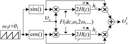
Combining Eqs 2–5, the structure for the detection of the fundamental voltage
From Eqs 4, 5, it can be observed that the frequency of the alternating signals is multiple of the fundamental frequency. Therefore, in this work, a finite impulse response (FIR) filter is employed, whose expression is shown as follows:
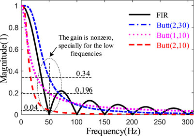
where n is the number of sampling points within a period of the grid voltage. For comparison, the magnitude responses of the FIR filter and Butterworth filter Butt(a, b) are illustrated in Figure 3, noting that a is the order and b is the cutoff frequency of the filter. It can be noted that the amplitude of the FIR filter at the fundamental frequency
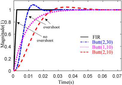
It should be mentioned that the output accuracy of Butt(a, b) can be improved by reducing the cutoff frequency b. This is, however, at the cost of the reduction of the bandwidth for the filter, leading to a slow transient response. As shown in Figure 4 where the step response of different filters is illustrated, comparing Butt(2,30), the settling time is much extended for the case of Butt(1,10) and Butt(2,10). Alternatively, the fastest response can be obtained with the employment of FIR filter, and no overshoot can be observed.
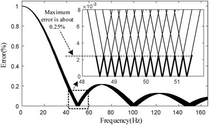
From the above analysis, it can be concluded that, from the viewpoint of accuracy and speed of detection of hx and hy in Eqs 4, 5, the performance of FIR filter is superior to that of Butt(a, b). The main shortcoming of employing the FIR filter (7) is the storage requirement, which is, commonly, RAM for microprocessors. The next step is to achieve frequency adaption for the FIR filter, since the grid voltage
In this manner, with the developed method illustrated in Figure 2, the fundamental grid voltage can finally be obtained, whose amplitude and phase are employed for voltage sag identification. It should be noted that the developed method can be employed for either three- or single-phase configuration, although only the three-phase one is taken as an example for analysis in this work.
3 Optimal Active Damping Tuning of the Inner Current Loop
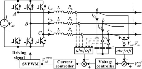
In Figure 6, the main circuit and the corresponding dual-loop control method of the three-phase DVR are both illustrated. The dc bus voltage can be supplied by either a rectifier or an energy storage system. Hence, a dc source Vdc can be assumed for simplicity here. The output of the converter is connected to the LC filter, where L is the inductor, C is the capacitor, and RL is the equivalent resistor which is employed for emulating the power loss of the converter. After the filter, the voltage is fed to the coupling transformer shown in Figure 1. The reference voltage
For better illustration, the dual-loop control method is further depicted in Figure 7, where
The modulation signal
where
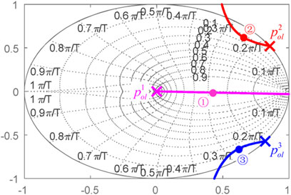
Recalling Figure 7, it can be observed that Eq. 8 is actually the equivalent plant of the voltage controller. Since the inclusion of the current loop is for active damping, the damping characteristic of Eq. 8 is investigated. As shown in Figure 8A, with the increase of K, the conjugate poles
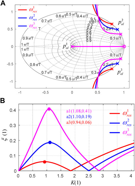
FIGURE 8. Root locus and active damping of the plant when K varies, where (A) shows the root locus and (B) shows the plot of K vs
4 The Development of Voltage Controller in the Discrete-Time Domain
In order to have zero steady-state error signal tracking of the sinusoidal waveform, the following analysis is performed in the synchronous reference frame (SRF). Hence, with the replacement of z with
Observing Figure 9, it can be noted that, with the optimal damping of Kopt, the damping
With the objective of canceling the above weak damping poles, in this work, a voltage controller is developed, whose transfer function is shown as follows:
where
5 Tuning of the Voltage Loop With the Employment of the Developed Controller Based on Critical Damping
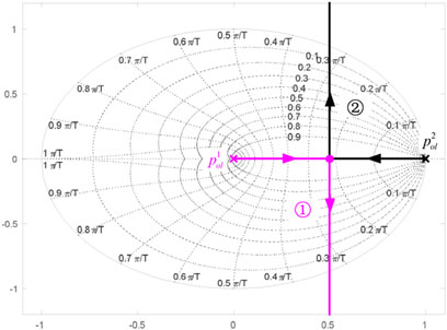
Combining (8), (9), and Figure 7, the open-loop transfer function of the voltage loop can be derived. Then, by varying the controller gain KV from zero to infinity, the root locus of the voltage loop can be obtained, as shown in Figure 10. It can be noted that, for lower values of KV, the closed-loop poles on branches ① and ② are initially on the real axis and move toward the unit circle with the further increase of KV, while for higher values of KV, the poles on both ① and ② can move outside of the circle, resulting in an unstable response of the voltage loop.
Nevertheless, the damping and magnitude of the poles obtained from the discrete root locus analysis are not straightforward as those derived in the continuous-time domain. Hence, the damping and magnitude of the equivalence of the poles in the continuous-time domain are employed for analysis, which can be expressed as follows:
and
where
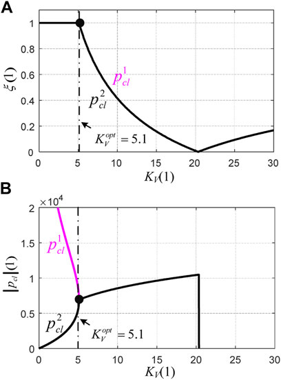
For better illustration, the damping
However, for KV>Kopt V, the magnitude of
Form the above analysis, it can be concluded that, for KV = Kopt V, the possible maximum magnitude of both
6 Simulation and Experimental Results
To verify the effectiveness of the developed method for voltage sag detection and the controller for voltage regulation of DVR, the simulation is performed in Matlab/Simulink. In particular, the parameters are shown as follows: the filter inductance of 0.4 mH, the filter capacitor of 180 uF, the switching frequency of i5 kHz, the sampling frequency of 10 kHz, and the grid line voltage of 380 V.
In Figure 12, the simulation results for the single-phase, dual-phase, and three-phase voltage sags of 40% are illustrated, where the grid-side voltage, the load-side voltage, and the DVR voltage are represented as VGrid, VLoad, and VDVR, respectively. It can be noted that, for the three evaluated cases, the DVR can generate the required voltage within 2 ms approximately, and no overshoot can be observed. In this manner, the load-side voltage remains unaffected and a high-quality power supply can be guaranteed.
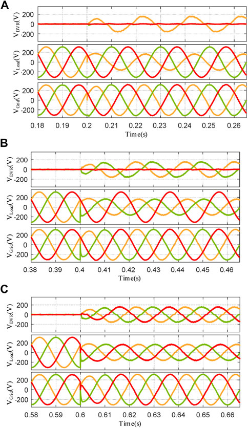
FIGURE 12. Simulation results of (A) single-phase, (B) dual-phase, and (C) three-phase voltage sag compensation for the DVR.
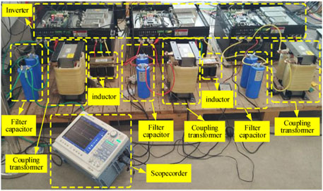
The experimental setup is shown in Figure 13, whose parameters are the same as those addressed for simulation. The rated capacity of the setup is 100 kVA. The digital controller is a TMS320F28346 DSP and a EP3C25 FPGA, and the DSP is responsible for the calculation and data process, while the FPGA is employed for logic management and protection. Also, the measuring equipment includes a DL850 ScopeCorder and several P5200 differential probes.
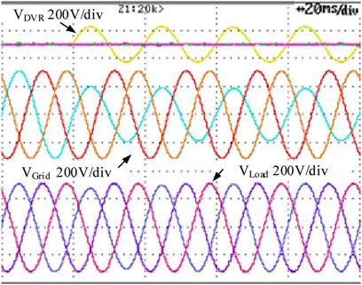
The experiment is performed for different voltage sag sceneries. To begin with, the single-phase voltage sag of 40% is investigated. As shown in Figure 14, it can be noted that the DVR compensation voltage has a fast response with no overshoot, which is in good agreement with the theoretical findings addressed before. In this manner, the load-side voltage is stable regardless of the sag on the grid-side voltage.
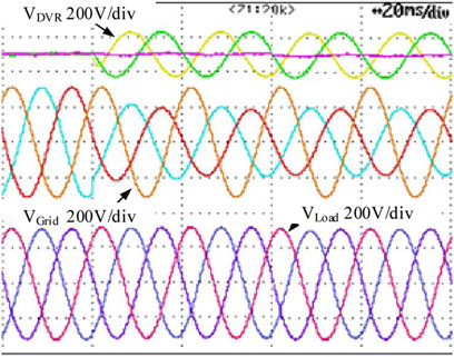
Also, the case of dual-phase voltage sag of 40% is addressed. The experimental result is shown in Figure 15, where it can be observed the settling time is about 2 ms with no overshoot, which agrees with the analytical findings addressed before.
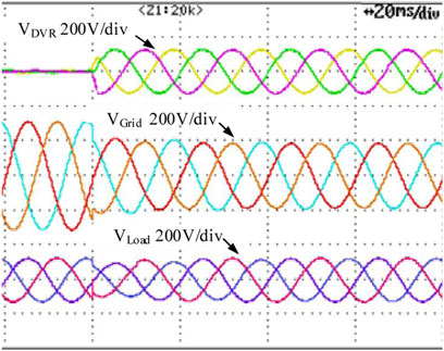
Finally, the case of voltage sag for the three-phase voltage is investigated. As shown in Figure 16, the amplitude of the three-phase voltage sag is 40% simultaneously, and the compensation voltage is fast and accurate, and a similar conclusion to that of the single- and dual-phase voltage drops can be drawn, i.e., reduced settling time and avoidance of overshoot. It should be emphasized that if non-linear loads are considered, the load-side voltage can be distorted by the high-frequency harmonic currents, since the voltage controller developed in this work is employed for handling the fundamental frequency voltage.
7 Conclusion
In this work, the DVR for voltage sag compensation is intensively addressed. A method implemented in the time-domain for voltage sag identification is developed, which features fast response, high accuracy, and frequency adaptive characteristic. Then, the dual-loop voltage–current regulation for the DVR is approached, where the optimal tuning of the current loop to achieve the maximum active damping is addressed. Also, a discrete voltage controller is developed, and tuning of the voltage loop based on critical damping is lastly addressed, which can be employed to achieve a fast response and avoidance of overshoot for output voltage regulation.
Data Availability Statement
The original contributions presented in the study are included in the article/supplementary material, and further inquiries can be directed to the corresponding author.
Author Contributions
All authors listed have made a substantial, direct, and intellectual contribution to the work and approved it for publication.
Funding
This work was supported by the National Natural Science Foundation of China (No. 51807092), Open Fund of Jiangsu Distribution Network Intelligent Technology and Equipment Collaborative Innovation Center (XTCX202004, XTCX201905), and Hubei Provincial Key Laboratory for Operation and Control of Cascaded Hydropower Station (2019KJX04).
Conflict of Interest
The authors declare that the research was conducted in the absence of any commercial or financial relationships that could be construed as a potential conflict of interest.
Publisher’s Note
All claims expressed in this article are solely those of the authors and do not necessarily represent those of their affiliated organizations, or those of the publisher, the editors, and the reviewers. Any product that may be evaluated in this article, or claim that may be made by its manufacturer, is not guaranteed or endorsed by the publisher.
References
Bajaj, M. (2020). Design and Simulation of Hybrid DG System Fed Single-phase Dynamic Voltage Restorer for Smart Grid Application. Smart Sci. 8 (1), 24–38. doi:10.1080/23080477.2020.1748928
Cisneros-Magaña, R., Medina, A., and Anaya-Lara, O. (2018). Time-Domain Voltage Sag State Estimation Based on the Unscented Kalman Filter for Power Systems with Nonlinear Components. Energies 11 (6), 1411. doi:10.3390/en11061411
Gontijo, G. F., Tricarico, T. C., da Silva, L. F., Krejci, D., França, B. W., Aredes, M., et al. (2020). Modeling, Control, and Experimental Verification of a DFIG with a Series-Grid-Side Converter with Voltage Sag, Unbalance, and Distortion Compensation Capabilities. IEEE Trans. Industry Appl. 56 (1), 584–600. doi:10.1109/TIA.2019.2946950
Han, Y., Feng, Y., Yang, P., Xu, L., Xu, Y., and Blaabjerg, F. (2020). Cause, Classification of Voltage Sag, and Voltage Sag Emulators and Applications: A Comprehensive Overview. IEEE Access 8, 1922–1934. doi:10.1109/access.2019.2958965
He, H.-Y., Zhang, W.-H., Wang, Y., and Xiao, X.-Y. (2021). A Sensitive Industrial Process Model for Financial Losses Assessment Due to Voltage Sag and Short Interruptions. IEEE Trans. Power Deliv. 36 (3), 1293–1301. doi:10.1109/tpwrd.2020.3006017
Hu, W. X., Xiao, X. Y., and Zheng, Z. X. (2020). Voltage Sag/swell Waveform Analysis Method Based on Multi‐dimension Characterisation. IET Generation, Transm. Distribution 14 (3), 486–493. doi:10.1049/iet-gtd.2019.1038
Jowder, F. A. L. (2009). Design and Analysis of Dynamic Voltage Restorer for Deep Voltage Sag and Harmonic Compensation. IET generation, Transm. distribution 3 (6), 547–560. doi:10.1049/iet-gtd.2008.0531
Liu, B., Li, Z., Chen, X., Huang, Y., and Liu, X. (2018). Recognition and Vulnerability Analysis of Key Nodes in Power Grid Based on Complex Network Centrality. IEEE Trans. Circuits Syst. 65 (3), 346–350. doi:10.1109/tcsii.2017.2705482
Liu, B., Li, Z., Dong, X., Yu, S. S., Chen, X., Oo, A. M. T., et al. (2021). Impedance Modeling and Controllers Shaping Effect Analysis of PMSG Wind Turbines. IEEE J. Emerg. Sel. Top. Power Electron. 9 (2), 1465–1478. doi:10.1109/jestpe.2020.3014412
Nagata, E. A., Ferreira, D. D., Duque, C. A., and Cequeirab, A. S. (2017). Voltage Sag and Swell Detection and Segmentation Based on Independent Component Analysis. Electric Power Syst. Res. 155, 274–280. doi:10.1016/j.epsr.2017.10.029
Naidu, T. A., Arya, S. R., and Maurya, R. (2019). Multiobjective Dynamic Voltage Restorer with Modified EPLL Control and Optimized PI-Controller Gains. IEEE Trans. Power Electron. 34 (3), 2181–2192. doi:10.1109/tpel.2018.2837009
Pal, R., and Gupta, S. (2020). Topologies and Control Strategies Implicated in Dynamic Voltage Restorer (DVR) for Power Quality Improvement. Iran J. Sci. Technol. Trans. Electr. Eng. 44 (2), 581–603. doi:10.1007/s40998-019-00287-3
Parreño Torres, A., Roncero-Sánchez, P., Vázquez, J., López-Alcolea, F. J., and Molina-Martínez, E. J. (2019). A Discrete-Time Control Method for Fast Transient Voltage-Sag Compensation in DVR. IEEE Access 7, 170564–170577. doi:10.1109/access.2019.2955177
Pradhan, M., and Mishra, M. K. (2019). Dual $P$ - $Q$ Theory Based Energy-Optimized Dynamic Voltage Restorer for Power Quality Improvement in a Distribution System. IEEE Trans. Ind. Electron. 66 (4), 2946–2955. doi:10.1109/tie.2018.2850009
Roldán-Pérez, J., García-Cerrada, A., Ochoa-Giménez, M., and Zamora-Macho, J. L. (2019). Delayed-Signal-Cancellation-Based Sag Detector for a Dynamic Voltage Restorer in Distorted Grids. IEEE Trans. Sust. Energ. 10 (4), 2015–2027. doi:10.1109/tste.2018.2877505
Suppioni, V. P., Grilo, A. P., and Teixeira, J. C. (2017). Improving Network Voltage Unbalance Levels by Controlling DFIG Wind Turbine Using a Dynamic Voltage Restorer. Int. J. Electr. Power Energ. Syst. 96, 185–193. doi:10.1016/j.ijepes.2017.10.002
Tu, C., Guo, Q., Jiang, F., Wang, H., and Shuai, Z. (2020). A Comprehensive Study to Mitigate Voltage Sags and Phase Jumps Using a Dynamic Voltage Restorer. IEEE J. Emerg. Sel. Top. Power Electron. 8 (2), 1490–1502. doi:10.1109/jestpe.2019.2914308
Vo Tien, D., Gono, R., Leonowicz, Z., Tran Duy, T., and Martirano, L. (2018). Advanced Control of the Dynamic Voltage Restorer for Mitigating Voltage Sags in Power Systems. Adv. Electr. Electron. Eng. 16 (1), 36–45. doi:10.15598/aeee.v16i1.2350
Wang J, J., Xing, Y., Wu, H., and Yang, T. (2019). A Novel Dual-DC-Port Dynamic Voltage Restorer with Reduced-Rating Integrated DC-DC Converter for Wide-Range Voltage Sag Compensation. IEEE Trans. Power Electron. 34 (8), 7437–7449. doi:10.1109/tpel.2018.2882534
Wang, Y., Luo, H., and Xiao, X.-Y. (2019). Voltage Sag Frequency Kernel Density Estimation Method Considering protection Characteristics and Fault Distribution. Electric Power Syst. Res. 170, 128–137. doi:10.1016/j.epsr.2019.01.009
Xiong, L., Liu, X., Zhang, D., and Liu, Y. (2021). Rapid Power Compensation-Based Frequency Response Strategy for Low-Inertia Power Systems. IEEE J. Emerg. Sel. Top. Power Electron. 9 (4), 4500–4513. doi:10.1109/jestpe.2020.3032063
Keywords: voltage sags, dual-loop control strategy, active damping, critical damping, discrete-time domain
Citation: Wang S, Zhang S and Li X (2022) Study of Voltage Sag Detection and Dual-Loop Control of Dynamic Voltage Restorer. Front. Energy Res. 9:822252. doi: 10.3389/fenrg.2021.822252
Received: 25 November 2021; Accepted: 31 December 2021;
Published: 25 January 2022.
Edited by:
Amjad Anvari-Moghaddam, Aalborg University, DenmarkReviewed by:
Zhao Zhihong, Nanjing University of Science and Technology, ChinaNing Li, Xi’an University of Technology, China
Ansal V., National Institute of Technology Goa, India
Copyright © 2022 Wang, Zhang and Li. This is an open-access article distributed under the terms of the Creative Commons Attribution License (CC BY). The use, distribution or reproduction in other forums is permitted, provided the original author(s) and the copyright owner(s) are credited and that the original publication in this journal is cited, in accordance with accepted academic practice. No use, distribution or reproduction is permitted which does not comply with these terms.
*Correspondence: Shuzheng Wang, d3N6MzEwQDEyNi5jb20=
 Shuzheng Wang
 Shaowen Zhang
