 Sijia Miao
 Yuljae Cho
- 1School of Optical and Electronic Information, Huazhong University of Science and Technology, Wuhan, China
- 2University of Michigan-Shanghai Jiao Tong University Joint Institute, Shanghai Jiao Tong University, Shanghai, China
Colloidal quantum dots (CQDs) have attracted tremendous research interests in future-generation energy, electronic, optoelectronic, and bio-imaging applications due to their fascinating material properties, such as solution processability at room temperature and under ambient conditions, compatibility with various functional materials, and high photostability as well as photosensitivity. Among the various optoelectronic applications of CQDs, optical light sensors, which convert photonic energy into electrical signals, have been of particular interest because they are one of the key building blocks for modern communication and imaging applications, including medical X-ray and near-infrared imaging, visible light cameras, and machine vision. However, CQDs, which have been widely researched for photodetectors (PDs) so far, contain toxic and hazardous heavy metals, namely, lead (Pb), cadmium (Cd), and mercury (Hg). These substances are extremely toxic and harmful to the environment as well as human beings. Therefore, it is highly desirable to substitute CQDs containing heavy metals with nontoxic and environmentally friendly ones to realize green optoelectronics. In this review article, we introduce various kinds of heavy metal–free CQDs and their PD applications. This article comprehensively includes working mechanisms of PDs, various kinds of nontoxic and environmentally friendly CQD-based PDs, advanced heterojunction PDs, and discussion for future perspectives.
Introduction
With the rapid development of science and technology, optoelectronic devices, such as photovoltaic systems (PVs), photodetectors (PDs), light-emitting diodes (LEDs), and lasers, have become indispensable parts of the modern society. Among them, PDs that convert light signals into electrical ones are widely used in various industrial applications, including biomedical imaging, optical communication, night vision, remote sensing, and so forth. To meet various requirements in different applications, there have been heavy demands on the development of high-performance PDs. As such, tremendous efforts have been made to improve the performance of PDs by synthesizing high-quality materials, engineering properties of materials, functionalization of materials, controlling interfaces, and optimization of device architecture.
Colloidal quantum dots (CQDs), as an emerging class of materials for PDs, have attracted intense attention due to their outstanding material properties, such as broad absorption spectrum, high absorption coefficient, solution processability, low-cost manufacturing, and size-tunable optoelectronic properties (Cho et al., 2017; Cho et al., 2018a; Cho et al., 2018b; Hao et al., 2020; Hou et al., 2020; Xu et al., 2020). Owing to these advantages, to date, CQD-based PDs have achieved broadband photodetection from the deep ultraviolet (DUV) to mid-infrared (MIR) region, ultrahigh photoresponsivity and detectivity, long-term stability, and fast rise and fall time. For example, Konstantatos et al. (2012) demonstrated a phototransistor based on the hybrid of graphene and lead sulfide (PbS) QDs that exhibited ultrahigh photoconductive gain of ∼ 108 and detectivity of 7 × 10¹³ Jones. Regarding heterostructure PDs, Huo et al. (2017) demonstrated a zero-dimensional/two-dimensional (0D/2D) material heterojunction PD based on mercury telluride (HgTe) QDs and achieved broadband photodetection beyond 2 μm. In addition, Li et al. (2019) reported a multilayer PD by sandwiching perovskite cesium lead bromide (CsPbBr3) QDs between two organic layers. In this device configuration, the heterojunction between organic materials and QDs contributed to the suppression of dark current and the enhancement of photocurrent, resulting in high sensitivity of PDs. Despite the superior device performance, presence of toxic heavy metals in QDs raises serious environmental and health issues, such as leakage of toxic and hazardous elements in the environment, workplace incidences during fabrication processes, and unsafe use of devices in indoor environments. Complete sealing of PDs could be a temporary measure until the development of toxic heavy metal–free high-performance PDs. Nevertheless, the disposal issue after the life expectancy of the PDs still remains. Therefore, there is an urgent need for replacing heavy metal QDs with nontoxic and environmentally friendly ones for PD applications. In this regard, it is time to review various nontoxic and nonhazardous CQDs and their PD applications.
In this review, we comprehensively cover recent progresses in various toxic and hazardous heavy metal–free CQDs and their PD applications from the perspectives of material and device engineering. We begin with a brief introduction of the basic properties of CQDs, and then, we address the working mechanism and figures of merit of PDs. After the fundamentals of PDs, we introduce toxic and hazardous heavy metal–free CQDs and their PD applications. We focus on the underlying mechanisms of performance enhancement in terms of material advantages and strategies employed in a device design. In addition, we discuss the structure of 0D/2D heterojunction, which is a promising hybrid heterostructure for PDs. Apart from CQDs, some reports employing self-assembled QDs are also included to provide wider views on QD-based PDs. Finally, we outline the remaining challenges that need to be addressed and provide possible solutions for future research in the Discussion section.
Colloidal Quantum Dots
Quantum dot is an extension of concepts of quantum well and quantum wire with three-dimensional confinement. Owing to this size limitation, QDs possess a strong quantum confinement effect, which results in quantization of energy levels different from those of corresponding bulk materials. In bulk semiconductors, continuous conduction and valence bands are separated by the bandgap of empty states in between. On the contrary, in QDs, the energy states are discrete and the bandgap increases with decreasing QD size (Figure 1), leading to size-dependent optoelectronic properties (Kagan et al., 2016). Such an effect allows us to precisely tune the absorption spectrum of QDs by adjusting their size, shape, and chemical composition. In addition, QDs possess a high light absorption coefficient compared to corresponding bulk materials due to allowed transitions between discrete energy states (Guyot-Sionnest, 2008; Zhao and Rosei, 2017).
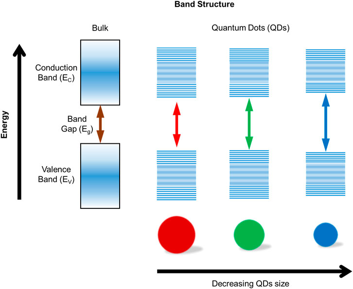
FIGURE 1. Electronic structures of inorganic semiconductors of bulk material, QDs of different diameters.
CQDs, which are synthesized by wet-chemical procedures, refer to semiconductor nanocrystals with typical diameters ranging from 2 to 20 nm (Kagan et al., 2016). Murray et al. (1993) reported the fabrication of CQDs by injecting organometallic reagents into a hot coordinating solvent, which was a breakthrough in the chemical synthesis of QDs. Compared to self-assembled QDs, CQDs benefit from high uniformity in size and low cost provided by colloidal synthesis. In addition, due to the solution-processable character, CQD films can be fabricated by many readily available manufacturing approaches including spin coating, doctor blading, spraying coating, and inkjet printing (Kramer et al., 2015; Garcia de Arquer et al., 2017; Xu et al., 2020). Due to these advantages, CQDs have been appealing materials for solution-processable electronics and optoelectronics, in particular, the PD applications. To date, the most frequently used environmentally friendly CQDs in PDs include nanocrystals of graphene, carbon, and silicon (Si). In addition to PDs based on pure nanocrystals, it has been demonstrated that strategies of doping and functionalization in CQDs can further improve properties of CQDs, resulting in enhanced device performance. Moreover, CQDs combined with other materials to form a heterojunction have demonstrated outstanding PD performance attributed to enhanced light absorption by CQDs and a built-in potential to promote electron–hole pair separation. Finally, due to high compatibility of CQDs, they can be coupled with auxiliary structures, such as plasmonic nanostructures or fabricated on flexible substrates, which satisfies the growing demand in the advanced optoelectronic market.
Working Mechanism and Figures of Merit
Classification of PDs
PDs can be categorized into photoconductors, photodiodes, and phototransistors (Figure 2) (Huo and Konstantatos, 2018; Li et al., 2019; Xu et al., 2020).
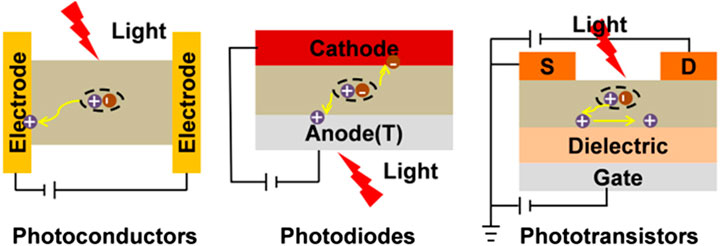
FIGURE 2. Schematic illustrations of typical photoconductors, photodiodes, and phototransistors. T, S, and D stand for transparent, source, and drain, respectively. Reprinted with permission from Chem. Mater., 2019, 31, 6359-6379. Copyright 2019 American Chemical Society.
Photoconductors
A conventional photoconductor has planar structures with two electrodes and a photoactive channel between the two electrodes (Xu et al., 2020). In the photoconductor, photogenerated charge carriers are separated by the applied external bias and then collected at each electrode. In this device configuration, one type of charge carriers is usually localized within the trap states or sensitizing centers with a prolonged lifetime. Meanwhile, the other type of carriers can recirculate through an external circuit until it recombines with its opposite carrier, leading to a photoconductive gain. This gain mechanism results in extremely high external quantum efficiency (EQE) and responsivity compared to a photodiode.
Photodiodes
In a photodiode, photogenerated electrons and holes are separated by the built-in potential formed via a p–n junction or a Schottky junction and then transferred to the opposite electrodes. In some cases, a large external bias is applied to trigger avalanche or carrier multiplication effects, leading to the generation of multiple carriers excited by a single photon and enhanced quantum efficiency. The response speed of the device relies on the transit time of charge carriers defined as:
Phototransistors
To minimize the noise in the photoresponse, a special type of photoconductors, namely, phototransistors, were invented. Compared to conventional photoconductors, phototransistors have an additional gate terminal which is isolated from a channel material by a thin dielectric layer. A gate voltage is applied to modulate the conductivity of the channel and suppress the dark current. In this device structure, the device exhibits high sensitivity because large photoconductive gain and low noise can be achieved at the same time.
Figures of Merit
Photoresponsivity
Photoresponsivity (R) is the ratio of photocurrent (IPh) to the optical power (Pin), defined as Eq. 1 in the unit of AW−1.
External Quantum Efficiency
The EQE represents the ratio of the number of photogenerated carriers (NC) to the number of incident photons (NI) and can be expressed as Eq. 2, where e is the electron charge, λ is the wavelength of illumination, h is the Planck constant, and c is the velocity of light.
Upon incident light, a PD only absorbs a portion of photons depending on the light absorption efficiency (ηA) and the number of absorbed photons can be defined as
Response Time
Response time includes the rise time (τr) and the fall time (τf) which are defined as the time interval for the rise and decay of the photocurrent from 10 to 90% and from 90 to 10%, respectively.
Photoconductive Gain
Photoconductive gain (G) describes the capability to generate multiple charge carriers by a single incident photon. While one type of carrier (e.g., hole) is trapped with a lifetime of τlife, the other type of carrier (e.g., electron) drifts in the external circuit with a transit time of τtransit. If τlife is longer than τtransit, electrons can circulate many times in the channel and result in the photoconductive gain, which is given as Eq. 4, where L, μ, and VDS stand for channel length, carrier mobility, and the bias voltage, respectively.
Noise Equivalent Power
Noise equivalent power (NEP) represents the minimum detectable optical power of a PD where the signal-to-noise ratio (SNR) is 1 (or 0 dB). It is given as Eq. 5 in the unit of W Hz−1/2, where iN is the noise current.
Detectivity
Detectivity (D*), which is used to evaluate the sensitivity of a PD, is a very important figure of merit. It is given as Eq. 6, where A is the active area of the device and B is the electrical bandwidth. The unit of D* is Jones or cm Hz1/2 W−1 and the detectivity enables the comparisons of PDs with different geometries and areas (Long et al., 2018).
Heavy Metal–Free Quantum Dots for Photodetector Applications
Carbon and Graphene Quantum Dots
Graphene QDs (GQDs) and carbon QDs have attracted immense interest as promising candidates for PD application because of their nontoxicity, biocompatibility, and excellent electrical, optical, and physicochemical properties, such as tunable bandgap, high absorptivity, nontoxicity, high stability, and cost-effectiveness (Sun et al., 2006; Pan et al., 2010; Zhang et al., 2015; Tajik et al., 2020; Ghosh et al., 2021). Generally, GQDs have layered structures and possess strong quantum confinement effect with sizes down to 100 nm. On the contrary, carbon QDs have a spherical shape with a diameter up to 10 nm. In addition, GQDs are a derivation of graphene/graphite and other graphitic materials, whereas carbon QDs are generally produced by the bottom-up processes (Pan et al., 2010). Both carbon QDs and GQDs have large bandgap with ability to tune bandgap, and therefore, PDs based on carbon QDs and GQDs are generally applied to detect light near UV (Hai et al., 2018; Jia et al., 2020; Wang et al., 2020).
Conventional Graphene Quantum Dots and Carbon Quantum Dots
Zhang et al. (2015) demonstrated a DUV PD, detecting short wavelength of 254 nm, based on solution-processed GQDs with the large bandgap. As shown in Figure 3A, the authors employed an asymmetric electrode structure (Au and Ag) in PD to improve the sensitivity of the device. The energy band diagram (Figures 3B–D) illustrates the mechanism of charge carrier transport in each device configuration: i) symmetrical Au electrodes structure; ii) symmetrical Ag electrodes structure; and iii) asymmetrical Au and Ag electrodes structure. As illustrated in Figures 3B–D, a barrier for carrier transportation inevitably existed in devices with symmetrical electrodes. On the contrary, the asymmetrical electrodes formed favorable energy band alignment with GQDs, which enabled both photogenerated electrons and holes to drift freely toward the electrodes. This led to the reduced recombination and efficient transport of electrons and holes to the electrodes. As a result, the author demonstrated the superior PD performance with asymmetrical electrodes compared to symmetrical electrodes.
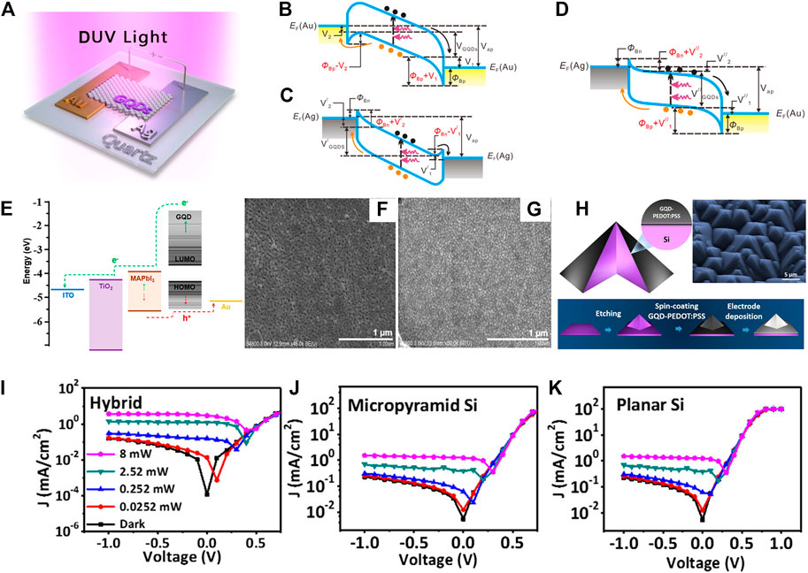
FIGURE 3. (A) Schematic of GQD-based PDs with asymmetric electrodes. (B–D) Schematic diagram of energy band of GQD-based PD with (B) Au/Au, (C) Ag/Ag, and (D) Ag/Au electrodes, respectively. (E) Schematic of energy diagram and carrier transportation mechanism of the GQD/MAPbI3 PD. SEM images of (F) MAPbI3 film and (G) GQD/MAPbI3 film. (H) The structure, SEM image, and the fabrication procedure of the device. I-V curves of (I) the hybrid, (J) micropyramid Si, and (K) planar Si PDs in the dark and under 532 nm incident light with different power. (A–D) Reprinted with permission from ACS Nano, 2015, 9, 1561-1570. Copyright 2015 American Chemical Society. (E–G) Reprinted with permission from ACS Appl. Electron. Mater., 2020, 2, 230-237. Copyright 2020 American Chemical Society. (H–K) Reprinted with permission from ACS Nano, 2017, 11, 4564-4570. Copyright 2017 American Chemical Society.
PDs with a hybrid structure have been introduced to enhance device performances in UV detection as well. Ghosh et al. (2016) employed a hybrid structure of zinc oxide (ZnO) and GQDs or carbon QDs. In the hybrid ZnO–GQD and ZnO–carbon QD devices, electron–hole pairs are generated in both GQDs/carbon QDs and ZnO nanorods, which led to an increase in the responsivity compared to pristine ZnO nanorods. The device displayed the highest photoresponsivity and detectivity of 6.92 × 10⁴ AW−1 and 1.78 × 10¹⁵ Jones, respectively, under 365 nm light and low bias of 2 V. Following this work, recently, Subramanian et al. (2020) have reported a high-performance PD based on the hybrid structure of GQD and high-quality MAPbI3 hybrid film. The addition of GQDs facilitated the light absorption of the device, increasing the generation of charge carriers, and promoted charge transport by forming the junction between GQDs and the MAPbI3 film, as shown in Figure 3E. The LUMO level of the GQDs is higher than that of the MAPbI3 film, and thus, the electron injection from the GQDs to the MAPbI3 film is promoted. Similarly, the HOMO level of the MAPbI3 film is lower than that of the GQDs, leading to an increase in the hole transfer from the MAPbI3 film to the GQDs. In addition, the work demonstrated that high-quality perovskite film could be formed through the passivation of the perovskite film by the GQDs. As a result, fewer number of pinholes were present in the film and consequently reduced trap densities (Figures 3F, G), resulting in efficient charge carrier transport. Under the bias voltage of −3 V, the GQD/MAPbI3 PD achieved a maximum detectivity of 6.5 × 10¹¹ Jones, and the responsivity reached 12 A W-1, which is three times higher than that of the pristine MAPbI3 device. Despite the fact that the strategy of applying GQDs proves to be effective in improving the device performance, employment of MAPbI3 containing the toxic Pb substance would not be ideal for the future environmental-friendly optoelectronics. Further works need to be done to replace Pb2+ with other nontoxic metal cations, such as Cu2+ and Sn2+.
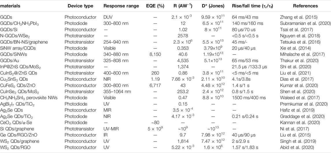
In order to perform effective light detection in the natural environment where the conditions are less optimal, it is essential to develop PDs with high sensitivity and the ability to harvest omnidirectional light. However, traditional PDs often require a cooling system to reduce high noise when detecting weak light, limiting the PD design due to increased cost and complexity (Tsai et al., 2017). To resolve these issues, another type of the hybrid PD was introduced by Tsai et al. (2017) with the GQD-PEDOT:PSS/Si structure. In this hybrid PD, GQD was responsible for enhancing the light absorption in the short wavelength region and increasing the conductivity of the device. The pyramidal structure in microscale was fabricated on Si surface as shown in Figure 3H to harvest omnidirectional photons. The device exhibited an enhancement of responsivity up to 0.9 AW-1 at large angles of incidence (AOIs), ± 75°, compared with the micropyramid Si PD, demonstrating its excellent ability of omnidirectional photodetection. The dark current of the hybrid device was much smaller compared to devices on micropyramid and planar Si (Figures 3I–K). This indicates a low noise level in low-light conditions, which was attributed to a PEDOT:PSS layer that prevented electrons from reaching the top electrode. The parameters of PDs in Figure 3 are collected in Table 1.
Doped/Functionalized GQDs and Carbon QDs
Nitrogen (N) doping of GQDs and carbon QDs enhances the optical and electrical properties of QDs in many aspects, such as improvement in photoluminescence quantum yield (PLQY), higher absorption in visible wavelength, and efficient charge transfer (Nguyen et al., 2018). Because of the improved material properties, N-doped GQDs (N-GQDs) and carbon QDs have demonstrated enhanced PD performance.
A hybrid PD based on a monolayer (ML) tungsten diselenide (WSe2)/N-GQD heterostructure was investigated by Nguyen et al. (2018), as shown in Figure 4A. The author reported 480% of enhanced photoresponsivity compared to that of the pristine ML WSe2 PD (Figure 4B). This significant improvement was ascribed to the strong light absorption of N-GQDs, charge transfer from the N-GQDs to ML WSe2, and the photogating effect by photogenerated electrons in the N-GQD layer as can be seen in the energy band diagram in Figure 4C. Due to the heterojunction formed between N-GQDs and ML WSe2, the photogenerated holes in N-GQDs transferred to ML WSe2. On the contrary, the flow of electrons from N-GQDs to ML WSe2 was prevented, leading to the accumulation of electrons and consequently the photogating effect. The highest photoresponsivity of 2578 AW-1 at VG = −60 V and a power density of 1.9 μWcm−2 were observed. In addition, the author demonstrated a stable photoresponsivity in ambient air with 46% performance retention after 30 days (Figure 4B). In 2019, Wu et al. (2019) constructed all-carbon–based UV PDs by integrating N-doped carbon QDs and graphene. In this device configuration, the carbon QDs and the graphene were employed as the light-absorbing material and the channel of the device, respectively, effectively solving the problem caused by the weak light absorption of graphene. The author reported a maximal responsivity of 2.5 × 10⁴ AW−1.
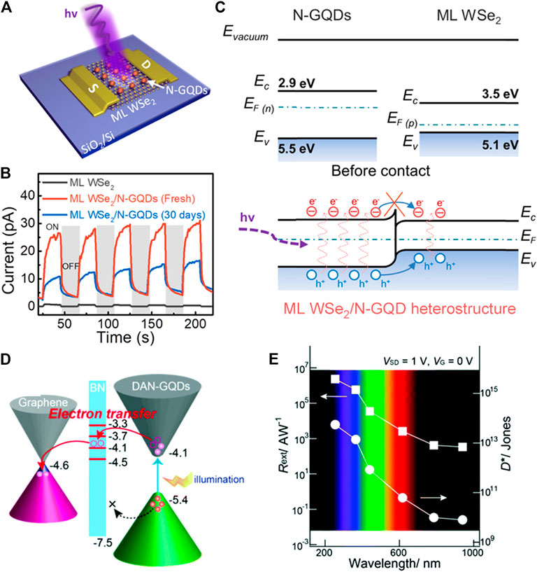
FIGURE 4. (A) Schematic of the hybrid ML WSe2/N-GQD PD. (B) Photocurrent of ML WSe2, ML WSe2/N-GQD devices and after 30 days under ambient condition. (C) Energy band diagram before and after the formation of ML WSe2/N-GQD heterostructure. (D) Schematic illustration of the energy level of the graphene/BN-NS/DAN-GQD hybrid PD under light illumination. (E) Photoresponsivity and detectivity vs. incident power (wavelength ranging from 254 to 940 nm) for the device. (A–C) Reprinted with permission from ACS Appl. Mater. Interfaces, 2018, 10, 10322–10329. Copyright 2018 American Chemical Society. (D–E) Reprinted with permission from Nanoscale, 2016, 8, 19677-19683. Copyright 2016 Royal Society of Chemistry.
Similar to the doping strategy, functionalization of GQDs was also demonstrated by Tetsuka et al. (2016). The author functionalized GQDs with diaminonaphthalene (DAN-GQD) and reported a hybrid PD with the structure of the graphene/BN-NS/DAN-GQD, where boron nitride nanosheets (BN-NSs) were employed as a buffer layer. The BN-NS layer was applied to enhance the separation and transportation of photogenerated carriers through the vacancy states formed in its bandgap from DAN-GQD layer to graphene. As illustrated in Figure 4D, vacancy states formed in the BN-NS layer are located between LUMO levels of graphene and DAN-GQD, allowing only photogenerated electrons to transport from DAN-GQDs to the graphene layer. In contrast, holes remained in the DAN-GQD layer, resulting in the suppression of charge carrier recombination. The device showed high responsivity and detectivity ranging from the DUV to the near-IR region, as shown in Figure 4E. The highest values reached 2.3 × 10⁶ AW−1 and 5.5 × 10¹³ Jones in the DUV region. The parameters of PDs in Figure 4 are collected in Table 1.
Core–Shell Structure
A structure of radial core–shell heterojunction has been developed for PD applications to further enhance charge carrier collections by minimizing the travel distances of the charge carrier smaller or close to the minority carrier diffusion length (Mihalache et al., 2017).
Xie et al. (2014) demonstrated a core–shell heterojunction consisting of Si nanowires (SiNWs) array at the core and carbon QDs at the outer shell for a visible light PD (Figure 5A). Due to the strong light absorption capability of the SiNWs compared to planar Si, more photogenerated carriers were produced by the PD. The excitons were effectively dissociated and transferred to the electrodes because the heterojunction formed between SiNW arrays and carbon QDs induced the built-in potential which effectively blocked backflow of electrons and minimized carrier recombination by confining electrons in SiNWs. As a result, the author achieved a high-performance self-driven PD with large responsivity (353 mAW−1) and fast response speed (rise/fall time = 20/40 μs).
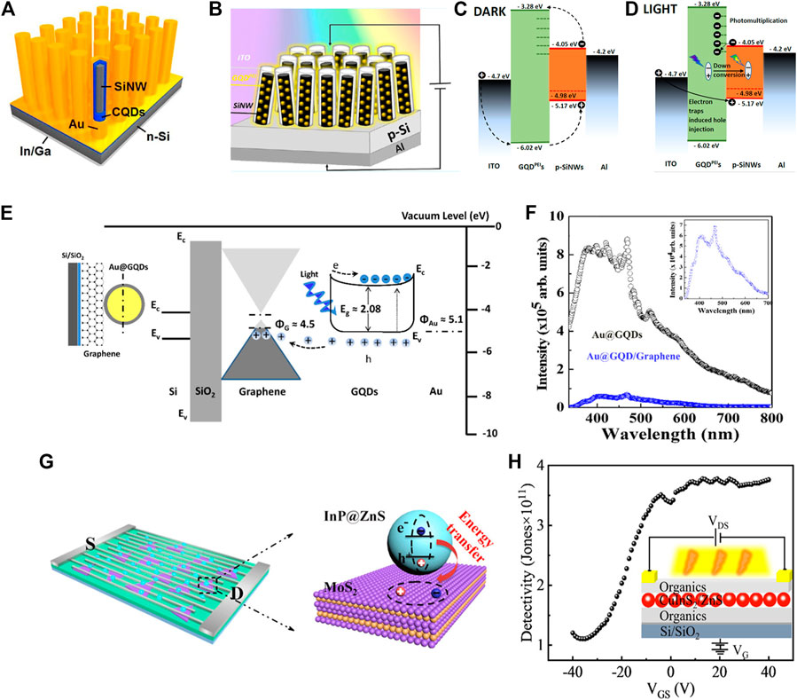
FIGURE 5. (A) The structure of the SiNW array/carbon QD heterojunction device. (B) The schematic of the GQDPEI/SiNW core–shell structure device. Energy band diagram of the ITO/GQDPEI/SiNW/Al device under reverse bias (C) in dark and (D) under illumination. (E) Illustration and energy level diagram of the PD using Au@GQD nanohybrids. (F) PL spectra of Au@GQD (black line) and Au@GQD/graphene (blue line) under incident light of 325 nm with a magnified PL spectrum of Au@GQD/graphene in the inset. (G) Structural diagram and schematic of the InP@ZnS-MoS2 hybrid energy transfer system. (H) Schematic view of the QD photodetector and representative detectivity performance. (A) Reprinted with permission from ACS Nano 2014, 8, 4015–4022. Copyright 2014 American Chemical Society. (B–D) Reprinted with permission from ACS Appl. Mater. Interfaces, 2017, 9, 29234–29247. Copyright 2017 American Chemical Society. (E–F) Reprinted with permission from ACS Appl. Mater. Interfaces, 2020, 12, 28550–28560. Copyright 2020 American Chemical Society. (G) Reprinted with permission from ACS Appl. Mater. Interfaces, 2020, 12, 31382–31391. Copyright 2020 American Chemical Society. (H) Reprinted with permission from ACS Appl. Electron. Mater., 2021, 3, 1236–1243. Copyright 2021 American Chemical Society.
Similarly, Mihalache et al. (2017) reported a core–shell ITO/GQDPEI/SiNW/Al structure PD in which a continuous GQDPEI/ITO film acts as a bilayered shell to envelop the SiNW core (Figure 5B). As illustrated in Figure 5C, the energy band of Si is located between the LUMO and HOMO levels of the GQDPEI, and therefore, a large barrier was created at the interface in the core–shell structure PD. In a dark condition, this reduced the charge transfer to the electrodes, resulting in the suppression of the dark current. Under illumination (Figure 5D), the photogenerated electrons transported to the ITO electrode, while holes swept to the aluminum (Al) back contact. This is because electrons trapped in GQDPEI lowered the hole injection barrier, which facilitated the hole transport. In addition, the author claimed prolonged lifetime of electron and reduced carrier recombination in the employed core–shell structure. Additionally, GQDs exhibited the photon down-conversion effect, absorbing light in the UV and visible region while emitting light at 580 nm. Due to the superior performance of photocurrent conversion of SiNW, the device exhibited extraordinary performance, exhibiting a large photocurrent-to-dark current ratio (Iph/Idark up to ∼ 0.9×10² under 4 V bias) and 8150% of the EQE value at 10 V reverse bias, which was particularly a remarkable improvement compared to other types of heterostructures containing heavy metals, for example, CdTe/SiNW.
Another type of the core–shell structure was introduced by Thakur et al. (2020) with the hybrid structure of Au nanoparticles at the core and GQDs at the outer shell (Au@GQD) using microplasmas. Upon the illumination of light, the Au@GQD core–shell structure absorbed light and photogenerated holes were transported to the graphene layer and ultimately collected at the electrodes, leading to an increase in the photocurrent compared to the structure of with only Au@GQDs (Figure 5E). The author demonstrated this phenomenon through the photoluminescence (PL) quenching of the Au@GQD/graphene device, as shown in Figure 5F. Compared with PDs made of graphene, graphene decorated with Au nanoparticles, and graphene decorated with GQDs, the Au@GQD/graphene device showed photocurrent about four times higher than other control groups, suggesting the merits of the core–shell structure in PD applications.
In addition to the core–shell device structure, environmentally friendly core–shell QDs have been developed and employed for PD applications. Shi et al. (2020) proposed a hybrid PD comprising InP/ZnS core–shell QDs and bilayer MoS2, as shown in Figure 5G. Due to the strong overlap in the absorption spectrum between core–shell QDs and MoS2, plasmon-enhanced nonradiative energy transfer occurred in the hybrid 0D/2D system. The built-in electric field at the asymmetric Pt/MoS2 Schottky junction further enhanced the charge separation and transfer. In addition, the authors applied interdigitated electrodes with Pt-patterned arrays, which enhanced the light harvesting by anti-reflection. As a result, the fabricated phototransistor exhibited excellent performance with responsivity of 1374 AW-1 and ultrafast rise time of 25 μs. Liu et al. (2021) developed highly sensitive PD based on CuInS2/ZnS core–shell QDs (Figure 5H). The authors embedded CuInS2 QDs within ZnS and improved the optical instability of pure CuInS2 QDs by surface passivation. The QD film was sandwiched between two PCBM: Poly-TPD blend organic layers. Under illumination, photogenerated carriers were separated and transported to respective electrodes efficiently due to the favorable energy band alignment at the organic/QD interface, promoting the photocurrent to a large extent. The obtained PD showed a high detectivity of 3.76 × 10¹¹ Jones and EQE of 262%, and a fast rise and fall time <5 ms.
Cu-Based Quantum Dots
Copper (Cu) is one of the earth-abundant materials and mostly exists in the forms of compounds in nature. In recent years, a variety of Cu-based QDs have been employed for heavy metal–free CQD-based PDs.
One example of Cu-based CQDs is copper tin sulfide (Cu2SnS3), which is a p-type semiconductor, consisting of inexpensive and nontoxic elements, with a high absorption coefficient greater than 104 cm−1. Dias et al. (2017) utilized Cu2SnS3 CQDs for NIR photodetection, as shown in Figure 6A. Poly(vinylpyrrolidone) (PVP) was used as a surfactant to effectively prevent the agglomeration of CQDs. Another example of Cu-based CQDs was reported by Liu et al. (2019). The author employed copper oxide (Cu2O) CQDs to develop a graphene/Cu2O QD/Cu PD based on an internal photocurrent gain mechanism. Driven by the built-in electric field, photogenerated electrons in Cu2O CQDs transferred to the Cu electrode, while holes migrated toward the graphene layer. Accordingly, the Fermi level of graphene decreased from equilibrium, and consequently, carriers were injected from electrodes to the graphene layer. This led to the increase in the carrier density, resulting in an amplified photocurrent. The device exhibited high responsivity of 1.2 × 10¹⁰ AW−1 and the capacity of detecting femtowatt-scale light at room temperature. In addition, after applying excessive bending, the device still showed decent photoresponse, demonstrating its promising potential for flexible PDs.
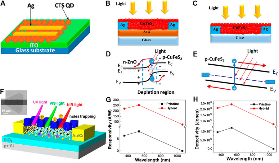
FIGURE 6. (A) Schematic diagram of the PD based on Cu2SnS3 QDs. Schematic illustration of (B) the CuFeS2 QD/ZnO heterojunction PD and (C) the single-layer CuFeS2 QD PD. Schematic diagrams of energy band and charge transfer of (D) the heterojunction PD and (E) the single-layer PD. (F) Schematics of the hybrid FET. (G) Photoresponsivity and (H) specific detectivity of the device as a function of wavelength. (A) Reprinted with permission from Inorg. Chem., 2017, 56, 2198–2203. Copyright 2017 American Chemical Society. (B–E) Reprinted with permission from ACS Omega, 2020, 5, 25947–25953. Copyright 2020 American Chemical Society. (F–H) Reprinted with permission from ACS Appl. Mater. Interfaces, 2020, 12, 54927–54935. Copyright 2020 American Chemical Society.
Copper iron sulfide (CuFeS2) CQD is another preferable semiconductor for PDs owing to its abundancy and tunable bandgap from ∼ 0.55 to 1.0 eV by controlling its particle size. Kumar et al. (2020) fabricated a PD based on a bilayer heterojunction of CuFeS2 QDs and ZnO layers. Compared to PDs of single-layer CuFeS2 QDs, the effective separation of electron–hole pairs driven by the electric field at the heterojunction considerably reduced carrier recombination (Figures 6B–E). As a result, the detectivity of the device reached above 1012 Jones in visible and NIR regions at a bias of 10 V. Similarly, Sugathan et al. (2020) fabricated a hybrid PD based on CuFeS2 QDs and Si with an extended photodetection spectrum from 460 to 2,200 nm. In addition, the device exhibited fall time of 20 μs in the NIR region, which is faster than that of PDs based on bulk Si (typically few milliseconds to seconds).
Copper indium selenide (CuInSe2) QDs possess a stable phase structure, high extinction coefficient, and narrow bandgap and have demonstrated great potential for photodetection. Shen et al. (2020) hybridized CuInSe2 QDs with ML molybdenum disulfide (MoS2) and fabricated the first MoS2-based PD with broadband photoresponse up to 1,064 nm (Figure 6F). Benefiting from the photogating effect and the favorable type-II energy band alignment between CuInSe2 QDs and MoS2, the device showed enhanced responsivity and detectivity which is about 30 and 20 times higher than that of the pristine MoS2 PD, respectively, as shown in Figures 6G,H. Additionally, the depletion region formed at the CuInSe2 QDs and MoS2 interface enabled the slow minority carriers (i.e., holes) to escape from the localized states, improving rise time from 58 to 0.8 s. In addition, Guo et al. (2021) doped transition metal manganese ions (Mn2+) into CuInSe2 QDs to improve the low responsivity of the QDs caused by poor crystal quality and high trap density and verified the effectiveness of this strategy in a PD. The optimized device exhibited remarkable improvement of photoresponse compared to PDs based on pristine CuInSe2 QDs, such as high detectivity of 4.2 × 10¹² Jones and fast response of 0.76 μs. Such performance is comparable to some Pb-based CQD PDs, demonstrating the great potential of CuInSe2 QDs as environmentally friendly alternatives for NIR photodetection. The parameters of PDs in Figure 6 are collected in Table 1.
Perovskite Quantum Dots
We now turn our attention to the newly emerging perovskite CQDs (PQDs). PQDs have attracted tremendous attention worldwide as a promising photoactive material due to their excellent electrical and optoelectrical properties, such as long lifetime and diffusion length, superiorities in luminescent, tunable bandgap, and the facile processing technique (Jellicoe et al., 2016; Kajari-Schröder, 2019). Because of this, optoelectronic devices based on various dimensional perovskite materials, namely, 3D, 2D, and 0D PQDs, have demonstrated outstanding device performance comparable to their counterparts. For example, Dou et al. (2014) demonstrated the solution-processed hybrid perovskite PDs using an inverted device configuration with high device performances for the first time. However, PQDs and other perovskite materials contain heavy metals, Pb and/or Cd, which are highly toxic to the environment and human causing cancer (Babayigit et al., 2016; Kajari-Schröder, 2019). Therefore, there have been efforts to synthesize Pb-free PQDs in recent years, as shown in Figures 7A,B (Wang et al., 2016; Tong et al., 2017; Yang et al., 2017; Zhang et al., 2017; Ji et al., 2018; Zhou et al., 2018; Ke and Kanatzidis, 2019; Yang et al., 2019; Ma et al., 2020). Compared to other optoelectronic devices based on perovskite materials, however, heavy metal–free PQDs and their PD applications have attracted less attention so far. This might be due to the difficulties in the synthesis of Pb-free PQDs as well as low device performance compared to Pb-free 2D/3D perovskite films, resulting from the low crystallinity, prominent charge-carrier trapping, and short charge-carrier lifetimes of these PQDs (Bai et al., 2021). In spite of this fact, it is still of importance to develop nontoxic and nonhazardous PQD-based PDs as they offer facile bandgap tunability and consequently good selectivity of response range. So far, some achievements have been made in PDs based on Pb-free PQDs as well as other dimensional perovskite materials. It is worth noting that as nanostructured Pb-free perovskite-based PDs are still under intensive development in recent years, noncolloidal methods are also included to broaden a readership and our perspectives.
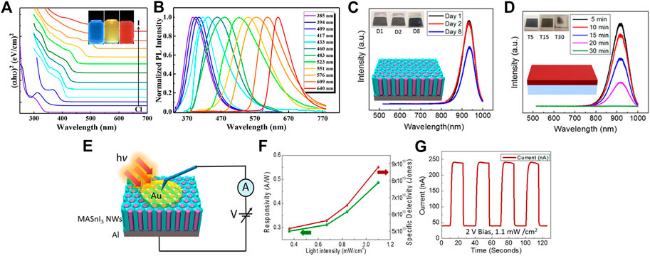
FIGURE 7. (A) PL and (B) absorption characteristics of Cs3Sb2X9 QDs where the inset shows PQDs under UV light excitation. Photographs of as-obtained colloidal Cs3Bi2X9 (X = Cl, Cl0.5Br0.5, Br, Br0.5I0.5, I). (C) PL characteristics of Sn perovskite NWs where inset shows the Sn perovskite NWs after 1, 2, and 8 days. (D) PL characteristics of Sn perovskite thin films where inset shows Sn perovskite thin film sample after 5, 15, and 30 min. (E) Schematics of the Sn-based perovskite NW PD. (F) Responsivity and specific detectivity of the PD. (G) I–t curve of the PD at the light intensity of 1.1 mW/cm2 (2 V bias voltage). (A–B) Reprinted with permission from ACS Energy Lett., 2020, 5, 385–394. Copyright 2020 American Chemical Society. (C–G). Reprinted with permission from Nano Lett., 2017, 17, 523–530. Copyright 2017 American Chemical Society.
Ghosh et al. (2018) synthesized cesium–tin–iodine (Cs2SnI6)–based PQDs with different morphologies (nanocubes, nanorods, and small and large 2D nanosheets) and fabricated PDs based on each morphology. The author reported high photocurrent gain in PDs, demonstrating 15, 20, and 475 for nanocubes, nanosheets, and nanorods, respectively. In particular, the PD with the nanorods exhibited the best photoresponse time, achieving 1 s of both rise and fall time of the photocurrent, whereas the PD with the nanosheet showed the highest responsivity and detectivity values, approximately, 130 AW-1 and 1013 Jones, respectively. Similarly, Ghosh et al. (2020) reported all-inorganic bismuth (Bi) (III)–based PQDs to achieve better stability and lower toxicity, which are attributed to the absence of Pb compound and the absence of the volatile nature of the methylammonium cation (Leng et al., 2016; Lou et al., 2018; Nelson et al., 2018; Tran et al., 2020). Using the stable PQDs in an ambient condition, the author demonstrated the photocurrent gain (IPhoto/IDark) up to 53 at the applied bias 5 V from Cs3Br2I9 PQDs under the light illumination (solar simulator, 0.65 W/cm−2). Recently, Bai et al. (2021) have reported, for the first time, quadruple colloidal PQDs, such as Cs4MnSb2Cl12 and Cs4MnBi2Cl12, for highly sensitive PDs to overcome high instability of Sn-based PQDs. The author reported 96-fold and 77-fold increase in PLQY and PL lifetime in Cs4MnBi2Cl12 PQDs, and the PD based on this PQD demonstrated high responsivity, detectivity, and EQE up to 860 AW-1, 4.5 × 10¹⁰ Jones, and 2.9 × 10⁵%, respectively, under 365 nm wavelength light source.
In addition to colloidal PQDs, Waleed et al. (2017) synthesized 1D perovskite nanowires (NWs) using a chemical vapor method to enhance the stability. The vulnerability of the Sn-based perovskites to moistures and oxygen is due to the fast lateral diffusion of the water and oxygen molecules along the grain boundaries in perovskite films (Frost et al., 2014; Manser et al., 2016). 1D-structured Sn-based perovskites effectively prevented the lateral diffusion of the oxygen and water molecules, demonstrating high material and device stability compared to the Sn-based perovskite film, as shown in Figures 7C,D. The PD (Figure 7E) exhibited responsivity up to 0.47 AW-1 with the specific detectivity of 8.80 × 10¹⁰ Jones and photocurrent rise and fall time of 1500 and 400 ms, respectively, under the periodically switched halogen light, as shown in Figures 7F,G. The parameters of PDs in Figure 7 are collected in Table 1.
These results demonstrated promising future of the heavy metal–free nanostructured perovskites and their PD applications. However, the device performance still lags behind that of the other counterparts, such as PDs based on PbS QDs and Pb-based perovskite films. So as to achieve green electronics and optoelectronics, intensive investigation on heavy metal–free PQDs is needed.
Other Types of Quantum Dots
Xing et al. (2018) reported a photoelectrochemical (PEC)-type PD based on Bi QDs. Due to the strong interactions between Bi QDs and light, a significant number of electron–hole pairs were generated, and consequently, the device produced a strong photocurrent without any external bias, showing its excellent self-driven performance. In addition, even after immersing the device in alkaline electrolytes for 1 month without any protection, the PD still remained 50% of the original photocurrent, which demonstrated its long-term stability in liquid. Following this work, Premkumar et al. (2020) constructed PDs based on three types of silver bismuth iodide QDs including AgBiI4, Ag2BiI5, and AgBi2I7 (Figure 8A). Oleylamine and oleic acid were used as ligands for controlling the crystal size and minimizing the defect states. Due to the long excited-state lifetime in QDs and the suitable energy band alignment between QDs and TiO2, photogenerated electrons transferred to TiO2 with minimum energy losses. The PD based on AgBi2I7 exhibited the best photoresponse performance among the fabricated three types, with responsivity of 0.15 AW-1 at the wavelength of 390 nm.
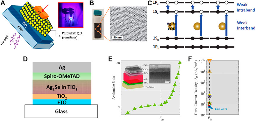
FIGURE 8. (A) Schematics of AgBi2I7 QDs–based UV PD and photographic image of device testing under UV light. (B) A digital image of Ag2Se CQD solution and a corresponding TEM image. (C) Schematic illustration of carrier distribution in Ag2Se QDs. The intraband gap is the bandgap for MIR absorption. Blue lines represent possible optical transitions. (D) Schematic structure of the PD based on Ag2Se QDs in a mesoporous TiO2 scaffold. (E) Avalanche gain and (F) dark current density of the CeO2 QD–based PD. (A). Reprinted with permission from ACS Appl. Nano Mater., 2020, 3, 9141–9150. Copyright 2020 American Chemical Society. (B–C) Reprinted with permission from ACS Appl. Nano Mater., 2019, 2, 1631-1636. Copyright 2019 American Chemical Society. (D) Reprinted with permission from ACS Appl. Nano Mater., 2020, 3, 12209-12217. Copyright 2020 American Chemical Society. (E–F) Reprinted with permission from ACS Photon., 2020, 7, 1367-1374. Copyright 2020 American Chemical Society.
MIR photodetection based on CQDs has reached a high level of maturity with various Hg chalcogenides compounds, denoted as HgX where X indicates chalcogenides compounds, for example, HgS, HgSe, and HgTe. Due to the metal-rich surface feature, excess electrons are located at the conduction band in the HgX compounds. The optical transitions of electrons within the conduction band result in strong absorption in MIR spectrum. Similarly, Ag2Se CQDs, which possess very similar metal-rich surface chemistry to HgX compounds, have demonstrated MIR absorption and therefore been considered as a green alternative for MIR PDs (Martinez et al., 2017; Qu et al., 2018). Qu et al. (2018) integrated Ag2Se QDs into an electrolyte-gated transistor. However, the device exhibited very limited photoresponse performance and bias stability below 200 mV, which might be caused by the reduction of Ag+. Similarly, Hafiz et al. (2019) fabricated a PD based on Ag2Se QDs (Figure 8B) and investigated the effect of ligand exchange on photoresponse performance. The fabricated Ag2Se QDs had excess electrons which were located at the first conduction energy level (1Se). The authors reported that the optical transition from 1Se to the second conduction energy level (1Pe) led to the stronger MIR absorbance (Figure 8C). According to measured absorbance and spectral photoresponse, the ligand exchange of QDs with 1,2-ethanedithiol (EDT) reduced the concentration of excess electrons and had a detrimental influence on their capacity as light absorbers. To improve the responsivity, the authors suggested increasing the doping concentration in QDs for providing more electrons in the 1Se state, which led to a stronger MIR absorbance. In addition to MIR photodetection, Ag2Se QDs demonstrated NIR light harvesting. Similarly, Graddage et al. (2020) reported the first Ag2Se QD–based photodiode (Figure 8D) with high sensitivity ranging from 1,000 to 1,400 nm. To improve the precursor reactivity, the authors applied secondary phosphine and realized accurate QD size control. To fabricate a PD, QDs were deposited into a mesoporous TiO2 scaffold to enhance optical absorption and charge carrier separation. In particular, 2,2′,7,7′-Tetrakis[N,N-di(4-methoxyphenyl)amino]-9,9′-spirobifluorene (Spiro-OMeTAD) was used as a hole transport layer because its HOMO energy level (−5.0 eV) matches well with the valence band of Ag2Se QDs (−4.86 eV), which ensured efficient carrier collection. The device exhibited responsivity of 4.17 mAW−1 and a high on and off ratio of 490 at the wavelength of 1,200 nm.
Furthermore, metallic oxide–based CQDs have been employed in PDs as a hole blocking layer (HBL) or light absorber as well (Kannan et al., 2020; Lin et al., 2020). Kannan et al. (2020) deposited CeO2 QD film on an amorphous selenium (α-Se) film as the HBL for avalanche photodiodes (APDs). Due to the large bandgap of CeO2 QDs, ∼ 3.77 eV, the CeO2 QD layer effectively blocked holes. As a result, the author achieved an avalanche gain of 42 using 40 nm CeO2 HBL and the lowest dark current density of JD ∼ 30 pA/cm2 ever reported (Figures 8E,F). In 2020, another type of metallic oxide QDs, Ga2O3 CQDs, was introduced to overcome the low photoresponse of all-Si–based PDs in the DUV region. Lin et al. (2020) developed a vertically stacked graphene/Ga2O3 QD/Si photodiode, where Ga2O3 QDs were used as a DUV sensitive layer. Upon illumination, the separation of photogenerated electron–hole pairs was promoted by the Ga2O3 QD/Si heterojunction. In addition, graphene layer significantly enhanced the absorption area of the PD for harvesting more photons. As a result, the device showed high photoresponsivity under DUV illumination and the highest EQE reached 80.2% without external bias, which is twice that of all-Si PDs. The parameters of PDs in Figure 8 are collected in Table 1.
The 0D/2D structure using various environmentally friendly QDs has been widely adopted to further improve PD performances as well. For example, Si is a principal material used in commercial PDs due to its abundance, nontoxicity, and stability. However, the application of Si PDs is largely limited by the small and indirect bandgap and weak light absorption over the visible-NIR range, resulting in low photoresponse of Si-based PDs. As an alternative to overcome the drawbacks of bulk Si, the combination of Si QDs (SQDs) and 2D materials have been demonstrated as an effective strategy for a future Si-based high-performance PD. The hybrid 0D/2D structure greatly improves light absorption capacity and dissociation of photogenerated charge carriers, which is attributed to the QD layer and the formation of the heterojunction, respectively (Konstantatos et al., 2012; Hu et al., 2016; Ra et al., 2016; Huo et al., 2017; Pak et al., 2018; Qiao et al., 2020). Shin et al. (2015) fabricated the first PD based on a SQD-embedded SiO2 (SQD:SiO2) and graphene heterojunction. The bandgap energy of SQDs within the SiO2 matrix was measured to be varied in the range of 1.4–1.8 eV, enabling photodetection of a higher energy range compared to bulk Si. The fabricated heterostructure 0D/2D PD showed high detectivity of approximately 109 cm Hz1/2W−1, which is about ten times higher than that of bulk-Si/graphene Schottky diodes (An et al., 2013). In addition, Yu et al. (2016) demonstrated a SQD/graphene heterojunction on a Si substrate. The Fermi level of graphene was lowered after coupled with SQDs because of electron transfer from graphene to SQDs, resulting in a larger built-in potential and a wider depletion region. Therefore, the separation of photogenerated carriers was effectively promoted, leading to the improved photoresponse. Following this work, Ni et al. (2017) demonstrated a broadband phototransistor based on a heterostructure of boron (B)-doped SQDs and graphene (Figure 9A). According to ultraviolet photoelectron spectroscopy (UPS) study, the work function of SQDs and graphene are -4.62 and -4.78 eV, respectively, indicating the electron transfer from SQDs to graphene (Figure 9B). After the Fermi level of SQDs and graphene reached equilibrium, upward bending of energy bands occurred at the interface, resulting in the transportation of photogenerated holes from SQDs to graphene, as shown in Figure 9C. Two optical phenomena related to SQDs can be exploited upon illumination. In the MIR region, the localized surface plasmon resonance (LSPR) of B-doped Si QDs induced an electric field, which enhanced light absorption of the underlying graphene. The optical absorption of SQDs from the UV to NIR region led to a photogating effect, resulting in improved photoconductive gain. As a result, the fabricated PD showed maximum responsivity of 2.2 × 10⁹ and 44.9 AW-1, and the highest detectivity on the orders of 1013 and 105 Jones under UV–NIR and MIR illumination, respectively, as shown in Figures 9D,E. Hu et al. (2019) fabricated a heterostructure utilizing InGaN QD and 2D graphene sheet. The resulting hybrid PD featured ultrahigh responsivity and detectivity of 1.6 × 10⁹ AW−1 and 5.8 × 10¹⁴ Jones, respectively. The authors demonstrated its high sensitivity of detecting light on the femtowatt level at room temperature without extra signal processing.
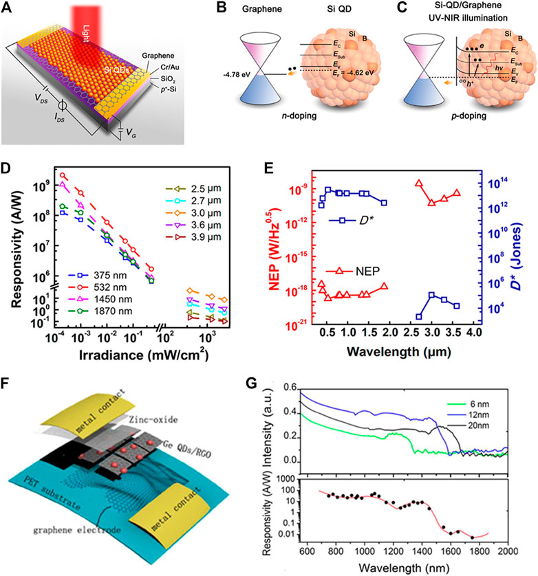
FIGURE 9. (A) Schematics of the hybrid PD. Energy band diagram of graphene and Si QDs and schematics of charge transfer in the heterostructure (B) in dark and (C) under UV-to-NIR illumination. (D) Responsivity of the device as a function of irradiance intensity. (E) NEP and specific detectivity of the device as a function of wavelength. (F) Device schematics of the heterostructure PD. (G) Responsivity of the device as a function of wavelength. (A–E) Reprinted with permission from ACS Nano, 2017, 11, 9854–9862. Copyright 2017 American Chemical Society. (F–G). Reprinted with permission from ACS Appl. Mater. Interfaces, 2015, 7, 2452–2458. Copyright 2015 American Chemical Society.
As another nontoxic semiconductor of group IV, germanium (Ge) shares many similar characteristics with Si. In addition, Ge has a narrower bandgap (0.67 eV), which enables photodetection to IR range. Liu et al. (2015) fabricated an IR PD by decorating Ge QDs onto reduced graphene oxide (RGO), and the QD-decorated RGO/ZnO heterostructure is shown in Figure 9F. The authors achieved the most effective energy transfer between QDs and RGO by tailoring the diameter of Ge QDs. In addition, the Schottky barrier formed between ZnO and RGO contributed to the high on and off ratio (∼103) of the IR Ge-based PD. Dark current was reduced due to the formation of the energy barrier which restricted the backflow of carriers. Furthermore, when the PD was exposed to incident light, the energy barrier virtually disappeared, which facilitated the charge transfer from RGO to ZnO under reverse bias. As a result, large photocurrent was generated in the device. The hybrid PD exhibited high responsivity (9.7 AW-1) and detectivity (7.98×10¹² Jones) under IR illumination of 1,400 nm, as shown in Figure 9G. The parameters of PDs in Figure 9 are collected in Table 1.
Finally, we turn our attention to another type of the heterojunction employing new types of QDs which are based on 2D TMDCs. 2D TMDCs have drawn increasing research interest in the field of photodetection because of their excellent electrical and optical properties (Jiang et al., 2017). To further control lateral quantum confinement of 2D nanostructures, in recent years, TMDC QDs have been synthesized and introduced to optoelectronic applications (Gopalakrishnan et al., 2015; Jin et al., 2016; Jin et al., 2017). For example, Singh et al. (2019) reported a UV PD based on WS2 QD/graphene heterojunction in 2019. The fabricated PD had high sensitivity in UV photodetection, which was attributed to the strong absorption of WS2 QDs in the UV region. Upon UV illumination, a large number of electron–hole pairs were generated in QDs. As illustrated in Figure 10A, the photogenerated electrons moved toward the graphene layer while holes remained in WS2 QDs. These electrons were transported to an electrode with a high speed due to excellent electron mobility of graphene, resulting in a large photocurrent and fast response time. In this device configuration, the WS2 QDs acted as an effective light-harvesting material, whereas the graphene layer provided a pathway for high-speed carrier transportation. Under incident light of 365 nm, the PD showed high responsivity and detectivity of 1,814 AW-1 and 7.47 × 10¹² Jones, respectively, as shown in Figure 10B. Following this work, Abid et al. (2020) developed a heterojunction of reduced graphene oxide (RGQ) and WS2 QDs on e-textile fabric (Figure 10C). Compared to graphene, easily processable RGO offered simplified synthesis procedures and consequently device fabrication. The device showed no significant changes after bending, twisting, and stretching experiments, demonstrating its robust performance as a flexible PD. The parameters of PDs in Figure 10 are collected in Table 1.
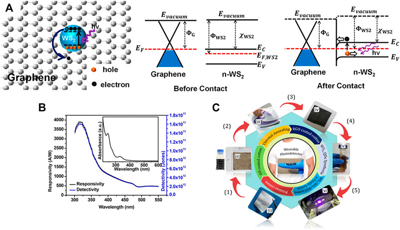
FIGURE 10. (A) Schematic of dispersed WS2 QD on the graphene layer. The energy band diagrams of WS2 QDs/graphene heterojunction before and after contact. (B) Responsivity and detectivity of the PD with an absorption spectrum of WS2 QDs in the inset. (C) Schematic illustration of procedures involved in synthesizing WS2-QDs decorated RGO e-textile–based PD. Images of (ⅰ) pristine cotton textile, (ⅱ) cotton textile coated with GO, (ⅲ) iron used for thermally reducing GO, (ⅳ) GO (or RGO) after thermal reduction, (ⅴ) synthesized solution of WS2 QDs, and (ⅵ) fabricated PD based on WS2 QDs/RGQ heterostructure. (a)–(b) Reprinted with permission from ACS Appl. Nano Mater., 2019, 2, 3934–3942. Copyright 2019 American Chemical Society. (c) Reprinted with permission from ACS Appl. Mater. Interfaces 2020, 12, 39730–39744. Copyright 2020 American Chemical Society.
Discussion
To date, the performance of PDs based on heavy metal–free CQDs has been significantly enhanced through material engineering and device structure optimization. However, most devices are still at early stages of development and there is still a long way to go before transitioning them out of lab and into the market. Further improvements are to be expected to solve remaining challenges and boost their future commercialization.
An open challenge is the implementation of CQD-based PDs with good photoresponse in the MIR region for night vision, aerospace, and astronomy imaging applications. Currently, the majority of CQD-based PDs have limited photodetection spectrum below 2 μm, which is less competitive compared to HgSe and HgTe QDs that can cover the light spectrum up to 20 μm (Lhuillier et al., 2013; Keuleyan et al., 2014; Lhuillier et al., 2016). In this regard, Ag2Se QDs having a small bandgap and an absorption wavelength up to 6.5 μm are an attractive material for the targeted applications (Sahu et al., 2012). A precise doping of QDs has been suggested to have electrons filled up in the 1Se state to prompt intraband absorption between the 1Se and 1Pe state (Hafiz et al., 2019). This novel strategy will open up great opportunities of IR PDs that go beyond traditional interband absorption.
In addition, the long-term stability of CQD PDs to withstand humidity, temperature variation, and photodegradation is an important issue for their practical applications to ensure the great performance in ambient air. Some QDs, such as Si nanocrystals, have intrinsic characteristics of stability, and therefore, they are suitable for long-life applications. Furthermore, strategies to increase the device lifetime have been proposed. For example, passivation of devices with a thin aluminum oxide (Al2O3) film is one of the widespread approaches, which has demonstrated effective passivation of PDs based on PbS and PbSe CQDs to increase their air stability (Ihly et al., 2011; Otto et al., 2013; Hu et al., 2016; Litvin et al., 2017). Additionally, it was reported that the deposited Al2O3 film led to additional electron transport channels, and consequently increased photocurrent (So et al., 2015). Han et al. (2020) incorporated ZnO nanocrystalline film in lateral PDs and efficiently improved response speed and stability based on gradient trapping effect. Similar strategies can be applied to improve the stability of PDs based on heavy metal–free CQDs.
Finally, economic aspect of CQD production and device fabrication for large-scale commercialization is worth consideration. To minimize the production cost of the materials and devices, it is desirable to develop cost-efficient and facile scalable techniques with access to inexpensive processing facilities and low energy synthetic methods (Park et al., 2004; Nightingale et al., 2013; Tian et al., 2016; Yang et al., 2018). In addition, as for device fabrication, a particular issue of the severe performance loss when fabricating PDs in ambient air needs to be resolved.
Conclusion
This review introduced the recent advances of state-of-the-art PDs based on toxic and hazardous heavy metal–free CQDs. First, fundamentals of CQDs and PDs were discussed to provide a comprehensive understanding of QD-based PD applications. Then, we summarized the development of PDs employing different heavy metal–free CQDs in various development aspects. Heavy metal–free CQDs have been compelling candidates for photodetection due to their promising optical and electronic properties as well as eco-friendliness. Tremendous progress has been made during the past decade through material engineering and device geometry tailoring. Despite the significant progresses, intensive work is still required for making laboratory ideas mature into practical applications. We believe that this review article provides a comprehensive summary of heavy metal–free CQD and PD applications and offers insights into building future green optoelectronics and sustainable society.
Author Contributions
SM performed the literature review and wrote the manuscript under the supervision of YC.
Funding
This work was financially supported by the National Natural Science Foundation of China, grant number 52050410331.
Conflict of Interest
The authors declare that the research was conducted in the absence of any commercial or financial relationships that could be construed as a potential conflict of interest.
Acknowledgments
YC would like to acknowledge the University of Michigan–Shanghai Jiao Tong University Joint Institution for supporting this work.
References
Abid, P., Sehrawat, C. M., and Islam, S. S. (2020). WS2 Quantum Dots on E-Textile as a Wearable UV Photodetector: How Well Reduced Graphene Oxide Can Serve as a Carrier Transport Medium? ACS Appl. Mater. Inter. 12, 39730–39744. doi:10.1021/acsami.0c08028
An, X., Liu, F., Jung, Y. J., and Kar, S. (2013). Tunable Graphene-Silicon Heterojunctions for Ultrasensitive Photodetection. Nano Lett. 13 (3), 909–916. doi:10.1021/nl303682j
Babayigit, A., Ethirajan, A., Muller, M., and Conings, B. (2016). Toxicity of Organometal Halide Perovskite Solar Cells. Nat. Mater 15, 247–251. doi:10.1038/nmat4572
Bai, T., Yang, B., Chen, J., Zheng, D., Tang, Z., Wang, X., et al. (2021). Efficient Luminescent Halide Quadruple‐Perovskite Nanocrystals via Trap‐Engineering for Highly Sensitive Photodetectors. Adv. Mater. 33, 2007215. doi:10.1002/adma.202007215
Cho, Y., Giraud, P., Hou, B., Lee, Y.-W., Hong, J., Lee, S., et al. (2017). Charge Transport Modulation of a Flexible Quantum Dot Solar Cell Using a Piezoelectric Effect. Adv. Energ. Mater. 8 (3), 1700809. doi:10.1002/aenm.201700809
Cho, Y., Hou, B., Lim, J., Lee, S., Pak, S., Hong, J., et al. (2018a). Balancing Charge Carrier Transport in a Quantum Dot P-N Junction toward Hysteresis-free High-Performance Solar Cells. ACS Energ. Lett. 3 (4), 1036–1043. doi:10.1021/acsenergylett.8b00130
Cho, Y., Lee, S., Hong, J., Pak, S., Hou, B., Lee, Y.-W., et al. (2018b). Sustainable Hybrid Energy Harvester Based on Air Stable Quantum Dot Solar Cells and Triboelectric Nanogenerator. J. Mater. Chem. A. 6 (26), 12440–12446. doi:10.1039/C8TA03870H
Dias, S., Kumawat, K., Biswas, S., and Krupanidhi, S. B. (2017). Solvothermal Synthesis of Cu2SnS3 Quantum Dots and Their Application in Near-Infrared Photodetectors. Inorg. Chem. 56, 2198–2203. doi:10.1021/acs.inorgchem.6b02832
Dou, L., Yang, Y., You, J., Hong, Z., Chang, W.-H., Li, G., et al. (2014). Solution-processed Hybrid Perovskite Photodetectors with High Detectivity. Nat. Commun. 5, 5404. doi:10.1038/ncomms6404
Frost, J. M., Butler, K. T., Brivio, F., Hendon, C. H., van Schilfgaarde, M., and Walsh, A. (2014). Atomistic Origins of High-Performance in Hybrid Halide Perovskite Solar Cells. Nano Lett. 14 (5), 2584–2590. doi:10.1021/nl500390f
García de Arquer, F. P., Armin, A., Meredith, P., and Sargent, E. H. (2017). Solution-processed Semiconductors for Next-Generation Photodetectors. Nat. Rev. Mater. 2 (3), 16100. doi:10.1038/natrevmats.2016.100
Ghosh, D., Kapri, S., and Bhattacharyya, S. (2016). Phenomenal Ultraviolet Photoresponsivity and Detectivity of Graphene Dots Immobilized on Zinc Oxide Nanorods. ACS Appl. Mater. Inter. 8, 35496–35504. doi:10.1021/acsami.6b13037
Ghosh, D., Sarkar, K., Devi, P., Kim, K.-H., and Kumar, P. (2021). Current and Future Perspectives of Carbon and Graphene Quantum Dots: From Synthesis to Strategy for Building Optoelectronic and Energy Devices. Renew. Sustain. Energ. Rev. 135, 110391. doi:10.1016/j.rser.2020.110391
Ghosh, S., Mukhopadhyay, S., Paul, S., Pradhan, B., and De, S. K. (2020). Control Synthesis and Alloying of Ambient Stable Pb-free Cs3Bi2Br9(1-x)I9x (0 ≤ X ≤ 1) Perovskite Nanocrystals for Photodetector Application. ACS Appl. Nano Mater. 3 (11), 11107–11117. doi:10.1021/acsanm.0c02288
Ghosh, S., Paul, S., and De, S. K. (2018). Control Synthesis of Air-Stable Morphology Tunable Pb-free Cs2 SnI6 Perovskite Nanoparticles and Their Photodetection Properties. Part. Part. Syst. Charact. 35, 1800199. doi:10.1002/ppsc.201800199
Gopalakrishnan, D., Damien, D., Li, B., Gullappalli, H., Pillai, V. K., Ajayan, P. M., et al. (2015). Electrochemical Synthesis of Luminescent MoS2 Quantum Dots. Chem. Commun. 51, 6293–6296. doi:10.1039/C4CC09826A
Graddage, N., Ouyang, J., Lu, J., Chu, T.-Y., Zhang, Y., Li, Z., et al. (2020). Near-Infrared-II Photodetectors Based on Silver Selenide Quantum Dots on Mesoporous TiO2 Scaffolds. ACS Appl. Nano Mater. 3, 12209–12217. doi:10.1021/acsanm.0c02686
Guo, R., Meng, J., Lin, W., Liu, A., Pullerits, T., Zheng, K., et al. (2021). Manganese Doped Eco-Friendly CuInSe2 Colloidal Quantum Dots for Boosting Near-Infrared Photodetection Performance. Chem. Eng. J. 403, 126452. doi:10.1016/j.cej.2020.126452
Guyot-Sionnest, P. (2008). Colloidal Quantum Dots. Comptes Rendus Physique 9 (8), 777–787. doi:10.1016/j.crhy.2008.10.006
Hafiz, S. B., Scimeca, M. R., Zhao, P., Paredes, I. J., Sahu, A., and Ko, D.-K. (2019). Silver Selenide Colloidal Quantum Dots for Mid-wavelength Infrared Photodetection. ACS Appl. Nano Mater. 2, 1631–1636. doi:10.1021/acsanm.9b00069
Hai, X., Feng, J., Chen, X., and Wang, J. (2018). Tuning the Optical Properties of Graphene Quantum Dots for Biosensing and Bioimaging. J. Mater. Chem. B 6, 3219–3234. doi:10.1039/C8TB00428E
Han, T., Xu, Y., Shou, M., Xie, Z., Ying, L., Jiang, C., et al. (2020). Energy Level Gradient Trapping Based on Different Work Functions of ZnO Enhancing Response and Stablity for Lateral Photodetectors. Org. Elect. 86, 105883. doi:10.1016/j.orgel.2020.105883
Hao, Q., Tang, X., Cheng, Y., and Hu, Y. (2020). Development of Flexible and Curved Infrared Detectors with HgTe Colloidal Quantum Dots. Infrared Phys. Tech. 108, 103344. doi:10.1016/j.infrared.2020.103344
Hou, B., Kim, B. S., Lee, H. K. H., Cho, Y., Giraud, P., Liu, M., et al. (2020). Multiphoton Absorption Stimulated Metal Chalcogenide Quantum Dot Solar Cells under Ambient and Concentrated Irradiance. Adv. Funct. Mater. 30, 2004563. doi:10.1002/adfm.202004563
Hu, A., Tian, H., Liu, Q., Wang, L., Wang, L., He, X., et al. (2019). Graphene on Self-Assembled InGaN Quantum Dots Enabling Ultrahighly Sensitive Photodetectors. Adv. Opt. Mater. 7, 1801792. doi:10.1002/adom.201801792
Hu, C., Dong, D., Yang, X., Qiao, K., Yang, D., Deng, H., et al. (2016). Synergistic Effect of Hybrid PbS Quantum Dots/2D-WSe2Toward High Performance and Broadband Phototransistors. Adv. Funct. Mater. 27, 1603605. doi:10.1002/adfm.201603605
Huo, N., Gupta, S., and Konstantatos, G. (2017). MoS2 -HgTe Quantum Dot Hybrid Photodetectors beyond 2 Μm. Adv. Mater. 29, 1606576. doi:10.1002/adma.201606576
Huo, N., and Konstantatos, G. (2018). Recent Progress and Future Prospects of 2D-Based Photodetectors. Adv. Mater. 30, 1801164. doi:10.1002/adma.201801164
Ihly, R., Tolentino, J., Liu, Y., Gibbs, M., and Law, M. (2011). The Photothermal Stability of PbS Quantum Dot Solids. ACS Nano 5 (10), 8175–8186. doi:10.1021/nn2033117
Jellicoe, T. C., Richter, J. M., Glass, H. F. J., Tabachnyk, M., Brady, R., Dutton, S. E., et al. (2016). Synthesis and Optical Properties of lead-free Cesium Tin Halide Perovskite Nanocrystals. J. Am. Chem. Soc. 138 (9), 2941–2944. doi:10.1021/jacs.5b13470
Ji, C., Wang, P., Wu, Z., Sun, Z., Li, L., Zhang, J., et al. (2018). Inch-size Single crystal of a lead-free Organic-Inorganic Hybrid Perovskite for High-Performance Photodetector. Adv. Funct. Mater. 28, 1705467. doi:10.1002/adfm.201705467
Jia, J., Sun, Y., Zhang, Y., Liu, Q., Cao, J., Huang, G., et al. (2020). Facile and Efficient Fabrication of Bandgap Tunable Carbon Quantum Dots Derived from Anthracite and Their Photoluminescence Properties. Front. Chem. 8, 123. doi:10.3389/fchem.2020.00123
Jiang, L., Zeng, S., Ouyang, Q., Dinh, X.-Q., Coquet, P., Qu, J., et al. (2017). Graphene-TMDC-graphene Hybrid Plasmonic Metasurface for Enhanced Biosensing: A Theoretical Analysis. Phys. Status Solidi A. 214, 1700563. doi:10.1002/pssa.201700563
Jin, H., Ahn, M., Jeong, S., Han, J. H., Yoo, D., Son, D. H., et al. (2016). Colloidal Single-Layer Quantum Dots with Lateral Confinement Effects on 2D Exciton. J. Am. Chem. Soc. 138 (40), 13253–13259. doi:10.1021/jacs.6b06972
Jin, H., Baek, B., Kim, D., Wu, F., Batteas, J. D., Cheon, J., et al. (2017). Effects of Direct Solvent-Quantum Dot Interaction on the Optical Properties of Colloidal Monolayer WS2 Quantum Dots. Nano Lett. 17 (12), 7471–7477. doi:10.1021/acs.nanolett.7b03381
Kagan, C. R., Lifshitz, E., Sargent, E. H., and Talapin, D. V. (2016). Building Devices from Colloidal Quantum Dots. Science 353 (6302)), aac5523. doi:10.1126/science.aac5523
Kannan, H., Stavro, J., Mukherjee, A., Léveillé, S., Kisslinger, K., Guan, L., et al. (2020). Ultralow Dark Currents in Avalanche Amorphous Selenium Photodetectors Using Solution-Processed Quantum Dot Blocking Layer. ACS Photon. 7, 1367–1374. doi:10.1021/acsphotonics.9b01651
Ke, W., and Kanatzidis, M. G. (2019). Prospects for Low-Toxicity lead-free Perovskite Solar Cells. Nat. Commun. 10, 965. doi:10.1038/s41467-019-08918-3
Keuleyan, S. E., Guyot-Sionnest, P., Delerue, C., and Allan, G. (2014). Mercury Telluride Colloidal Quantum Dots: Electronic Structure, Size-dependent Spectra, and Photocurrent Detection up to 12 μm. ACS Nano 8 (8), 8676–8682. doi:10.1021/nn503805h
Konstantatos, G., Badioli, M., Gaudreau, L., Osmond, J., Bernechea, M., de Arquer, F. P. G., et al. (2012). Hybrid Graphene-Quantum Dot Phototransistors with Ultrahigh Gain. Nat. Nanotech 7, 363–368. doi:10.1038/nnano.2012.60
Kramer, I. J., Minor, J. C., Moreno-Bautista, G., Rollny, L., Kanjanaboos, P., Kopilovic, D., et al. (2015). Efficient spray-coated Colloidal Quantum Dot Solar Cells. Adv. Mater. 27 (1), 116–121. doi:10.1002/adma.201403281
Kumar, B., Singh, S. V., Chattopadhyay, A., Biring, S., and Pal, B. N. (2020). Scalable Synthesis of a Sub-10 Nm Chalcopyrite (CuFeS2) Nanocrystal by the Microwave-Assisted Synthesis Technique and its Application in a Heavy-metal-free Broad-Band Photodetector. ACS Omega 5, 25947–25953. doi:10.1021/acsomega.0c03336
Leng, M., Chen, Z., Yang, Y., Li, Z., Zeng, K., Li, K., et al. (2016). Lead-free, Blue Emitting Bismuth Halide Perovskite Quantum Dots. Angew. Chem. Int. Ed. 55, 15012–15016. doi:10.1002/ange.20160816010.1002/anie.201608160
Lhuillier, E., Keuleyan, S., Liu, H., and Guyot-Sionnest, P. (2013). Mid-IR Colloidal Nanocrystals. Chem. Mater. 25 (8), 1272–1282. doi:10.1021/cm303801s
Lhuillier, E., Scarafagio, M., Hease, P., Nadal, B., Aubin, H., Xu, X. Z., et al. (2016). Infrared Photodetection Based on Colloidal Quantum-Dot Films with High Mobility and Optical Absorption up to THz. Nano Lett. 16 (2), 1282–1286. doi:10.1021/acs.nanolett.5b04616
Li, J., Xia, J., Liu, Y., Zhang, S., Teng, C., Zhang, X., et al. (2019). Ultrasensitive Organic‐Modulated CsPbBr 3 Quantum Dot Photodetectors via Fast Interfacial Charge Transfer. Adv. Mater. Inter. 7, 1901741. doi:10.1002/admi.201901741
Li, Q., Guo, Y., and Liu, Y. (2019). Exploration of Near-Infrared Organic Photodetectors. Chem. Mater. 31 (17), 6359–6379. doi:10.1021/acs.chemmater.9b00966
Lin, R., Kan, H., Zheng, W., and Huang, F. (2020). Ligand Tailoring Oxide Colloidal Quantum Dots for Silicon‐Integrated Ultraviolet Photodiode. Adv. Electron. Mater. 6, 1901238. doi:10.1002/aelm.201901238
Litvin, A. P., Martynenko, I. V., Purcell-Milton, F., Baranov, A. V., Fedorov, A. V., and Gun'ko, Y. K. (2017). Colloidal Quantum Dots for Optoelectronics. J. Mater. Chem. A. 5, 13252–13275. doi:10.1039/c7ta02076g
Liu, Q., Tian, H., Li, J., Hu, A., He, X., Sui, M., et al. (2019). Hybrid Graphene/Cu 2 O Quantum Dot Photodetectors with Ultrahigh Responsivity. Adv. Opt. Mater. 7, 1900455. doi:10.1002/adom.201900455
Liu, X., Ji, X., Liu, M., Liu, N., Tao, Z., Dai, Q., et al. (2015). High-performance Ge Quantum Dot Decorated Graphene/zinc-Oxide Heterostructure Infrared Photodetector. ACS Appl. Mater. Inter. 7 (4), 2452–2458. doi:10.1021/am5072173
Liu, Y., Zhao, C., Li, J., Zhao, S., Xu, X., Fu, H. Y., et al. (2021). Highly Sensitive CuInS2/ZnS Core-Shell Quantum Dot Photodetectors. ACS Appl. Electron. Mater. 3 (3), 1236–1243. doi:10.1021/acsaelm.0c01064
Long, M., Wang, P., Fang, H., and Hu, W. (2018). Progress, Challenges, and Opportunities for 2D Material Based Photodetectors. Adv. Funct. Mater. 29, 1803807. doi:10.1002/adfm.201803807
Lou, Y., Fang, M., Chen, J., and Zhao, Y. (2018). Formation of Highly Luminescent Cesium Bismuth Halide Perovskite Quantum Dots Tuned by Anion Exchange. Chem. Commun. 54, 3779–3782. doi:10.1039/C8CC01110A
Ma, Z., Shi, Z., Yang, D., Zhang, F., Li, S., Wang, L., et al. (2020). Electrically-Driven Violet Light-Emitting Devices Based on Highly Stable Lead-Free Perovskite Cs3Sb2Br9 Quantum Dots. ACS Energ. Lett. 5 (2), 385–394. doi:10.1021/acsenergylett.9b02096
Manser, J. S., Saidaminov, M. I., Christians, J. A., Bakr, O. M., and Kamat, P. V. (2016). Making and Breaking of lead Halide Perovskites. Acc. Chem. Res. 49, 330–338. doi:10.1021/acs.accounts.5b00455
Martinez, B., Livache, C., Notemgnou Mouafo, L. D., Goubet, N., Keuleyan, S., Cruguel, H., et al. (2017). HgSe Self-Doped Nanocrystals as a Platform to Investigate the Effects of Vanishing Confinement. ACS Appl. Mater. Inter. 9, 36173–36180. doi:10.1021/acsami.7b10665
Mihalache, I., Radoi, A., Pascu, R., Romanitan, C., Vasile, E., and Kusko, M. (2017). Engineering Graphene Quantum Dots for Enhanced Ultraviolet and Visible Light P-Si Nanowire-Based Photodetector. ACS Appl. Mater. Inter. 9, 29234–29247. doi:10.1021/acsami.7b07667
Murray, C. B., Norris, D. J., and Bawendi, M. G. (1993). Synthesis and Characterization of Nearly Monodisperse CdE (E = Sulfur, Selenium, Tellurium) Semiconductor Nanocrystallites. J. Am. Chem. Soc. 115 (19), 8706–8715. doi:10.1021/ja00072a025
Nelson, R. D., Santra, K., Wang, Y., Hadi, A., Petrich, J. W., and Panthani, M. G. (2018). Synthesis and Optical Properties of Ordered-Vacancy Perovskite Cesium Bismuth Halide Nanocrystals. Chem. Commun. 54, 3640–3643. doi:10.1039/C7CC07223F
Nguyen, D. A., Oh, H. M., Duong, N. T., Bang, S., Yoon, S. J., and Jeong, M. S. (2018). Highly Enhanced Photoresponsivity of a Monolayer WSe2 Photodetector with Nitrogen-Doped Graphene Quantum Dots. ACS Appl. Mater. Inter. 10, 10322–10329. doi:10.1021/acsami.7b18419
Ni, Z., Ma, L., Du, S., Xu, Y., Yuan, M., Fang, H., et al. (2017). Plasmonic Silicon Quantum Dots Enabled High-Sensitivity Ultrabroadband Photodetection of Graphene-Based Hybrid Phototransistors. ACS Nano 11 (10), 9854–9862. doi:10.1021/acsnano.7b03569
Nightingale, A. M., Bannock, J. H., Krishnadasan, S. H., O'Mahony, F. T. F., Haque, S. A., Sloan, J., et al. (2013). Large-scale Synthesis of Nanocrystals in a Multichannel Droplet Reactor. J. Mater. Chem. A. 1 (12), 4067–4076. doi:10.1039/c3ta10458c
Otto, T., Miller, C., Tolentino, J., Liu, Y., Law, M., and Yu, D. (2013). Gate-dependent Carrier Diffusion Length in lead Selenide Quantum Dot Field-Effect Transistors. Nano Lett. 13 (8), 3463–3469. doi:10.1021/nl401698z
Pak, S., Cho, Y., Hong, J., Lee, J., Lee, S., Hou, B., et al. (2018). Consecutive Junction-Induced Efficient Charge Separation Mechanisms for High-Performance MoS2/Quantum Dot Phototransistors. ACS Appl. Mater. Inter. 10, 38264–38271. doi:10.1021/acsami.8b14408
Pan, D., Zhang, J., Li, Z., and Wu, M. (2010). Hydrothermal Route for Cutting Graphene Sheets into Blue-Luminescent Graphene Quantum Dots. Adv. Mater. 22 (6), 734–738. doi:10.1002/adma.200902825
Park, J., An, K., Hwang, Y., Park, J.-G., Noh, H.-J., Kim, J.-Y., et al. (2004). Ultra-large-scale Syntheses of Monodisperse Nanocrystals. Nat. Mater 3 (12), 891–895. doi:10.1038/nmat1251
Premkumar, S., Liu, D., Zhang, Y., Nataraj, D., Ramya, S., Jin, Z., et al. (2020). Stable lead-free Silver Bismuth Iodide Perovskite Quantum Dots for UV Photodetection. ACS Appl. Nano Mater. 3, 9141–9150. doi:10.1021/acsanm.0c01787
Qiao, H., Li, Z., Huang, Z., Ren, X., Kang, J., Qiu, M., et al. (2020). Self-powered Photodetectors Based on 0D/2D Mixed Dimensional Heterojunction with Black Phosphorus Quantum Dots as Hole Accepters. Appl. Mater. Today 20, 100765. doi:10.1016/j.apmt.2020.100765
Qu, J., Goubet, N., Livache, C., Martinez, B., Amelot, D., Gréboval, C., et al. (2018). Intraband Mid-infrared Transitions in Ag2Se Nanocrystals: Potential and Limitations for Hg-free Low-Cost Photodetection. J. Phys. Chem. C 122, 18161–18167. doi:10.1021/acs.jpcc.8b05699
Ra, H.-S., Kwak, D.-H., and Lee, J.-S. (2016). A Hybrid MoS2nanosheet-CdSe Nanocrystal Phototransistor with a Fast Photoresponse. Nanoscale 8, 17223–17230. doi:10.1039/C6NR05393A
Sahu, A., Khare, A., Deng, D. D., and Norris, D. J. (2012). Quantum Confinement in Silver Selenide Semiconductor Nanocrystals. Chem. Commun. 48, 5458–5460. doi:10.1039/c2cc30539a
Shen, T., Li, F., Zhang, Z., Xu, L., and Qi, J. (2020). High-Performance Broadband Photodetector Based on Monolayer MoS2 Hybridized with Environment-Friendly CuInSe2 Quantum Dots. ACS Appl. Mater. Inter. 12, 54927–54935. doi:10.1021/acsami.0c14161
Shi, K., Li, J., Xiao, Y., Guo, L., Chu, X., Zhai, Y., et al. (2020). High-Response, Ultrafast-Speed, and Self-Powered Photodetection Achieved in InP@ZnS-MoS2 Phototransistors with Interdigitated Pt Electrodes. ACS Appl. Mater. Inter. 12 (28), 31382–31391. doi:10.1021/acsami.0c05476
Shin, D. H., Kim, S., Kim, J. M., Jang, C. W., Kim, J. H., Lee, K. W., et al. (2015). Graphene/Si-quantum-dot Heterojunction Diodes Showing High Photosensitivity Compatible with Quantum Confinement Effect. Adv. Mater. 27 (16), 2614–2620. doi:10.1002/adma.201500040
Singh, V. K., M. Yadav, S., Mishra, H., Kumar, R., Tiwari, R. S., Pandey, A., et al. (2019). WS2 Quantum Dot Graphene Nanocomposite Film for UV Photodetection. ACS Appl. Nano Mater. 2, 3934–3942. doi:10.1021/acsanm.9b00820
So, H.-M., Choi, H., Shim, H. C., Lee, S.-M., Jeong, S., and Chang, W. S. (2015). Atomic Layer Deposition Effect on the Electrical Properties of Al2O3-Passivated PbS Quantum Dot Field-Effect Transistors. Appl. Phys. Lett. 106 (9), 093507. doi:10.1063/1.4914304
Subramanian, A., Akram, J., Hussain, S., Chen, J., Qasim, K., Zhang, W., et al. (2020). High-Performance Photodetector Based on a Graphene Quantum Dot/CH3NH3PbI3 Perovskite Hybrid. ACS Appl. Electron. Mater. 2, 230–237. doi:10.1021/acsaelm.9b00705
Sugathan, A., Saigal, N., Rajasekar, G. P., and Pandey, A. (2020). Copper Iron Sulfide Nanocrystal‐Bulk Silicon Heterojunctions for Broadband Photodetection. Adv. Mater. Inter. 7, 2000056. doi:10.1002/admi.202000056
Sun, Y.-P., Zhou, B., Lin, Y., Wang, W., Fernando, K. A. S., Pathak, P., et al. (2006). Quantum-sized Carbon Dots for Bright and Colorful Photoluminescence. J. Am. Chem. Soc. 128 (24), 7756–7757. doi:10.1021/ja062677d
Tajik, S., Dourandish, Z., Zhang, K., Beitollahi, H., Le, Q. V., Jang, H. W., et al. (2020). Carbon and Graphene Quantum Dots: a Review on Syntheses, Characterization, Biological and Sensing Applications for Neurotransmitter Determination. RSC Adv. 10 (26), 15406–15429. doi:10.1039/D0RA00799D
Tetsuka, H., Nagoya, A., and Tamura, S.-i. (2016). Graphene/nitrogen-functionalized Graphene Quantum Dot Hybrid Broadband Photodetectors with a Buffer Layer of boron Nitride Nanosheets. Nanoscale 8, 19677–19683. doi:10.1039/C6NR07707B
Thakur, M. K., Fang, C.-Y., Yang, Y.-T., Effendi, T. A., Roy, P. K., Chen, R.-S., et al. (2020). Microplasma-Enabled Graphene Quantum Dot-Wrapped Gold Nanoparticles with Synergistic Enhancement for Broad Band Photodetection. ACS Appl. Mater. Inter. 12, 28550–28560. doi:10.1021/acsami.0c06753
Tian, S., Fu, M., Hoheisel, W., and Mleczko, L. (2016). Reaction Engineering Studies of the Continuous Synthesis of CuInS 2 and CuInS 2 /ZnS Nanocrystals. Chem. Eng. J. 289, 365–373. doi:10.1016/j.cej.2015.12.086
Tong, X.-W., Kong, W.-Y., Wang, Y.-Y., Zhu, J.-M., Luo, L.-B., and Wang, Z.-H. (2017). High-Performance Red-Light Photodetector Based on Lead-Free Bismuth Halide Perovskite Film. ACS Appl. Mater. Inter. 9 (22), 18977–18985. doi:10.1021/acsami.7b04616
Tran, M. N., Cleveland, I. J., and Aydil, E. S. (2020). Resolving the Discrepancies in the Reported Optical Absorption of Low-Dimensional Nontoxic Perovskites, Cs3Bi2Br9 and Cs3BiBr6. J. Mater. Chem. C 8, 10456–10463. doi:10.1039/D0TC02783A
Tsai, M. L., Tsai, D. S., Tang, L., Chen, L.-J., Lau, S. P., and He, J. H. (2017). Omnidirectional Harvesting of Weak Light Using a Graphene Quantum Dot-Modified Organic/silicon Hybrid Device. ACS Nano 11, 4564–4570. doi:10.1021/acsnano.6b08567
Waleed, A., Tavakoli, M. M., Gu, L., Wang, Z., Zhang, D., Manikandan, A., et al. (2017). Lead-free Perovskite Nanowire Array Photodetectors with Drastically Improved Stability in Nanoengineering Templates. Nano Lett. 17 (1), 523–530. doi:10.1021/acs.nanolett.6b04587
Wang, A., Yan, X., Zhang, M., Sun, S., Yang, M., Shen, W., et al. (2016). Controlled Synthesis of Lead-Free and Stable Perovskite Derivative Cs2SnI6 Nanocrystals via a Facile Hot-Injection Process. Chem. Mater. 28 (22), 8132–8140. doi:10.1021/acs.chemmater.6b01329
Wang, L., Li, W., Yin, L., Liu, Y., Guo, H., Lai, J., et al. (2020). Full-color Fluorescent Carbon Quantum Dots. Sci. Adv. 6 (40), eabb6772. doi:10.1126/sciadv.abb6772
Wu, X., Zhao, B., Zhang, J., Xu, H., Xu, K., and Chen, G. (2019). Photoluminescence and Photodetecting Properties of the Hydrothermally Synthesized Nitrogen-Doped Carbon Quantum Dots. J. Phys. Chem. C 123, 25570–25578. doi:10.1021/acs.jpcc.9b06672
Xie, C., Nie, B., Zeng, L., Liang, F.-X., Wang, M.-Z., Luo, L., et al. (2014). Core-shell Heterojunction of Silicon Nanowire Arrays and Carbon Quantum Dots for Photovoltaic Devices and Self-Driven Photodetectors. ACS Nano 8 (4), 4015–4022. doi:10.1021/nn501001j
Xing, C., Huang, W., Xie, Z., Zhao, J., Ma, D., Fan, T., et al. (2018). Ultrasmall Bismuth Quantum Dots: Facile Liquid-phase Exfoliation, Characterization, and Application in High-Performance UV-Vis Photodetector. ACS Photon. 5, 621–629. doi:10.1021/acsphotonics.7b01211
Xu, K., Zhou, W., and Ning, Z. (2020). Integrated Structure and Device Engineering for High Performance and Scalable Quantum Dot Infrared Photodetectors. Small 16, 2003397. doi:10.1002/smll.202003397
Yang, B., Chen, J., Hong, F., Mao, X., Zheng, K., Yang, S., et al. (2017). Lead‐Free, Air‐Stable All‐Inorganic Cesium Bismuth Halide Perovskite Nanocrystals. Angew. Chem. Int. Ed. 56, 12471–12475. doi:10.1002/anie.201704739
Yang, J., Bao, C., Ning, W., Wu, B., Ji, F., Yan, Z., et al. (2019). Stable, High‐Sensitivity and Fast‐Response Photodetectors Based on Lead‐Free Cs 2 AgBiBr 6 Double Perovskite Films. Adv. Opt. Mater. 7, 1801732. doi:10.1002/adom.201801732
Yang, Z., Gao, M., Wu, W., Yang, X., SunZhang, X. W. J., Zhang, J., et al. (2019). Recent Advances in Quantum Dot-Based Light-Emitting Devices: Challenges and Possible Solutions. Mater. Today 24, 69–93. doi:10.1016/j.mattod.2018.09.002
Yu, T., Wang, F., Xu, Y., Ma, L., Pi, X., and Yang, D. (2016). Graphene Coupled with Silicon Quantum Dots for High-Performance Bulk-Silicon-Based Schottky-junction Photodetectors. Adv. Mater. 28 (24), 4912–4919. doi:10.1002/adma.201506140
Zhang, J., Yang, Y., Deng, H., Farooq, U., Yang, X., khan, j., et al. (2017). High Quantum Yield Blue Emission from lead-free Inorganic Antimony Halide Perovskite Colloidal Quantum Dots. ACS Nano 11 (9), 9294–9302. doi:10.1021/acsnano.7b04683
Zhang, Q., Jie, J., Diao, S., Shao, Z., Zhang, Q., Wang, L., et al. (2015). Solution-processed Graphene Quantum Dot Deep-UV Photodetectors. ACS Nano 9 (2), 1561–1570. doi:10.1021/acsnano.5b00437
Zhao, H., and Rosei, F. (2017). Colloidal Quantum Dots for Solar Technologies. Chem 3 (2), 229–258. doi:10.1016/j.chempr.2017.07.007
Keywords: colloidal quantum dots, heavy metals, environmental friendliness, photodetectors, green optoelectronics
Citation: Miao S and Cho Y (2021) Toward Green Optoelectronics: Environmental-Friendly Colloidal Quantum Dots Photodetectors. Front. Energy Res. 9:666534. doi: 10.3389/fenrg.2021.666534
Received: 10 February 2021; Accepted: 20 May 2021;
Published: 16 June 2021.
Edited by:
Mengxia Liu, University of Cambridge, United KingdomReviewed by:
Letian Dou, Purdue University, United StatesXin Tong, University of Electronic Science and Technology of China, China
Copyright © 2021 Miao and Cho. This is an open-access article distributed under the terms of the Creative Commons Attribution License (CC BY). The use, distribution or reproduction in other forums is permitted, provided the original author(s) and the copyright owner(s) are credited and that the original publication in this journal is cited, in accordance with accepted academic practice. No use, distribution or reproduction is permitted which does not comply with these terms.
*Correspondence: Yuljae Cho, eXVsamFlLmNob0BzanR1LmVkdS5jbg==