- 1Electrical and Computer Engineering Department, Advanced Power Electronics Centre (APEC), Khalifa University, Abu Dhabi, United Arab Emirates
- 2Applied Power Electronics Laboratory (APEL), Electrical and Electronics Engineering Department, Indian Institute of Technology Bombay (IITB), Mumbai, India
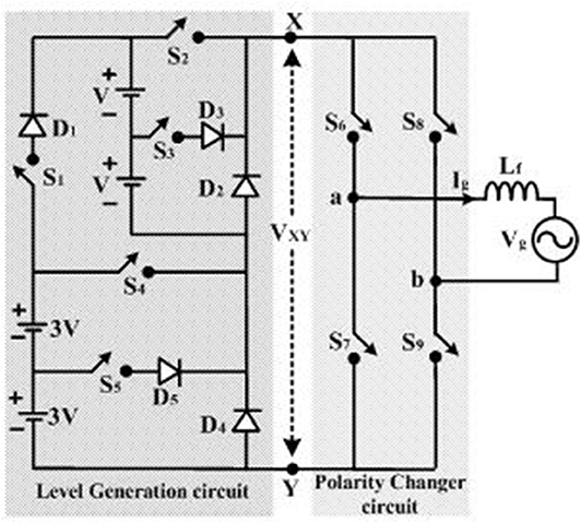
In this paper, a new seventeen level inverter topology is proposed for single-phase grid-connected renewable energy applications. The proposed inverter topology can provide seventeen levels in the output voltage while using a lesser number of power devices. This proposed inverter topology comprises nine power switches, five power diodes, and two sets of DC sources (two 3 V and two V) which are in the ratio of 1:3. By properly arranging the input DC sources, power switches, and power diodes through different possible combinations the seventeen voltage levels are generated. The main advantage of this seventeen level inverter is that a maximum of six power devices conducts in any mode. Thus, conduction losses are lesser compared to existing seventeen level inverter topologies which results in a highly efficient system. Further, the detailed comparison of proposed inverter topology with the existing multilevel inverter (MLI) topologies shows that the number of required power devices count is considerably lower. The possible extension of the proposed inverter topology for the three-phase application is also discussed. Further, a level-shifted based pulse modulation strategy is proposed to control the output of the proposed inverter. To verify the operation, the proposed inverter topology is simulated in MATLAB/Simulink for a 500 W grid-connected system. All the major results are included in the paper. The experiments are performed to validate the proposed inverter topology for a 500 W grid-connected system and all the key results are included in the paper.
Introduction
In the present days, the grid integrated renewable energy systems are drawing huge attention due to their several advantages. Solar photovoltaics (PV) is the most popular renewable energy source among the existing renewable energy sources. However, the grid integration of solar PV involves several challenges. To realize high voltage source from low voltage solar PV modules requires a series connection of several PV modules which may lead to module mismatch and partial shading problems (Sharma and Agarwal, 2014). The alternate solution is to use a low voltage PV module with the high gain DC-DC converter as a frontend to the inverter for boosting the output voltage to be compatible with the 1-ϕ, 230 V or 3-ϕ, 415 V grid. Another alternate solution is to use the line-frequency transformer at the output of the PV inverter. But the use of additional transformer increases system cost, size, and losses in the system. This demands the utilization of high voltage gain DC-DC converters (Liu and Li, 2006; Tao et al., 2006; Duarte et al., 2007; Das and Agarwal, 2016) at the front end for boosting the voltage from low voltage solar PV source. The important features which are required from the high voltage gain DC-DC converters are that they should provide high voltage gain while maintaining high efficiency which is not possible with the conventional switched-mode DC-DC converters. To fulfill the above-mentioned requirements, the special high gain DC-DC converter topologies were proposed and developed. Another interesting feature of these high gain DC-DC converters is that they have isolated multi outputs which is more suitable for multi-input DC-AC inverter for interfacing with utility grid or load.
Figure 1 shows the typical block diagram of the grid-connected renewable energy source [PV or fuel cell (FC)] fed high gain DC-DC converter based multi-input DC-AC converter system. Here, the single input and multioutput DC-DC converter do the maximum power point tracking (MPPT) of the PV/FC source. The isolated multi-outputs of the high gain DC-DC converter acts as multi inputs of the MLI. The multi-inputs of the MLI can be regulated either through the grid side converter control (shown in Figure 1A) or battery supported DC-DC converter (shown in Figure 1B). Additionally, the configurations are shown in Figure 1 will not allow the flow of common-mode current into the grid due to the galvanic isolation between the PV source and the grid. This paper concerns a novel multi-input MLI topology as a solution to this requirement.
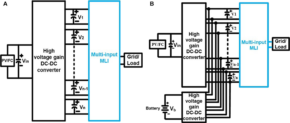
Figure 1. The multi-input DC-AC converter based grid-connected PV/FC systems. (A) DC-DC converter fed Multi input MLI. (B) Battery supported DC-DC converter fed Multi input MLI.
Nowadays multilevel inverters (MLIs) have been gaining huge popularity as a single-stage inverter for renewable energy applications (Rodriguez et al., 2002; Lezana et al., 2008; Peng et al., 2010). The stepped output voltage waveform can be realized in MLIs through various arrangements of power devices using several input DC sources. Due to their salient features, MLIs became very suitable for medium voltage and high power applications compared to two-level converters. The applications of MLIs are not only limited to solar PV systems (Essakiappan et al., 2015) but also for wind energy systems (Yuan, 2014), drive systems (Ahmadi and Wang, 2014), and active power filters (Mathew et al., 2013). Even though MLIs require more number of power devices (Phanikumar and Agarwal, 2013a,b), they are still looked after due to their several advantages. They are lesser THD in output voltage, lesser filter requirement, lesser dv/dt, and lower electromagnetic interference (EMI). The conventional MLIs are classified as diode clamped (Nabae Takahashi and Akagi, 1981), capacitor clamped (Meynard and Foch, 1992), and cascaded H-bridge (Peng et al., 1996) MLIs.
The diode clamped and capacitor clamped MLIs are not preferred by researchers over CHB MLI due to their several drawbacks (Zare, 2008). Because they require large capacitors, unbalance in the voltages of input DC capacitors, and high voltage stress across power devices. Moreover, the CHB MLI accommodates a lesser number of power devices among conventional MLIs to produce the same number of voltage levels in the output (Gupta et al., 2016). The elementary concept of CHB MLI is to produce a staircase output voltage waveform through several combinations of power devices and DC sources. For solar PV applications, these DC sources can be replaced with solar PV modules as well. The presence of several steps in the output voltage waveform produces the higher quality sinusoidal waveform with a small output filter. But with the increase in the number of steps (i.e., the number of levels “n”) in the output voltage, the number of power devices count also increases rapidly.
The researchers in Zare (2008) and Gupta et al. (2016) have done an extensive literature review on the state of the art of various topologies of MLIs. The authors in Babaei and Hosseini (2009) considered two power switches for a DC source to generate one positive voltage level. These modules are cascaded in series, and their output is connected to a full-bridge inverter to generate both positive and negative voltage levels. The authors in Babaei et al. (2014b) have modified the MLI topology in Babaei and Hosseini (2009) by adding two DC capacitors in each module with the DC source to achieve more levels in modules. In this topology, each module requires one full-bridge inverter which increases the number of components in the system.
Another type of MLI topologies which accommodate unequal input DC sources also can produce high quality of output. These topologies are called as asymmetrical MLI topologies. The advantage of these topologies is the requirement of a reduced number of power devices compared to conventional CHB MLI topologies. These topologies use fewer power components with optimal use of input DC sources. The authors in Gupta and Jain (2012) and Farhadi Kangarlu and Babaei (2013) uses a cross-connection of switches to produce more number of levels in the output with reduced stress on the devices. Further, extended MLI topologies with unequal DC sources were proposed in Babaei et al. (2014c) and Babaei et al. (2014a). Even though this topology can generate more voltage levels in the output than the other existing topologies the stress across devices is higher which requires high rated devices in the topology. It can be understood that the topologies in Farhadi Kangarlu and Babaei (2013) and Babaei et al. (2014a) have reduced switch count and the number of input DC sources. But they ended up with high stress across devices.
Another drawback of MLI topologies is DC capacitor voltage balancing. The authors in Shi et al. (2011), She et al. (2014), Sochor and Akagi (2016), and Zeng et al. (2016) have come up with balancing methods for asymmetrical MLI topologies and some topologies have inherent voltage balance capability (Lai and Shyu, 2002; Lee et al., 2009; Chattopadhyay and Chakraborty, 2014; Raushan et al., 2016; Samadaei et al., 2016; Vahedi et al., 2016; Ravi et al., 2017; Majumdar et al., 2018, 2020; Mahato et al., 2019a,b; Sinha Das and Jana, 2019; Sinha et al., 2019). The inherent voltage balancing MLI topologies have a symmetrical operation, which makes it easier to control the voltages.
To mitigate the issues of the existing MLI topologies, this paper proposes a seventeen level inverter topology with a lesser number of power devices and input DC sources. The power devices are arranged in an intelligent way to generate seventeen voltage levels with optimized input DC sources which reduce the system cost and improves the power quality. This proposed topology uses two sets of DC sources (two V and two 3 V) and produces eight positive voltage levels, eight negative voltage levels, one zero voltage levels which makes total seventeen voltage levels. To produce seventeen voltage levels the proposed topology uses just fourteen power devices. Further, there is a possibility to extend the proposed inverter topology to higher levels by cascading the modules in series so that high AC output voltage can be achieved.
This paper is organized as follows: section-proposed configuration of seventeen level inverter topology presents the proposed seventeen level inverter topology along with its various modes of operation. Section-proposed pulse width modulation strategy discusses the proposed pulse width modulation strategy, current control strategy to feed power to the grid, comparison of the proposed inverter topology with various existing MLI topologies, and extension of the proposed inverter to higher levels, the 3-ϕ extension of proposed seventeen level inverter. The simulation results of the proposed inverter topology are discussed in section-simulation results and the experimental results are presented in section-experimental results respectively. The major conclusions are presented in section-conclusions.
Proposed Configuration of Seventeen Level Inverter Topology
This section presents the configuration proposed seventeen level inverter topology and its various operating modes.
Proposed Seventeen Level Inverter Topology
Figure 2 shows the proposed seventeen level inverter topology. It comprises of two circuits, a level generation circuit, and a polarity changer circuit. The level changer circuit consists of five switches (S1-S5), five diodes (D1-D5), and the polarity changer circuit consists of four switches (S6-S9). The level generation circuit produces nine voltage levels (0, +V, +2 V, +3 V, +4 V, +5 V, +6 V, +7 V, +8 V) at the output VXY. These nine voltage levels can be generated through several possible combinations of five power switches (S1-S5), five power diodes (D1-D5), and four input DC sources as shown in Figure 3. The polarity changer circuit produces AC output voltage at Vab with seventeen voltage levels (0, ±V, ±2 V, ±3 V, ±4 V, ±5 V, ±6 V, ±7 V, ±8 V) by using the switches (S6-S9) as shown in Figure 3L. The all the possible switching states of the level generation circuit and polarity changer circuit are given in Table 1 to produce the seventeen level output voltage (Vab). The modes of operation of the level generation circuit are shown in Figures 3A–K.
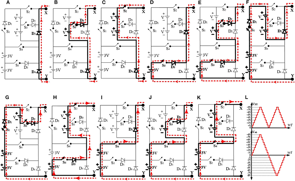
Figure 3. The all possible voltage levels of the level generation circuit: (A) VXY=0; (B) VXY = +V; (C) VXY = +2V; (D) VXY = +3V; (E) VXY = +4V; (F) VXY = +4V; (G) VXY = +5V; (H) VXY = +5V; (I) VXY = +6V; (J) VXY = +7V; (K) VXY = +8V; (L) synthesis of the output voltage of the seventeen level inverter.
Various Modes of Operation of Level Generation Circuit
The modes of operation of the level generation circuit are discussed below:
Mode-0: During this mode of operation the all the switches of the level generation circuit are turned OFF. The current will flow through the diodes D2 and D4, as shown in Figure 3A. The terminals X, Y of the level generation circuit are shorted through D2, D4. Hence the voltage across the level generation circuit is zero (i.e., VXY = 0). The current path during this mode of operation is indicated through the dotted line as shown in Figure 3A.
Mode-1: In this mode of operation the power switch S3 of the level generation circuit is turned ON. The current will flow through the D4, S3, and D4 as shown in Figure 3B. The terminals X, Y of the level generation circuit experience a voltage of “V” though S3, D3, and D4. Hence the voltage across level generation circuit is +V (i.e., VXY = +V). The current path during this mode of operation is indicated through the dotted line as shown in Figure 3B.
Mode-2: During this mode of operation the power switch S2 of the level generation circuit is turned ON. The current will flow through the D4, S2 as shown in Figure 3C. The terminals X, Y of the level generation circuit experience a voltage of “2 V” though S2 and D4. Hence the voltage across the level generation circuit is +2 V (i.e., VXY = +2 V). The current path during this mode of operation is indicated through the dotted line as shown in Figure 3C.
Mode-3: In this mode of operation the power switch S5 of the level generation circuit is turned ON. The current will flow through S5, D2, and D5 as shown in Figure 3D. The terminals X, Y of the level generation circuit experience a voltage of “3 V” though S5, D2, and D5. Hence the voltage across the level generation circuit is +3 V (i.e., VXY = +3 V). The current path during this mode of operation is indicated through the dotted line as shown in Figure 3D.
Mode-4: During this mode of operation the power switches S5 and S3 of the level generation circuit are turned ON. The current will flow through the S5, D5, S3, and D3 as shown in Figure 3E.
The terminals X, Y of the level generation circuit experience a voltage of “4 V” though S5, D5, S3, and D3. Hence the voltage across the level generation circuit is +4 V (i.e., VXY = +4 V). The current path during this mode of operation is indicated through the dotted line as shown in Figure 3E.
Mode-5: In this mode of operation the power switch S1 of the level generation circuit is turned ON. The current will flow through the S1, D1, and D2 as shown in Figure 3F. The terminals X, Y of the level generation circuit experience a voltage of “4 V” though S1, D1, and D2. Hence the voltage across the level generation circuit is +4 V (i.e., VXY = +4 V). The current path during this mode of operation is indicated through the dotted line as shown in Figure 3F.
Mode-6: During this mode of operation the power switches S1 and S3 of the level generation circuit are turned ON. The current will flow through the S1, D1, S3, and D3 as shown in Figure 3G. The terminals X, Y of the level generation circuit experience a voltage of “5 V” though S1, D1, S3, and D3. Hence the voltage across the level generation circuit is +5 V (i.e., VXY = +5 V). The current path during this mode of operation is indicated through the dotted line as shown in Figure 3G.
Mode-7: In this mode of operation the power switches S5 and S2 of the level generation circuit are turned ON. The current will flow through the S5, D5, and S2 as shown in Figure 3H. The terminals X, Y of the level generation circuit experience a voltage of “5 V” though S5, D5, and S2. Hence the voltage across the level generation circuit is +5 V (i.e., VXY = +5 V). The current path during this mode of operation is indicated through the dotted line as shown in Figure 3H.
Mode-8: During this mode of operation the power switch S4 of the level generation circuit is turned ON. The current will flow through the S4 and D2 as shown in Figure 3I. The terminals X, Y of the level generation circuit experience a voltage of “6 V” though S4 and D2. Hence the voltage across the level generation circuit is +6V (i.e., VXY = +6 V). The current path during this mode of operation is indicated through the dotted line as shown in Figure 3I.
Mode-9: In this mode of operation the power switches S4 and S3 of the level generation circuit are turned ON. The current will flow through the S4, S3, and D3 as shown in Figure 3J. The terminals X, Y of the level generation circuit experience a voltage of “7 V” through S4, S3, and D3. Hence the voltage across the level generation circuit is +7 V (i.e., VXY = +7 V). The current path during this mode of operation is indicated through the dotted line as shown in Figure 3J.
Mode-10: During this mode of operation the power switches S4 and S2 of the level generation circuit are turned ON. The current will flow through the S4 and S2 as shown in Figure 3K. The terminals X, Y of the level generation circuit experience a voltage of “8V” though S4 and S2. Hence the voltage across the level generation circuit is +8V (i.e., VXY = +8V). The current path during this mode of operation is indicated through the dotted line as shown in Figure 3K.
The nine voltage levels obtained from the level generation circuit are used to obtain the seventeen voltage levels by using the polarity changer circuit, as shown in Figure 3L.
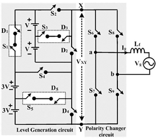
The proposed seventeen level inverter topology can be made bi-directional by replacing unidirectional devices (D1-D5) with controlled power switches. The proposed configuration of the bi-directional seventeen level inverter is shown in Figure 4.
Proposed Pulse Width Modulation Strategy
This section discusses the proposed pulse width modulation (PWM) strategy, the control strategy of the grid-connected seventeen level inverter topology.
Proposed PWM Strategy
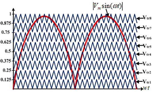
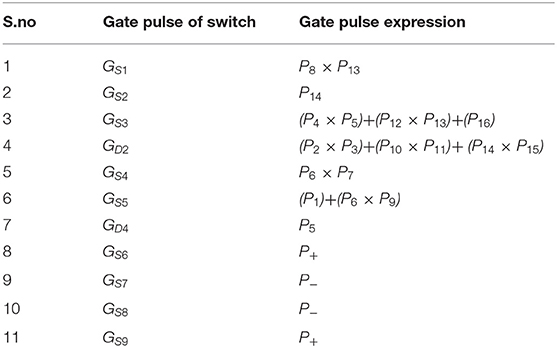
To control the output voltage and generate the seventeen voltage levels, a PWM strategy has been proposed along with its modulation logic. The Figures 5, 6A show the PWM strategy and proposed modulation logic of inverter. In this PWM strategy, a reference waveform (|Vm sinwt|) is compared with the eight carrier waveforms (VC1-VC8) to generate signals P1-P15, as shown in Figures 5, 6A. These signals P1-P15 are modified to obtain the gate pulses for the switches S1-S9 and D1-D5. The obtained expressions for the gate pulses of all switches are given in Table 2.
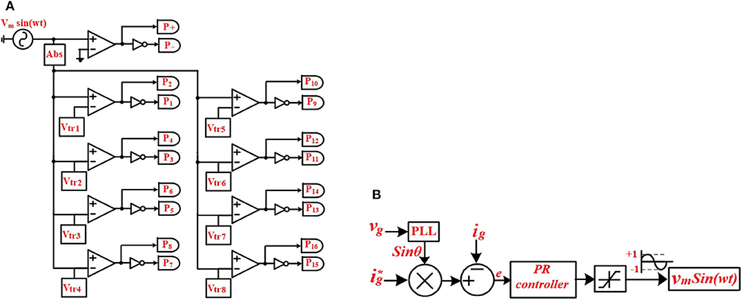
Figure 6. The modulation and control strategies for proposed inverter topology; (A) proposed modulation logic; (B) current control strategy for the grid-connected seventeen level inverter (She et al., 2014).
The Current Control Strategy for the Grid-Connected Seventeen Level Inverter
Figure 6B shows the current control strategy, which is used to control the current feeding into the grid (Lee et al., 2009). In this control strategy, the grid current (ig) is compared with the reference grid current (sinθ) which gives the error signal (e) as output. Here, is the peak amplitude of reference current, and sinθ is obtained from the PLL. The error signal is sent through the proportional resonant (PR) controller which generates the modulating wave Vm(sinwt). This modulating wave is used to generate reference waveform |Vm(sinwt)|. This reference waveform is used to generate the gate pulses for all the switches by using the proposed modulation strategy shown in Figures 5, 6A. The PR-controller's transfer function is given as:
The PR controller is designed by considering the phase margin as 500 and maximum permissible steady-state error of 0.1% of the rated current. The designed values of the PR controller are given as:
Kp = 0.4; Ki = 15; ωcut = 20 rad/sec and ω = 2 × π × 50 rad/sec.
Comparison of the Proposed Seventeen Level Inverter Topology With the Existing MLI Topologies
The proposed seventeen level inverter and bi-directional seventeen level inverter topologies are compared with the existing seventeen level inverter topologies. The proposed inverter topologies require fewer input DC sources, power devices, and lesser requirement of the number of drive signals which reduces the size, cost of the system, and increases the reliability of the system. In addition to that, the total standing voltage (TSV) of high-frequency switches are smaller compared to the existing MLI topologies (given in Table 3). Thus, the proposed inverter topologies incur lower switching losses. The efficiencies of proposed seventeen level inverter topology and bi-directional seventeen level inverter topologies are calculated to be 97 and 96.5%, respectively.

Table 3. The comparison of proposed seventeen level inverter topology with the existing MLI topologies.
The detailed comparison of the proposed seventeen level inverter topology with the existing seventeen level inverter topologies is given in Table 3. From Table 3, it can be observed that the proposed inverter topology doesn't have the reactive power capability even though it uses a lesser number of power devices. However, this issue can be tackled by using the proposed bi-directional inverter topology.
The Extension of Proposed 1-ϕ Seventeen Level Inverter Topology to n-Level
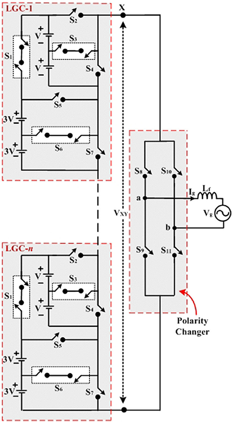
There is a possibility to extend the proposed 1-ϕ seventeen level inverter to higher levels by adding the level generation circuits (LGC) in a cascaded fashion as shown in Figure 7. This is possible due to the modularity of proposed inverter topology, which supports the extension for n-levels. For example, the cascaded connection of level generation circuits (LGC1 and LGC2) generates voltage levels +16, +15 V,…+V, and 0 in the output voltage (VXY). Thus, the +16, +15 V,…+V and 0 voltage levels in the obtained voltages of VXY are used to generate ±16, ±15, ±14, ±13, ±12 V,…. ±V and 0 output voltage Vab associated with the polarity changer. Figure 7 shows the cascaded connection of level generation circuits of LGC1 and LGC2. In this manner, the n-level MLI can be realized by cascading the level generation circuits LGC1, LGC1,…LGC(n−1)/16 in series. The number of level generation circuits (NLGC), DC sources (NDC), switches (Ns), diodes (ND), and total power devices (NPD) required for obtaining n-levels are given by the following equations:
where n = 17, 33, 49, … and NLGC = 1, 2, 3, ….
Extension of Proposed 1-ϕ Seventeen Level Inverter for 3-ϕ Application
The possible extension of the proposed 1-ϕ seventeen level inverter topology for 3-ϕ application is shown in Figure 8. It consists of a total of four sets of DC sources (three V and one 3 V) and 12 controlled switches, nine bi-directional switches. In this 3-ϕ topology, the three legs share a common DC source (two 3 V) which minimizes the required DC sources' count.
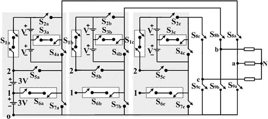
Figure 8. The extended 3-ϕ seventeen level inverter topology (All the nodes marked '1' are connected, similarly all nodes marked '2' are connected).
Simulation Results
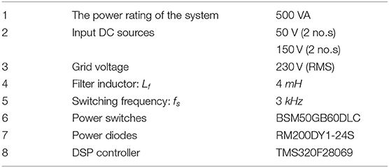
The proposed grid-connected 1-ϕ seventeen level inverter topology is simulated for a power rating of 500 W at a switching frequency of 3 kHz. The MATLAB/Simulink environment is used for the simulation studies. The considered values of two sets of input DC sources are 50 and 150 V. To filter the high-frequency harmonics the filter inductor (Lf) is chosen as 4 mH. The simulated waveforms of the voltage across the level generation circuit (VXY) are shown in Figure 9A. It consists of nine voltage levels 0, 50, 100, 150, 200, 250, 300, 350, and 400 V. By using these nine voltage levels, seventeen voltage levels (0, ±50, ±100, ±150, ±200, ±250, ±300, ±350, and ±400 V) are generated at the output of polarity changer circuit (i.e., output voltage Vab) as shown in Figure 9B. The waveforms of grid voltage and current are also shown in Figure 9C. It can be observed from Figure 9C that the proposed inverter topology is feeding high quality of current into the grid because of the presence of multi-levels in the output voltage. Further, the proposed grid connected inverter topology is simulated at lagging power factor of 0.9 and corresponding waveforms of the output voltage, grid voltage and current are shown in Figure 9D. The waveforms of the current through two sets of input DC source two V and two 3 V (i.e., I1, I2, I3, and I4) are also shown in Figure 9E. The parameters used for the simulation studies are given in Table 4.
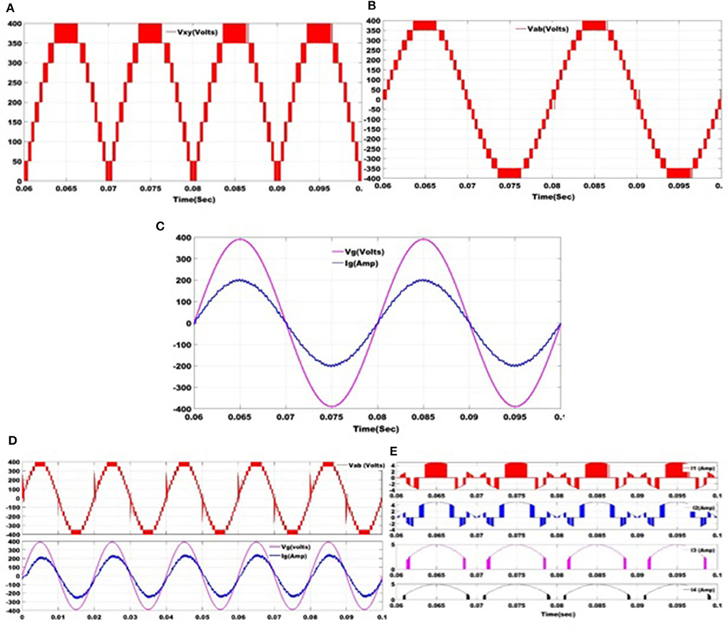
Figure 9. The simulated waveforms of the grid connected seventeen level inverter topology; (A) output voltage of the level generation circuit (VXY); (B) output voltage (Vab); (C) voltage across the grid and current through the grid (Grid current is scaled up 70 times to fit into the graph); (D) output voltage (Vab), voltage across the grid and current through the grid for non UPF (Grid current is scaled up 70 times to fit into the graph); (E) current through input DC sources I1, I2, I3, and I4 (Input currents are scaled up two times to fit into the graph).
Further, the proposed bi-directional seventeen level inverter topology is also verified through simulations for a 500 VA grid-connected system. The simulated waveforms of the voltage across the level generation circuit, output voltage (Vab), the voltage across the grid, and current through the grid at a power factor of 0.95 are shown in Figures 10A–C, respectively. It can be observed from Figure 10C that the proposed bi-directional inverter can feed a nice quality of power into the grid at THD of 2.1% due to the presence of a higher number of levels in the output voltage. The waveforms of the current through two sets of input DC source two V and two 3 V (i.e., I1, I2, I3, and I4) are also shown in Figure 10D.
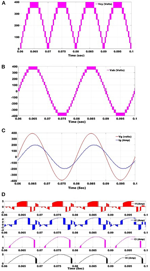
Figure 10. The simulated waveforms of the grid connected bi-directional seventeen level inverter topology at power factor of 0.95; (A) output voltage of the level generation circuit (VXY); (B) output voltage (Vab); (C) voltage across the grid and current through the grid (Grid current is scaled up 70 times to fit into the graph); (D) current through input DC sources I1, I2, I3, and I4 (Input currents are scaled up two times to fit into the graph).
Experimental Results
The proposed seventeen level inverter topology is tested for grid-connected for a power rating of 500 W at switching frequency of 3 kHz on a laboratory prototype (shown in Figure 11A). Table 4 shows the parameters used for the study of the proposed seventeen level inverter topology for the grid-connected system. The experimental waveforms of the output voltage of the level generation circuit (VXY) and inverter output voltage (Vab) are shown in Figure 11B. Further, the experimental waveforms current though the grid and voltage across the grid at unity power factor are also shown in Figure 11C.
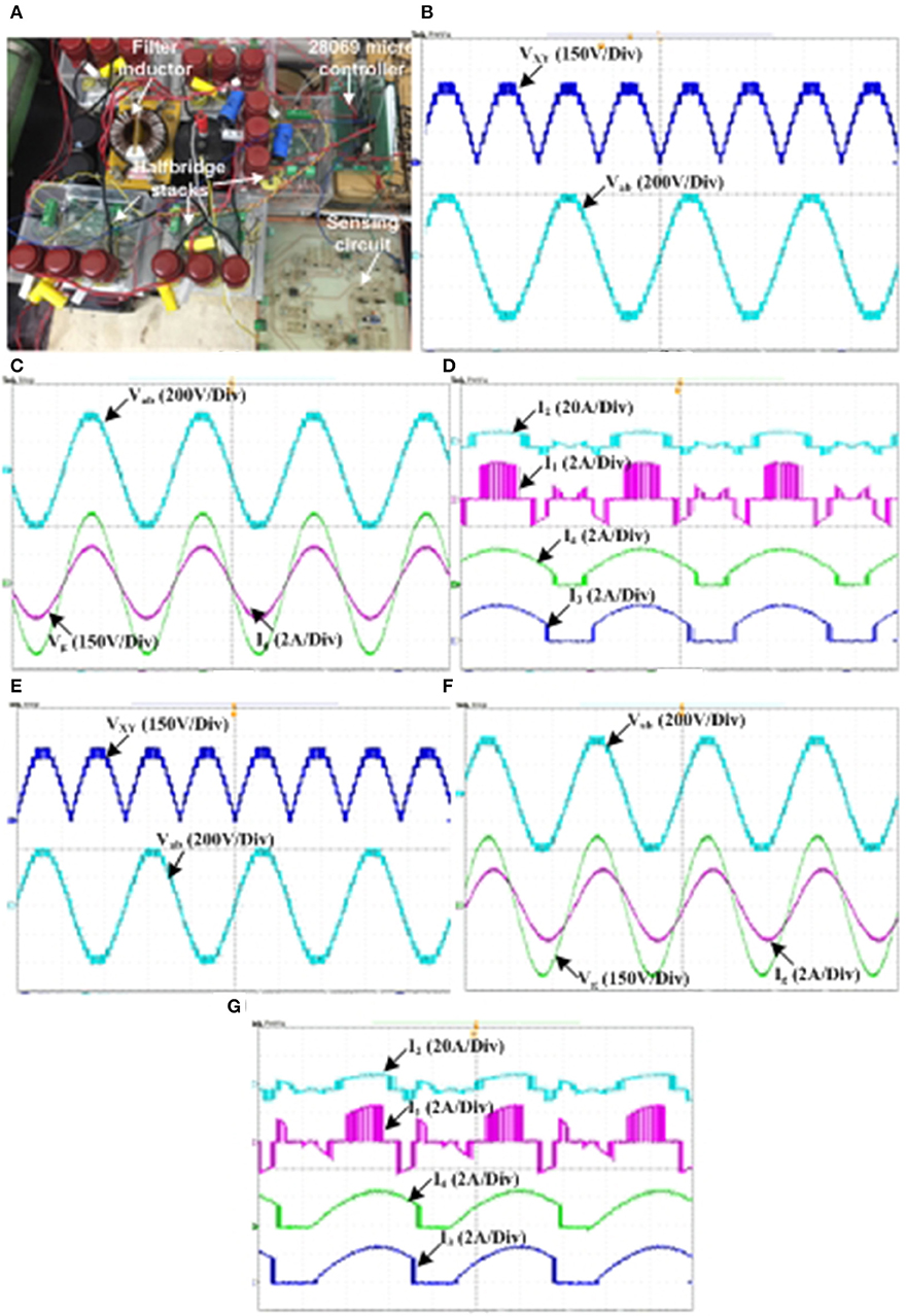
Figure 11. The experimental waveforms of the grid connected seventeen level inverter topology; (A) experimental setup of the grid-connected system; (B) the output voltage of the level generation circuit (VXY) and inverter output voltage (Vab); (C) the grid voltage (Vg) and current through the grid (Ig); (D) the current through the input DC sources (I1, I2, I3, and I4); (E) the output voltage of the level generation circuit (VXY) and inverter output voltage (Vab); (F) The grid voltage (Vg) and current through the grid (Ig); (G) the current through the input DC sources (I1, I2, I3, and I4).
Figure 11D shows the waveforms of the current through the two sets of the input DC sources (I1, I2, I3, and I4). It can be observed from Figure 11C that the inverter output voltage contains seventeen voltage levels and feeds good quality of current into the grid.
Further, the proposed bi-directional seventeen level inverter also tested for grid-connected application at 500 VA power rating. The experimental waveforms level generation circuit output voltage (VXY), inverter output voltage (Vab), grid voltage (Vg), grid current (Ig), and currents through the input DC sources at a power factor of 0.95 are shown in Figures 11E–G. The proposed bi-directional seventeen level inverter also feeds good quality of power into the grid with THD of 2.1%.
Conclusions
This paper has presented a new seventeen level inverter topology for single-phase grid-connected applications. The main advantage of proposed inverter topology is the reduced number of power components. Due to fewer power components, a compact system can be realized. Further, a comparison of the proposed seventeen level inverter topology with the existing MLIs is presented which shows the major advantages of the proposed configuration. The proposed seventeen level inverter has lower conduction losses because at maximum only five switches conduct in any mode of operation. Further, the bi-directional operation of the proposed topology is also presented. The possible 3- ϕ extension of the proposed 1-ϕ seventeen level inverter is also discussed and its extension for higher levels is also investigated. The proposed 1-ϕ seventeen level inverter and bi-directional seventeen level inverters are able to feed high-quality power into the grid with a current THD of 2.36 and 2.1% respectively. The proposed seventeen level inverter topology and its bi-directional operation also validated through experimental results and all the results are presented in the paper which shows the effectiveness of the proposed work.
Data Availability Statement
The raw data supporting the conclusions of this article will be made available by the authors, without undue reservation, to any qualified researcher.
Author Contributions
PC and VA: substantial contributions to the conception or design of the work, or the acquisition, analysis, or interpretation of data for the work. AA-D: drafting the work or revising it critically for important intellectual content. All authors contributed to the article and approved the submitted version.
Funding
This work was supported in part by Advanced Power and Energy Centre (APEC) at Khalifa University, Abu Dhabi, UAE.
Conflict of Interest
The authors declare that the research was conducted in the absence of any commercial or financial relationships that could be construed as a potential conflict of interest.
References
Ahmadi, D., and Wang, J. (2014). Online selective harmonic compensation and power generation with distributed energy resources. IEEE Trans. Power Electr. 29, 3738–3747. doi: 10.1109/TPEL.2013.2278253
Babaei, E., Alilu, S., and Laali, S. (2014a). A new general topology for cascaded multilevel inverters with a reduced number of components based on developed H-bridge. IEEE Trans. Industrial Electr. 61, 3932–3939. doi: 10.1109/TIE.2013.2286561
Babaei, E., and Hosseini, S. H. (2009). New cascaded multilevel inverter topology with the minimum number of switches. Elsevier J. Energy Conv. Manag. 50, 2761–2767. doi: 10.1016/j.enconman.2009.06.032
Babaei, E., Kangarlu, M. F., and Sabahi, M. (2014b). Extended multilevel converters: an attempt to reduce the number of independent DC voltage sources in cascaded multilevel converters. IET Power Electr. 7, 157–166. doi: 10.1049/iet-pel.2013.0057
Babaei, E., Laali, S., and Alilu, S. (2014c). Cascaded multilevel inverter with a series connection of novel H-bridge basic units. IEEE Trans. Industrial Electr. 61, 6664–6671. doi: 10.1109/TIE.2014.2316264
Chattopadhyay, S. K., and Chakraborty, C. (2014). A new multilevel inverter topology with self-balancing level doubling network. IEEE Trans. Industrial Electr. 61, 4622–4631. doi: 10.1109/TIE.2013.2290751
Das, M., and Agarwal, V. (2016). Design and analysis of a high-efficiency dc-dc converter with soft switching capability for renewable energy applications requiring high voltage gain. IEEE Trans. Industrial Electr. 63, 2936–2944. doi: 10.1109/TIE.2016.2515565
Duarte, J. L., Hendrix, M., and Simoes, M. G. (2007). Three-port bidirectional converter for hybrid fuel cell systems. IEEE Trans. Power Electr. 22, 480–487. doi: 10.1109/TPEL.2006.889928
Essakiappan, S., Krishnamoorthy, H. S., Enjeti, P., Balog, R. S., and Ahmed, S. (2015). Multilevel medium-frequency link inverter for utility-scale photovoltaic integration. IEEE Trans. Power Electr. 30, 3674–3684. doi: 10.1109/TPEL.2014.2350978
Farhadi Kangarlu, M., and Babaei, E. (2013). Cross-switched multilevel inverter: an innovative topology. IET Power Electr. 6, 642–651. doi: 10.1049/iet-pel.2012.0265
Gupta, K. K., and Jain, S. (2012). Topology for multilevel inverters to attain the maximum number of levels from given DC sources. IET Power Electr. 5, 435–446. doi: 10.1049/iet-pel.2011.0178
Gupta, K. K., Ranjan, A., Bhatnagar, P., Sahu, K. L., and Jain, S. (2016). Multilevel inverter topologies with reduced device count: a review. IEEE Trans. Power Electr. 31, 135–151. doi: 10.1109/TPEL.2015.2405012
Lai, YS., and Shyu, F. S. (2002). Topology for hybrid multilevel inverter. IEEE Proc. Electric Power Appl. 149, 449–458. doi: 10.1049/ip-epa:20020480
Lee, S. J., Bae, H. S., and Cho, B. H. (2009). “Modelling and control of the single-phase photovoltaic grid-connected cascaded H-bridge multilevel inverter,” in IEEE Conference on Energy Conversion Congress and Exposition (ECCE) (San Jose, CA: IEEE), 43–47.
Lezana, P., Rodriguez, J., and Oyarzun, D. A. (2008). Cascaded multilevel inverter with regeneration capability and reduced number of switches. IEEE Trans. Industrial Electr. 55, 1059–1066. doi: 10.1109/TIE.2008.917095
Liu, D., and Li, H. (2006). A ZVS bi-directional DC-DC converter for multiple energy storage elements. IEEE Trans. Power Electr. 21, 1513–1517. doi: 10.1109/TPEL.2006.882450
Mahato, B., Majumdar, S., and Jana KC. (2019a). Reduction of power electronic devices in a single-phase generalized multilevel inverter. J Circuits Systems Computers. 29:2050093 doi: 10.1142/S0218126620500930
Mahato, B., Majumdar, S., and Jana, K. C. (2019b). A new and generalized structure of single-phase and three-phase cascaded multilevel inverter with reduced power components. Int. Trans. Electrical Energy Syst. 30:e12187. doi: 10.1002/2050-7038.12187
Majumdar, S., Mahato, B., and Jana, K. C. (2018). Optimum structure-based multi-level inverter with doubling circuit configuration. J Circuits Systems Comput. 28:19501949. doi: 10.1142/S0218126619501949
Majumdar, S., Mahato, B., and Jana, K. C. (2020). Implementation of an optimum reduced components multicell multilevel inverter (MC-MLI) for lower standing voltage. IEEE Trans. Industrial Electr. 67, 2765–2775. doi: 10.1109/TIE.2019.2913812
Mathew, J., Rajeevan, P. P., Mathew, K., Azeez, N. A., and Gopakumar, K. (2013). A multilevel inverter scheme with dodecagonal voltage space vectors based on flying capacitor topology for induction motor drives. IEEE Trans. Power Electr. 28, 516–525. doi: 10.1109/TPEL.2012.2195784
Meynard, T. A., and Foch, H. (1992). Multi-level choppers for high voltage applications. Proc. Eur. Conf. Power Electron. Appl. 2, 45–50. doi: 10.1080/09398368.1992.11463285
Nabae Takahashi, I., and Akagi, H. (1981). A new neutral-point-clamped PWM inverter. IEEE Trans. Industrial Appl. IA−17, 518–23. doi: 10.1109/TIA.1981.4503992
Peng, F. Z., Lai, J. S., McKeever, J. W., and Van Coevering, J. (1996). A multilevel voltage source inverter with separate DC sources for static var generation. IEEE Trans. Industrial Appl. 32, 1130–1138. doi: 10.1109/28.536875
Peng, F. Z., Qian, W., and Cao, D. (2010). “Recent advances in multilevel converter/inverter topologies and applications,” in IEEE International Conference in power electronics (IPEC), 492–501. doi: 10.1109/IPEC.2010.5544625
Phanikumar, C., and Agarwal, V. (2013a). “Single phase 9 level grid-connected inverter for photovoltaic applications,” in 4th IEEE Conference on Power Electronics for Distributed Generation Systems (Arkansas: Rogers), 8–11. doi: 10.1109/PEDG.2013.6785631
Phanikumar, C., and Agarwal, V. (2013b). “Novel self-balancing single phase asymmetric 9 level grid-connected inverter for photovoltaic applications,” in Annual IEEE India Conference (INDICON) on Impact of Engineering on Global Sustainability (Mumbai: IEEE), 2782–7. doi: 10.1109/INDCON.2013.6725887
Raushan, R., Mahato, B., and Jana, K. C. (2016). Comprehensive analysis of a novel three-phase multilevel inverter with the minimum number of switches. IET Power Electr. 9, 1600–1607. doi: 10.1049/iet-pel.2015.0682
Ravi, R., Mahato, B., and Jana, K. C. (2017). Optimum structure of a generalized three-phase reduced switch multilevel inverter. Electric Power Systems Res. 157, 10–19. doi: 10.1016/j.epsr.2017.11.017
Rodriguez, J., Lai, J. S., and Peng, F. Z. (2002). Multilevel inverters: a survey of topologies, controls, and applications. IEEE Trans. Industrial Electr. 49, 724–738. doi: 10.1109/TIE.2002.801052
Samadaei, E., Gholamian, S. A., Sheikholeslami, A., and Adabi, J. (2016). An envelope type (e-type) module: asymmetric multilevel inverters with reduced components. IEEE Trans. Industrial Electr. 63, 7148–7156. doi: 10.1109/TIE.2016.2520913
Sharma, P., and Agarwal, V. (2014). Exact maximum power point tracking of grid-connected partially shaded PV source using current compensation concept. IEEE Trans. Power Electr. 29, 4684–4692. doi: 10.1109/TPEL.2013.2285075
She, X., Huang, A. Q., and Ni, X. (2014). Current sensorless power balance strategy for DC/DC converters in a cascaded multilevel converter based solid state transformer. IEEE Trans. Power Electr. 29, 17–22. doi: 10.1109/TPEL.2013.2256149
Shi, J., Gou, W., Yuan, H., Zhao, T., and Huang, A. Q. (2011). Research on voltage and power balance control for cascaded modular solid-state transformer. IEEE Trans. Power Electr. 26, 1154–1166. doi: 10.1109/TPEL.2011.2106803
Sinha Das, M. K., and Jana, K. C. (2019). Control of asymmetrical cascaded multilevel inverter for a grid-connected photovoltaic system. IET Renew. Power Generation. 13, 1456–1465. doi: 10.1049/iet-rpg.2018.5230
Sinha, A., Jana, K. C., and Das, M. K. (2019). Control strategy of PV-fed, grid-interfaced, seven-level T-type MLI for distributed power generation. IET Power Electr. 12, 3208–3219. doi: 10.1049/iet-pel.2019.0379
Sochor, P., and Akagi, H. Theoretical comparison in energy-balancing capability between star- delta-configured modular multilevel cascade inverters for utility-scale photovoltaic systems. IEEE Trans. Power Electr. (2016). 31, 1980–1992. doi: 10.1109/TPEL.2015.2442261
Tao, H., Kotsopoules, A., Duarte, J. L., and Hendrix, M. A. M. (2006). Family of multiport bidirectional DC-DC converters. IEEE Proc. Electric Power Appl. 153, 451–458. doi: 10.1049/ip-epa:20050362
Vahedi, H., Labbé P. A., and Al-Haddad, K. (2016). Sensor-less five-level packed u-cell (PUC5) inverter operating in stand-alone and grid-connected modes. IEEE Trans. Industrial Informatics. 12, 361–370. doi: 10.1109/TII.2016.2578183
Yuan, X. (2014). A set of multilevel modular medium-voltage high power converters for 10-MW wind turbines. IEEE Trans. Sustain Energy. 5, 524–534. doi: 10.1109/TSTE.2013.2297178
Zare (2008). Firuz Power Electronics Education Electronic-Book. Brisbane, QLD: School of Engineering Systems, Queensland University of Technology.
Keywords: multilevel inverter, seventeen level inverter, level-shifted modulation strategy, level generation circuit, polarity changer circuit
Citation: Chamarthi PK, Agarwal V and Al-Durra A (2020) A New 1-ϕ, Seventeen Level Inverter Topology With Less Number of Power Devices for Renewable Energy Application. Front. Energy Res. 8:131. doi: 10.3389/fenrg.2020.00131
Received: 05 February 2020; Accepted: 28 May 2020;
Published: 24 July 2020.
Edited by:
Sudhakar Natarajan, VIT University, IndiaReviewed by:
Bidyut Mahato, Indian Institute of Technology Dhanbad, IndiaKarthik Balasubramanian, Independent Researcher, Singapore, Singapore
Copyright © 2020 Chamarthi, Agarwal and Al-Durra. This is an open-access article distributed under the terms of the Creative Commons Attribution License (CC BY). The use, distribution or reproduction in other forums is permitted, provided the original author(s) and the copyright owner(s) are credited and that the original publication in this journal is cited, in accordance with accepted academic practice. No use, distribution or reproduction is permitted which does not comply with these terms.
*Correspondence: Phani Kumar Chamarthi, cGhhbmlrdW1hcmVlZUBnbWFpbC5jb20=
 Phani Kumar Chamarthi
 Vivek Agarwal2
 Ahmed Al-Durra