- 1Beamline Department, Pohang Accelerator Laboratory, POSTECH, Pohang, South Korea
- 2Advanced Photonics Research Institute, GIST, Gwangju, South Korea
- 3Department of Physics, University of Seoul, Seoul, South Korea
- 4Surface Technology Division, Materials Center for Energy Convergence, Korea Institute of Materials Science, Changwon, South Korea
- 5School of Chemical Engineering and Australian Institute for Bioengineering and Nanotechnology, The University of Queensland, Brisbane, QLD, Australia
- 6Divison of Materials Science, Nara Institute of Science and Technology, Nara, Japan
Understanding the defect structure in organic-inorganic hybrid perovskite material (OHP) is a crucial role to explain several physical properties such as material stability, energy band, carrier mobility, and so on. In the solar-cell applications using OHP, finding, understanding, and controlling defects is essential to making a more advanced device with high efficiency and stability. Naturally, we need to find, understand, and control the possible defects in OHP. However, the defect research field in OHP material is just beginning now. In this short review, we will explore the kinds of defects and their effects on OHP.
Why We Need to See Defects in Organic-Inorganic Hybrid Perovskite?
Recently, the National Renewable Energy Laboratory (NREL) in the USA has announced a new world record for power conversion efficiency (PCE) in organic-inorganic hybrid perovskite (OHP) based solar-cell (Figure 1; Berhe et al., 2016; Ono and Qi, 2016, 2018). It was 22.7% with a significant competition with CdTe (22.1%), CIGS (22.6%), and Si (25.4%; Ono and Qi, 2018). It is surprising that the fast development for only 9 years is now coming true to be a compelling candidate instead of the current commercial material, silicon. Many researchers are considering the end of the PCE race and now need to focus more on the fundamental viewpoint. The research goal in OHP-based solar-cells has been clear: “Make an OHP-based solar-cell with easy/cheap fabrication, high PCE, and stable performance.” The result of this goal looks very successful now.
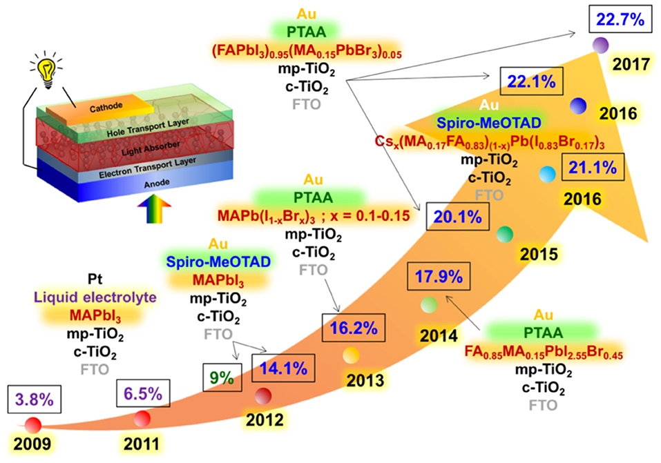
Figure 1. Historical review of PCE with different HTLs and OHPs. Copyright 2018 IOP Publishing. [Reprinted with permission from Ono and Qi (2018)].
After the first report from the Miyasaka group in 2009 (Kojima et al., 2009), researchers were trying many engineering works with the change of (1) hole transport layer (sprio-MeOTAD→PTAA), (2) organic cation parts (CH3: MA→NH2CH = : FA, or their mixtures), and (3) halides (Cl, Br, I, or their mixtures) to obtain a high PCE and device stability (In the case of electron transport layers, currently, it looks almost fixed with mesoporous-TiO2/compact-TiO2; Figure 1).
These changes to improve the PCE were performed mainly after understanding the physical properties from defects in the formed OHP film and at each interface of hole transport layer (HTL)/OHP/electron transport layer (ETL). Because these defects caused low PCE and high device instability generally. In the case of the I− migration and MA disordering of MAPbI3-based solar-cells, for instance, it manifested the hysteresis behavior in I-V measurement and the degradation of OHP (Figure 2; Walsh, 2015; Berhe et al., 2016; Ono and Qi, 2018). The I− migration (also, it is the same calling, vacancy migration) is a kind of delocalized defect which causes a change of physical property and material instability (Peng et al., 2018). So, if we can avoid or minimize the migration of halide anions and MA disordering, device performance will be more stable without any material degradation. The current engineering works such as the mixtures of MA/FA and I/Br originate to minimize these defect behaviors.
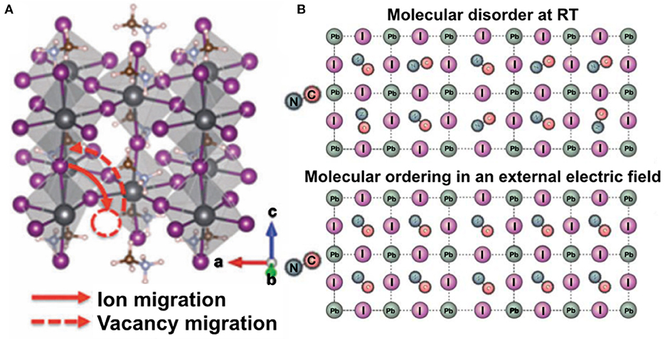
Figure 2. (A) Schematic of I−/vacancy migration in OHP and (B) MA molecular disordering. [Reprinted with permission from Walsh (2015) and Berhe et al. (2016)].
The weakness of OHP material is well-known when it exposed to air (especially, water) during and after fabrication. Many researchers are trying to overcome this weakness which is the critical factor to decrease the device lifetime (Figure 3A). The fast degradation due to contamination by water and oxygen is a severe problem for the use of OHP material for a commercial product (Figure 3B). From the defect viewpoint, it is due to a different element-incorporated structure such as contamination and impurity. In fact, many researchers have tried to solve the material weakness using some ideas. The use of optimized hole transport layers with the functions of air-protection and reasonable hole mobility was a good approach (Jung et al., 2015; Yang et al., 2015; Kranthiraja et al., 2017). Also the change of the organic or inorganic parts in the OHP structure to improve the material weakness were tried (Rehman et al., 2015; Li et al., 2018). From the understanding of the contamination mechanism, we could suggest and prove a new structure in the OHP-based solar-cell application.
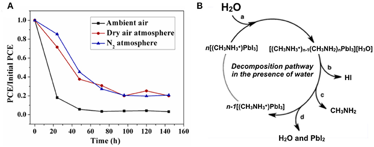
Figure 3. (A) The degradation of power conversion efficiency in OHP-based solar-cell device and (B) The chemical degradation in the water incorporation with OHP material. [Reprinted with permission from Frost et al. (2014) and Zhou et al. (2014)].
Researchers tried to change the metal cation from Pb to Sn because Pb is an environmental poison and cannot be accepted in current industries. However, it turns out to be dramatically unstable material during the process of device fabrication Hao et al., 2014; Noel et al., 2014; Jung et al., 2016a; Shao et al., 2017; Song et al., 2017. That is the reason why researchers cannot avoid the Pb cation in OHP material (Please, think about the recent structure. The active material of the 22.7% PCE cell is (FAPbI3)0.95(MA0.15PbBr3)0.05. We still cannot avoid the use of Pb element; Figure 1). Recently, Lee et al. have revealed the reason of material instability in Sn-based perovskite which was originated from the surface chemical instability (Lee et al., 2018). From this finding, we can assume naturally that if we can deposit a protection layer on the surface of Sn-based perovskite thin film, it could obtain non-degradation because the material instability induces from only the surface. This approach also offers one of the right solutions by understanding a defect structure.
From these short historical reviews with the defect viewpoint, we confirm that the understanding of the defect structure in OHP material is an effective approach to explain and improve physical properties such as material stability, well-defined energy band, and high carrier mobility. In the OHP-based solar-cell application, especially, the controlling of defects is essential to make a more improved solar-cell device with high efficiency and long life-time. In fact, we know these research approaches are standard in semiconductor industries, i.e., we already used the defect effect such as n-/p-type doping to control the carriers by adding a donor or acceptor level in the bandgap. In the case of OHP-based solar-cell applications, naturally, we need to understand and control possible defects. In this short review, we will look at the types of defects based on traditional defect physics and examine their effects in OHP-based solar-cell applications. Furthermore, we would like to suggest the one research field in fundamental defect structure for future research agenda in OHP material because defect studies for the recent material of the best efficiency devices such as (FAPbI3)0.95(MA0.15PbBr3)0.05 are not finished yet.
Intrinsic (or Native) Defects: Vacancy, Schottky/Frenkel Defects, and Delocalized Defect
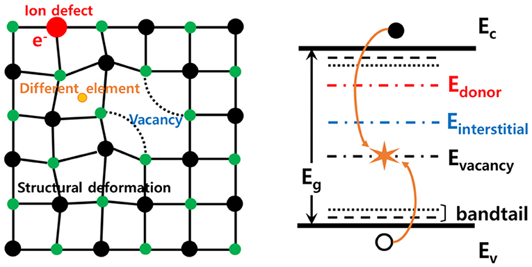
In semiconductor fundamentals such as phonons, band structure, electronic transport, and optical properties are essential (McCluskey and Haller, 2012). To start understanding defects, we need to define the kinds of defects such as the intrinsic or native (the lattice vacancy, the interstitial host atom, the Schottky, and Frenkel defects) and extrinsic defects (impurities). Because these representative defects originating from vacancies are one of the critical reasons to cause a pinned defect energy level (deep or shallow levels) in the energy gap (Figure 4; Drabold and Estreicher, 2007; McCluskey and Haller, 2012). Even the local native defects can induce the variation of crystal phase transition temperature (Dobrovolsky et al., 2017; Ma et al., 2018). It means that if we can classify all kinds of defects in OHP, we can explain important physical properties in OHP-based solar-cell applications.
In the case of intrinsic (or native) defects in OHP material, several theoretical works with an ideal single crystal were performed. Kim et al. at 2014 focused on the Schottky and the Frenkel defects such as PbI2/CH3NH3I and Pb/I/CH3NH3 vacancies, respectively (Kim et al., 2014). Schottky defects in OHP, such as PbI2 and CH3NH3I vacancy, do not make a trap state within the band gap, which can reduce carrier lifetime. However, elemental defects derived from Frenkel defects, such as Pb, I, and CH3NH3 vacancies, form shallow levels near the band edges to play the role of unintentional doping sources (Figure 5). The absence of gap states from intrinsic defects of MAPbI3 can be ascribed to the ionic bonding from organic–inorganic hybridization. Besides, Vogel et al. claimed that the role of lead vacancies in OHP causes the spin specific trap state at near valence band (Figure 6; Vogel et al., 2017).
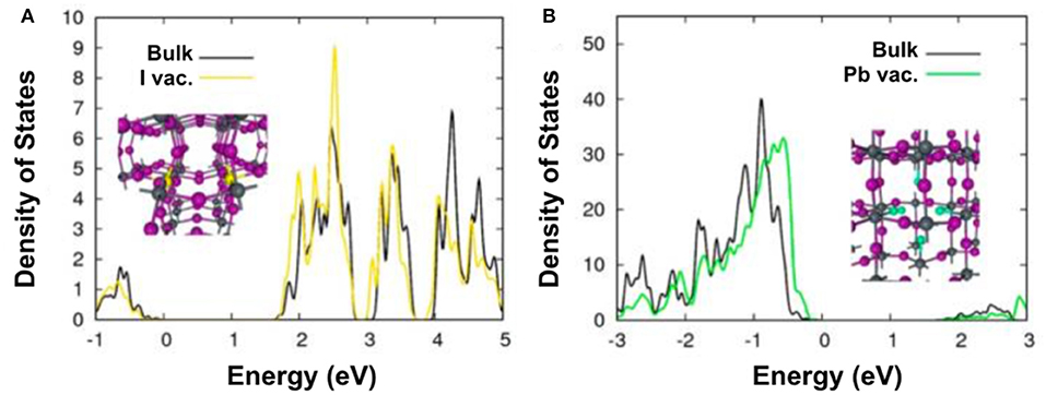
Figure 5. The density of states (DOS) with (A) I and (B) Pb vacancies in comparison of bulk. The changes of DOS are observed in I and Pb vacancies. [Reprinted with permission from Kim et al. (2014)].

Figure 6. DOS in MAPbI3, VPb+2, and VPb singlet. The trap state in VPb+2 appears. [Reprinted with permission from Vogel et al. (2017)].
Recently, Liu and Yam performed the first-principle calculation of intrinsic defects in formamidinium lead triiodide (FAPbI3) perovskite material (Liu and Yam, 2018). From their calculations, we can find that FA-related defects have low formation energies and create deep levels in the bandgap. We understand these deep levels will lead to increase an electron-hole recombination ratio and reduce a non-equilibrium lifetime. They suggest a growing environment of I-rich to avoid defects.
In the case of photovoltaic material, “defect-tolerance” is essential because there are no deep state levels and only shallow state levels (Brandt et al., 2015, 2017). Several reports are showing MAPbX3 is a kind of defect-tolerant semiconductor which is expected to (a) form relatively few intrinsic or structural defects under high-throughput, low-temperature processing conditions, and/or (b) the extrinsic, intrinsic, or structural defects that form a very minimal effect on carrier mobility and lifetime (Figure 7; Brandt et al., 2017). From these postulates, they could explain why organic-inorganic hybrid perovskite, MAPbX3, can have good carrier mobility and long lifetime.
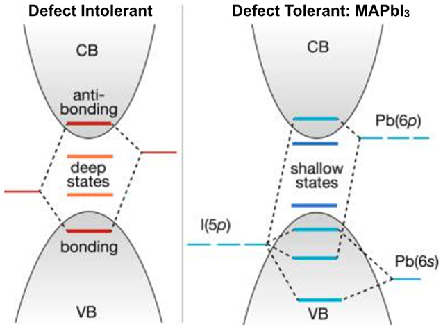
Figure 7. Electronic structure (conduction and valence bands with defect levels) of typical semiconductor with the direct band gap (left) and MAPbI3 (right). [Reprinted with permission from Brandt et al. (2017)].
All these theoretical works mentioned mainly the localized defects in real space (The deep level generally refers to a defect wave function that is localized in real space; McCluskey and Haller, 2012). Although, OHP thin film has many kinds of localized defects, interestingly, these defects do not affect the carrier mobility and long lifetime. That reason is why OHP is possible to be a powerful candidate for future solar-cell material.
On the other hand, OHP has also the delocalized defect such as the transport of charged ionic defect, I− migration (Frost and Walsh, 2016; Yuan and Huang, 2016). Frost and Walsh found several specific internal motions of MAPbI3 and FAPbI3 such as (1) molecular rotation-libration in the cuboctahedral cavity, (2) drift and diffusion of large electron and hole polarons, and (3) transport of charged ionic defects. In their report, the focus is the dynamic behavior of OHPs, which has been linked to the performance, degradation, and unusual physics of these materials and their associated devices. In the defect viewpoint, the I− migration is a kind of delocalized defect which is reflected in a hysteresis effect in I-V measurements of the solar-cell device using OHP material. During the device working, this defect is exploring in all areas of the device with changing the device property in real-time. Recently, Peng et al. have reported Br− migration, which was a kind of delocalized defect (Peng et al., 2018). And, they consider that OHP is a mixed electronic/ionic semiconductor. These delocalized defects, such as the migration of halide anion element, cause the different transport properties in the time evolution on a device. We believe this viewpoint is very important to understand OHP material. If our viewpoint for OHP is “Inorganic-based semiconductor with organic defect,” OHP is just a weaker material than a Si-based semiconductor with the unexpected and uncontrolled physical property. However, if we can focus on defect physics in OHP material, we can lead a new material physics such as a mixed defect state with both localized and delocalized defects. Even if we can control these defects, we can find a new physics and its related application from this viewpoint.
Extrinsic Defects: Trap State and Molecular Defect at Grain Boundary
In this section, we will focus on the defect at the grain boundary in OHP thin film. Heretofore, we have explored defects mainly in a single crystal. For solar-cell applications, in general, OHP thin films with “polycrystalline phase” are used. The polycrystalline makes a grain boundary with a different structure such as structural deformation and stoichiometry-broken. This structural deformation can make a trap state to affect to carrier mobility. In the case of OHP, as a result, the effect of trap states at the grain boundary is minimal or of no influence on the carrier mobility.
Sherkar et al. investigated the attributes of the primary trap-assisted recombination channels; namely, grain boundaries (GBs) and interfaces, and their correlation to ionic defects in existing OHP-based solar-cells (Sherkar et al., 2017). They found that despite the presence of traps at grain boundaries (GBs), their neutral (when filled with photogenerated charges) disposition along with the long-lived nature of holes leads to the high performance of OHP-based solar-cells (Figure 8). The sign (if charged or neutral when filled) of traps is of little importance in efficient solar cells with compact morphologies (fused grain boundaries, low trap density). They found a direct correlation between the density of trap states, the density of mobile ions, and the degree of hysteresis observed in the current–voltage (J–V) characteristics.

Figure 8. Schematic of trap state behaviors at the grain boundary in (A) typical inorganic (poly-Si, CdTe) and (B) OHP-based solar-cells. [Reprinted with permission from Sherkar et al. (2017)].
Obviously, the grain boundary caused the lower charge-carrier mobility (Herz, 2017). Grain size is clearly shown with a dependence of limiting of carrier mobility (Please, see the table 1 in Herz, 2017). However, Shan and Saidi found that (1) the grain boundary region is the sink for most of the native-point defects under different synthesis conditions and (2) crystalline MAPbI3 does not have deep transition levels (Figure 9; Shan and Saidi, 2017). From their calculations, I-poor conditions at the grain boundary are most preferable for the synthesis of MAPbI3 to have defects with electronically benign character. In all of the studies for the defect at the grain boundary in OHP, interestingly, the defect effect is not serious.
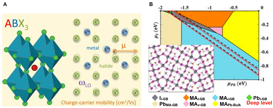
Figure 9. Schematic of (A) charge-carrier and (B) sink at the grain boundary in OHP. [Reprinted with permission from Herz (2017) and Shan and Saidi (2017)].
Recently, Jung et al. reported the presence of CH3NH2 neutral species at the grain boundary in the MAPbI3 thin film (Jung et al., 2016b). From the experiment of near-edge x-ray absorption of fine structure, two important pieces of information were found:(1) CH3NH2 molecular defect at the grain boundary and (2) the different surface chemical states with C=C and C*-M bondings (Figure 10). If the CH3NH2 molecular defect is located at the grain boundary, the structural deformation originated from this defect will have a high possibility to be a deep trap state. From their calculation of density of states, however, there is no trap state, and even no bandgap. This result is similar with Sherkar's finding (Sherkar et al., 2017).
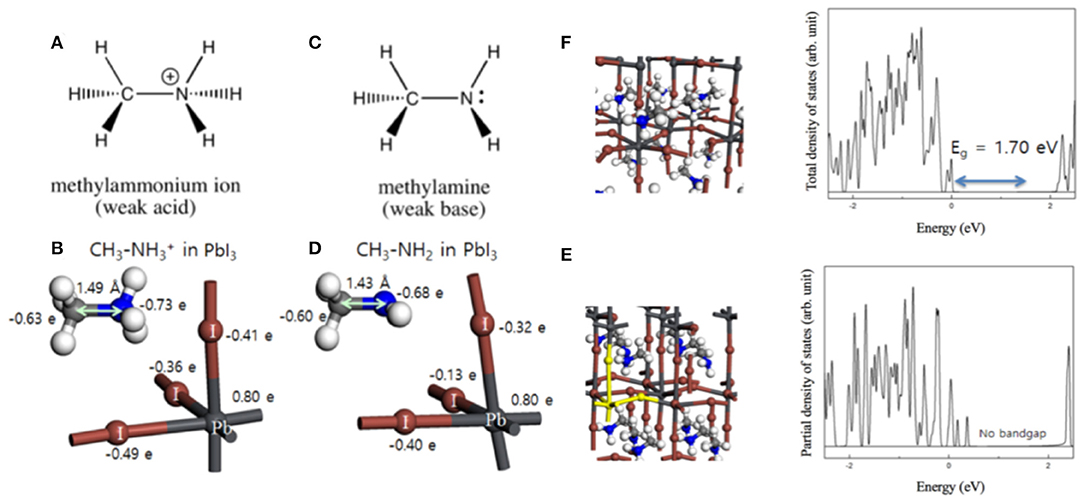
Figure 10. Electron configurations in (A,B) CH3 cation and (C,D) CH3NH2 molecule in perovskite structure. The perovskite structure is distorted with CH3NH2 neutral molecule. The DOS calculation for the bandgap of (F) CH3NH3PbI3 and (E) CH3NH2PbI3. The CH3NH2PbI3 has no bandgap. [Reprinted with permission from Jung et al. (2016b)].
Moreover, they mentioned this molecular defect could be removed from OHP thin film after the post-annealing process. Unfortunately, they did not focus on the different surface chemical states. We do not know the origin of C=C and C*-M bondings such as from the solvent remaining or the symmetry-broken on the surface. However, we can assume that these different chemical states originate from a solvent remaining after spin-casting because several reports using the vacuum-evaporated methods could not find any different chemical state in the measurement of x-ray photoelectron spectroscopy (Hamill et al., 2018). In any case, these different chemical states on the surface can cause a structural deformation at the interface after the deposition of a hole-transport layer. We believe that this requires additional study.
Summary and Outlook: We Need to Study Defect for Current OHP Research
We have explored defects in OHP, which is a powerful candidate for future solar-cells. Vacancy in OHP does not create the deep energy level in the bandgap. Moreover, the most defect energy level is a kind of shallow level to naturally improve energy distribution for device performance. However, this vacancy in OHP-based solar-cell devices causes a halide migration, which generates the degradation of device performance. To avoid the vacancy problem, many researchers tried to use a mixed organohalide perovskite such as (FAPbI3)0.95(MA0.15PbBr3)0.05 and have obtained the best PCE over 22%. However, the defect study is not fully finished for this OHP material.
Many theoretical works were performed with only ideal single crystal. These works were instrumental initially in understanding defects in OHP. To go ahead to the next step for a real device, however, we should focus on a polycrystalline thin film with “grain boundary.” In this case, theoretical works are not enough to understand defect structures at the grain boundary. In this review, the authors suggest several measurements to understand (1) atomic structure, (2) electronic structure of defects, and (3) their trap states at the grain boundary using Grazing-angle Incident X-ray Diffraction (GIXD; Park et al., 2018), high-resolution Photoelectron Spectroscopy (PES; Kojima et al., 2018) with synchrotron radiation, and Field-Effect Thermally-Stimulated-Current (FE-TSC; Kojima et al., 2018), respectively. GIXD will provide a finely detailed structure of polycrystalline OHP thin film from the surface to bulk included with the grain boundary. We can find defect structures and their locations. PES measurement will provide exact chemical states in a thin film with the grain boundary. If a different chemical state such as a broken-stoichiometry and different element from the grain boundary, PES measurement can detect. Finally, FE-TSC measurement can offer trap states with their energy levels and depths. It will be understood with a relationship between trap states at the grain boundary and carrier mobility.
In general, researchers are interested in defects when they found some unexpected physical properties. The most important thing in the defect study is “understanding” and “controlling.” Controlled defects can improve a device performance dramatically and make a new physical property which can start a new research application. In solar-cell application, generally, the energy levels originated from defects are not good in the viewpoint of device performance. In optoelectronics such as a light-emitting diode, however, the control of defects including the creation of new energy level is important to diverse light in various energy ranges. It means the defect study is essential to all of viewpoints. Lastly, we strongly suggest the defect study for recent proposed OHP materials.
Author Contributions
M-CJ designed and supervised. YL, IM and M-CJ wrote the manuscript. All authors discussed all of concepts and contents.
Funding
Japan: JSPS KAKENHI Grant No. 17K05033. Republic of Korea: NRF Basic Science Research Program and Creative Materials Discovery Program No. NRF-2015R1C1A2A01054543, NRF-2015R1D1A1A01059958, NRF-2018R1D1A1B07042814, and NRF-2018M3D1A1056688. Australia: Australian Research Council through DP (DP170104379) and DECRA (DE180101253) programs.
Conflict of Interest Statement
The authors declare that the research was conducted in the absence of any commercial or financial relationships that could be construed as a potential conflict of interest.
Acknowledgments
The authors thank Associate Professor Leigh McDowell from the Nara Institute of Science and Technology (NAIST) for valuable suggestions in revising the manuscript.
References
Berhe, T. A., Su, W.-N., Chen, C.-H., Pan, C.-J., Cheng, J.-H., Chen, H.-M., et al. (2016). Organometal halide perovskite solar cells: degradation and stability. Energy Environ. Sci. 9, 323–356. doi: 10.1039/C5EE02733K
Brandt, R. E., Poindexter, J. R., Gorai, P., Kurchin, R. C., Hoye, R. L. Z., Nienhaus, L., et al. (2017). Searching for “defect-tolerant” photovoltaic materials: combined theoretical and experimental screening. Chem. Mater. 29, 4667–4674. doi: 10.1021/acs.chemmater.6b05496
Brandt, R. E., Stevanović, V., Ginley, D. S., and Buonassisi, T. (2015). Identifying defect-tolerant semiconductors with high minority-carrier lifetimes: beyond hybrid lead halide perovskites. MRS Commun. 5, 265–275. doi: 10.1557/mrc.2015.26
Dobrovolsky, A., Merdasa, A., Unger, E. L., Yartsev, A., and Scheblykin, I. G. (2017). Defect-induced local variation of crystal phase transition temperature in metal-halide perovskites. Nat. Commun. 8:34. doi: 10.1038/s41467-017-00058-w
Drabold, D. A., and Estreicher, S. (2007). Theory of Defects in Semiconductors. Berlin; Heidelberg: Springer-Verlag. Available online at: //www.springer.com/gp/book/9783540334002 (Accessed June 13, 2018).
Frost, J. M., Butler, K. T., Brivio, F., Hendon, C. H., van Schilfgaarde, M., and Walsh, A. (2014). Atomistic origins of high-performance in hybrid halide perovskite solar cells. Nano Lett. 14, 2584–2590. doi: 10.1021/nl500390f
Frost, J. M., and Walsh, A. (2016). What is moving in hybrid halide perovskite solar cells? Acc. Chem. Res. 49, 528–535. doi: 10.1021/acs.accounts.5b00431
Hamill, J. C., Schwartz, J., and Loo, Y.-L. (2018). Influence of solvent coordination on hybrid organic–inorganic perovskite formation. ACS Energy Lett. 3, 92–97. doi: 10.1021/acsenergylett.7b01057
Hao, F., Stoumpos, C. C., Cao, D. H., Chang, R. P. H., and Kanatzidis, M. G. (2014). Lead-free solid-state organic-inorganic halide perovskite solar cells. Nat. Photonics 8, 489–494. doi: 10.1038/nphoton.2014.82
Herz, L. M. (2017). Charge-carrier mobilities in metal halide perovskites: fundamental mechanisms and limits. ACS Energy Lett. 2, 1539–1548. doi: 10.1021/acsenergylett.7b,00276
Jung, M. C., Raga, S. R., Ono, L. K., and Qi, Y. (2015). Substantial improvement of perovskite solar cells stability by pinhole-free hole transport layer with doping engineering. Sci. Rep. 5, 9863–9865. doi: 10.1038/srep09863
Jung, M. C., Raga, S. R., and Qi, Y. (2016a). Properties and solar cell applications of Pb-free perovskite films formed by vapor deposition. RSC Adv. 6, 2819–2825. doi: 10.1039/C5RA21291J
Jung, M. C, Lee, Y. M., Lee, H. K., Park, J., Raga, S. R., et al. (2016b). The presence of CH 3NH 2neutral species in organometal halide perovskite films. Appl. Phys. Lett. 108:073901. doi: 10.1063/1.4941994
Kim, J., Lee, S.-H., Lee, J. H., and Hong, K.-H. (2014). The role of intrinsic defects in methylammonium lead iodide perovskite. J. Phys. Chem. Lett. 5, 1312–1317. doi: 10.1021/jz500370k
Kojima, A., Teshima, K., Shirai, Y., and Miyasaka, T. (2009). Organometal halide perovskites as visible-light sensitizers for photovoltaic cells. J. Am. Chem. Soc. 131, 6050–6051. doi: 10.1021/ja809598r
Kojima, H., Nakagawa, M., Abe, R., Fujiwara, F., Yakiyama, Y., Sakurai, H., et al. (2018). Thermoelectric and thermal transport properties in sumanene crystals. Chem. Lett. 47, 524–527. doi: 10.1246/cl.171210
Kranthiraja, K., Gunasekar, K., Kim, H., Cho, A.-N., Park, N.-G., Kim, S., et al. (2017). High-performance long-term-stable dopant-free perovskite solar cells and additive-free organic solar cells by employing newly designed multirole π-conjugated polymers. Adv. Mater. 29:1700183. doi: 10.1002/adma.201700183
Lee, Y. M., Park, J., Yu, B. D., Hong, S., Jung, M.-C., and Nakamura, M. (2018). Surface instability of Sn-based hybrid perovskite thin film, CH3NH3SnI3: the origin of its material instability. J. Phys. Chem. Lett. 9, 2293–2297. doi: 10.1021/acs.jpclett.8b00494
Li, B., Zhang, Y., Fu, L., Yu, T., Zhou, S., Zhang, L., et al. (2018). Surface passivation engineering strategy to fully-inorganic cubic CsPbI 3 perovskites for high-performance solar cells. Nat. Commun. 9:1076. doi: 10.1038/s41467-018-03169-0
Liu, N., and Yam, C. (2018). First-principles study of intrinsic defects in formamidinium lead triiodide perovskite solar cell absorbers. Phys. Chem. Chem. Phys. 20, 6800–6804. doi: 10.1039/C8CP00280K
Ma, C., Shen, D., Qing, J., Ng, T.-W., Lo, M.-F., and Lee, C.-S. (2018). Heat treatment for regenerating degraded low-dimensional perovskite solar cells. ACS Appl. Mater. Interfaces 10, 4860–4865. doi: 10.1021/acsami.7b15059
McCluskey, M. D., and Haller, E. E. (2012). Dopants and Defects in Semiconductors. CRC Press. Available online at: https://www.crcpress.com/Dopants-and-Defects-in-Semiconductors/McCluskey-Haller/p/book/9781466553804 (Accessed June 13, 2018).
Noel, N. K., Stranks, S. D., Abate, A., Wehrenfennig, C., Guarnera, S., Haghighirad, A.-A., et al. (2014). Lead-free organic–inorganic tin halide perovskites for photovoltaic applications. Energy Env. Sci. 7, 3061–3068. doi: 10.1039/C4EE01076K
Ono, L. K., and Qi, Y. (2016). Surface and interface aspects of organometal halide perovskite materials and solar cells. J. Phys. Chem. Lett. 7, 4764–4794. doi: 10.1021/acs.jpclett.6b01951
Ono, L. K., and Qi, Y. (2018). Research progress on organic–inorganic halide perovskite materials and solar cells. J. Phys. Appl. Phys. 51:093001. doi: 10.1088/1361-6463/aaa727
Park, B., Kedem, N., Kulbak, M., Lee, D. Y., Yang, W. S., Jeon, N. J., et al. (2018). Understanding how excess lead iodide precursor improves halide perovskite solar cell performance. Nat. Commun. 9:3301. doi: 10.1038/s41467-018-05583-w
Peng, W., Aranda, C., Bakr, O. M., Garcia-Belmonte, G., Bisquert, J., and Guerrero, A. (2018). Quantification of ionic diffusion in lead halide perovskite single crystals. ACS Energy Lett. 3, 1477–1481. doi: 10.1021/acsenergylett.8b00641
Rehman, W., Milot, R. L., Eperon, G. E., Wehrenfennig, C., Boland, J. L., Snaith, H. J., et al. (2015). Charge-carrier dynamics and mobilities in formamidinium lead mixed-halide perovskites. Adv. Mater. 27, 7938–7944. doi: 10.1002/adma.201502969
Shan, W., and Saidi, W. A. (2017). Segregation of native defects to the grain boundaries in methylammonium lead iodide perovskite. J. Phys. Chem. Lett. 8, 5935–5942. doi: 10.1021/acs.jpclett.7b02727
Shao, S., Liu, J., Portale, G., Fang, H. H., Blake, G. R., ten Brink, G. H., et al. (2017). Highly reproducible Sn-based hybrid perovskite solar cells with 9% efficiency. Adv. Energy Mater. 7:1702019. doi: 10.1002/aenm.201702019
Sherkar, T. S., Momblona, C., Gil-Escrig, L., Ávila, J., Sessolo, M., Bolink, H. J., et al. (2017). Recombination in perovskite solar cells: significance of grain boundaries, interface traps, and defect ions. ACS Energy Lett. 2, 1214–1222. doi: 10.1021/acsenergylett.7b00236
Song, T.-B., Yokoyama, T., Aramaki, S., and Kanatzidis, M. G. (2017). Performance enhancement of lead-free tin-based perovskite solar cells with reducing atmosphere-assisted dispersible additive. ACS Energy Lett. 2, 897–903. doi: 10.1021/acsenergylett.7b00171
Vogel, D. J., Inerbaev, T. M., and Kilin, D. S. (2017). Role of lead vacancies for optoelectronic properties of lead-halide perovskites. J. Phys. Chem. C 122, 5216–5226. doi: 10.1021/acs.jpcc.7b05375
Walsh, A. (2015). Principles of chemical bonding and band gap engineering in hybrid organic–inorganic halide perovskites. J. Phys. Chem. C 119, 5755–5760. doi: 10.1021/jp512420b
Yang, W. S., Noh, J. H., Jeon, N. J., Kim, Y. C., Ryu, S., Seo, J., et al. (2015). High-performance photovoltaic perovskite layers fabricated through intramolecular exchange. Science 348, 1234–1237. doi: 10.1126/science.aaa9272
Yuan, Y., and Huang, J. (2016). Ion migration in organometal trihalide perovskite and its impact on photovoltaic efficiency and stability. Acc. Chem. Res. 49, 286–293. doi: 10.1021/acs.accounts.5b00420
Keywords: organic-inorganic hybrid perovskite, thin film, solar-cell, defect, vacancy, Schottky/Frankel defect, delocalized defect, molecular defect
Citation: Lee YM, Maeng I, Park J, Song M, Yun J-H, Jung M-C and Nakamura M (2018) Comprehensive Understanding and Controlling the Defect Structures: An Effective Approach for Organic-Inorganic Hybrid Perovskite-Based Solar-Cell Application. Front. Energy Res. 6:128. doi: 10.3389/fenrg.2018.00128
Received: 06 July 2018; Accepted: 13 November 2018;
Published: 29 November 2018.
Edited by:
Tayebeh Ameri, Universität München, GermanyReviewed by:
Thomas Stergiopoulos, Aristotle University of Thessaloniki, GreeceJie Min, Wuhan University, China
Copyright © 2018 Lee, Maeng, Park, Song, Yun, Jung and Nakamura. This is an open-access article distributed under the terms of the Creative Commons Attribution License (CC BY). The use, distribution or reproduction in other forums is permitted, provided the original author(s) and the copyright owner(s) are credited and that the original publication in this journal is cited, in accordance with accepted academic practice. No use, distribution or reproduction is permitted which does not comply with these terms.
*Correspondence: Min-Cherl Jung, bWNqdW5nQG1zLm5haXN0Lmpw
†These authors have contributed equally to this work
 Young Mi Lee
 Inhee Maeng
 Jinwoo Park
 Myungkwan Song
 Jung-Ho Yun
 Min-Cherl Jung
 Masakazu Nakamura6