 Sheng-Han Su1,2
 Wei-Ting Hsu3Chang-Lung Hsu1
 Chang-Hsiao Chen1
 Ming-Hui Chiu1Yung-Chang Lin4
 Wen-Hao Chang3Kazu Suenaga4
 Jr-Hau He2
 Lain-Jong Li1*
- 1Institute of Atomic and Molecular Sciences, Academia Sinica, Taipei, Taiwan
- 2Department of Electrical Engineering, Graduate Institute of Photonics and Optoelectronics, National Taiwan University, Taipei, Taiwan
- 3Department of Electrophysics, National Chiao Tung University, Hsinchu, Taiwan
- 4National Institute of Advanced Industrial Science and Technology (AIST), Tsukuba, Japan
The electronic and optical properties of transition-metal dichalcogenide (TMD) materials are directly governed by their energy gap; thus, band-gap engineering has become an important topic recently. Theoretical and some experimental results have indicated that these monolayer TMD alloys exhibit direct-gap properties and remain stable at room temperature, making them attractive for optoelectronic applications. Here, we systematically compared the two approaches of forming MoS2xSe2(1–x) monolayer alloys: selenization of MoS2 and sulfurization of MoSe2. The optical energy gap of as-grown chemical vapor deposition MoS2 can be continuously modulated from 1.86 eV (667 nm) to 1.57 eV (790 nm) controllable by the reaction temperature. Spectroscopic and microscopic evidences show that the Mo–S bonds can be replaced by the Mo–Se bonds in a random and homogeneous manner. By contrast, the replacement of Mo–Se by Mo–S does not randomly occur in the MoSe2 lattice, where the reaction preferentially occurs along the crystalline orientation of MoSe2 and thus the MoSe2/MoS2 biphases are easily observed in the alloys, which makes the optical band gap of these alloys distinctly different. Therefore, the selenization of metal disulfide is preferred and the proposed synthetic strategy opens up a simple route to control the atomic structure as well as optical properties of monolayer TMD alloys.
Introduction
Two-dimensional transition-metal dichalcogenide (TMD) monolayers quickly emerge due to their promising properties, including moderate carrier mobility values (Radisavljevic et al., 2011; Kaasbjerg et al., 2012), good bendability, and direct band gaps (Mak et al., 2010; Splendiani et al., 2010; Wang et al., 2012). These advantages could be beneficial to many applications such as low-power electronics (Radisavljevic et al., 2011; Yu et al., 2012; Lin et al., 2013), flexible applications (Pu et al., 2012, 2014), optoelectronic devices (Bernardi et al., 2013; Oriol et al., 2013; Tsai et al., 2013; Zhang et al., 2013; Hsu et al., 2014), and catalysis (Chang et al., 2014). Since the optical responsivity and conversion efficiency at different wavelengths in optoelectronic devices are dominated by the optical band gap of the TMD monolayer, band-gap engineering has become one of the research focuses. It has been reported that the optical band gap of TMD monolayers can be modified by strain engineering (Feng et al., 2012; Lu et al., 2012; Pan and Zhang, 2012; Peelaers and Van de Walle, 2012; Hui et al., 2013) or the formation of heterojunction TMD layers (Ghorbani-Asl et al., 2013). Alternatively, monolayer TMD alloys such as MoxW1-xS2 have been obtained by mechanical exfoliation from the corresponding TMD solid solutions (Chen et al., 2013). The recent breakthrough in the chemical vapor deposition (CVD) growth of MoS2, WSe2, and WS2 monolayers (Lee et al., 2012, 2013; Huang et al., 2014) has stimulated the direct growth of monolayer TMD alloys. Several recent manuscripts have shown that MoS2xSe2(1-x) is obtainable through the gas phase reaction of MoO3 with the mixture of S and Se (Gong et al., 2013; Li et al., 2014; Mann et al., 2014). These preliminary works prove the theoretical prediction that TMD monolayer alloys are stable at room temperature (Jiang, 2012). However, large variations in atomic composition from flakes to flakes are expected owing to the difficulty to precisely control the S and Se vapor diffusion in a CVD furnace. A scalable method to synthesize monolayer TMD alloys with controllable optical energy gaps is still urgently needed for practical applications.
In this contribution, we show that both the CVD-grown molybdenum and tungsten dichalcogenides monolayer flakes can be selenized or sulfurized at high temperatures. The optical band gap of the obtained MoSxSey and WSxSey monolayers ranges from 1.57 to 2.0 eV. Spectroscopic and microscopic results suggest that the replacement of Mo–S by Mo–Se occurs more homogeneously compared to the replacement of Mo–Se by Mo–S. It is suggested that the selenization of metal disulfides is more favorable in the synthetic control of the compositions and optical properties for monolayer TMD alloys.
Materials and Methods
Synthesis of Monolayer TMD
The CVD-grown MoS2, MoSe2, WS2, and WSe2 monolayers were synthesized based on several previous reports (Lee et al., 2012, 2013; Lin et al., 2012; Huang et al., 2014). Taking monolayer MoS2 single crystals as an example, c-plane sapphire (0001) substrates (Tera Xtal Technology Corp.) were first cleaned in a piranha solution [H2SO4/H2O2 (70:30)] at 100°C for 1 h. Substrates were then placed in the center of a 4″ tubular furnace on a quartz holder. The MoO3 powders (0.6 g; Sigma-Aldrich, 99.5%) in an Al2O3 crucible were placed next to the sapphire substrates. The S (Sigma-Aldrich, 99.5%) powders were placed at the upstream position, where the schematic illustration of the growth system was described elsewhere (Zhang et al., 2013). The furnace was first heated to 150°C at 10°C/min rate with 70 sccm Ar at 10 torr and annealed for 20 min, then ramped to 650°C at 25°C/min rate and kept for 20 min. Sulfur was heated separately by heating belt to 170°C when the furnace reached 400°C. After growth, furnace was slowly cooled to room temperature.
Selenization (Sulfurization) Process
The as-grown monolayer MoS2 (MoSe2) and WS2 (WSe2) single crystal flakes were selenized (sulfurized) in a hot-wall furnace at 600, 700, 800, and 900°C. Briefly, as-grown MoS2 (MoSe2) and WS2 (WSe2) monolayers on sapphire were placed in the center of the quartz tube. The selenium (sulfur) powders were placed at the upstream position and heated to 270°C (160°C) with a separate heating belt. The furnace was heated to 600, 700, 800, and 900°C at 30°C/min rate and kept for 2 h for reaction. After selenization (sulfurization), the furnace was slowly cooled to room temperature.
Characterizations
Photoluminescence spectra were performed with a green light (532 nm) laser and 0.9 NA of objective lens (spot size: 0.7 μm). Raman spectra were collected in a NT-MDT confocal Raman microscopic system (laser wavelength 473 nm and laser spot size ~0.5 μm). The Si peak, 520 cm−1, was used as reference for wavenumber calibration. The atomic force microscopy (AFM) images were performed in a Veeco Dimension-Icon system. The transmittance spectra of the MoS2 flakes were obtained using a JASCO-V-670 UV–Vis spectrophotometer. Chemical configurations were determined by X-ray photoelectron spectroscope (XPS, Phi V5000). XPS measurements were performed with an Mg Kα X-ray source on the samples. The energy calibrations were made against the C 1 s peak to eliminate the charging of the sample during analysis.
Results and Discussions
As described in the Section “Materials and Methods,” the triangular monolayer TMD flakes with a lateral size up to several tens of microns can be obtained by our proposed CVD method and it has been adopted by many other groups (Amani et al., 2013; Zhao et al., 2013). In order to tune the electronic structures and optical band gaps of TMD monolayers, we perform the selenization/sulfurization in a hot-wall furnace at various temperatures. The schemes in Figures 1A,D illustrate the experimental set-up for the selenization and sulfurization processes, respectively, where the inlet gas (a mixture of Ar and H2) carries the vaporized selenium or sulfur to the heated MoS2 or MoSe2 flakes. It should be noted that hydrogen gas is required in the process to avoid the oxidation of MoS2 or MoSe2 by residual oxygen or unavoidable oxygen leaking from the environment. Figures 1B,E show the optical micrographs for the as-synthesized MoS2 and MoSe2 on sapphire substrates before selenization or sulfurization. Those for the selenized MoS2 and sulfurized MoSe2 at 800°C are displayed in Figures 1C,F, respectively. There is no obvious change in size and shape of the MoS2 (MoSe2) flakes after selenization (sulfurization). The AFM image for the MoS2 (MoSe2) flakes before and after selenization (sulfurization) at 800°C is shown in inset of each OM image. Note that the slight changes in thickness after selenization or sulfurization are within the AFM measurement errors.
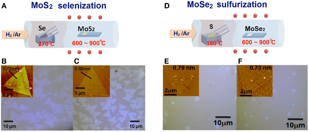
Figure 1. (A,D) Schematic illustration of the experimental set-up for the selenization/sulfurization process, where the inlet gas carries the vaporized selenium (sulfur) to the heated MoS2 (MoSe2) flakes and optical micrographs for the (B,E) as-synthesized MoS2/MoSe2, and (C,F) selenized (sulfurized) MoS2/MoSe2 (at 800°C) on sapphire substrates. AFM images for the MoS2/MoSe2 flakes before and after selenization (sulfurization) (at 800°C) are shown as insets in OM images.
The Raman spectra for the MoS2 (MoSe2) flakes before and after selenization (sulfurization) at different temperatures are shown in Figure 2. No significant changes are observed for the MoS2 (MoSe2) samples after selenization (sulfurization) at 600°C, where the MoS2 (MoSe2) characteristic peaks, 385.6 (286.3) cm−1 for mode and 405.8 (241.1) cm−1 for A1g mode, are predominant in both as-grown and 600°C-reacted samples. As the temperature increases to 700°C, both MoS2 and MoSe2 flakes after respective selenization and sulfurization exhibit several unidentified peaks at around 200–300 cm−1, which are likely attributed to the vibration from the partially selenized Mo–S or sulfurized Mo–Se structures and worth further investigations in the future. When the process is performed at 800°C (750°C), MoS2 (MoSe2) flakes start to be converted to MoSe2 (MoS2), which is evidenced by the presence of the Raman (A1g) and A1g () modes of MoSe2 (MoS2) at 287.1 (383.1) cm−1 and 239.0 (405.4) cm−1, respectively (Tonndorf et al., 2013; Su et al., 2014). It should be mentioned that in Figure 2A, the weak shoulder and unassigned peak occurred at around 249.8 cm−1 for the selenization process, which implies that the quality of MoSe2 is still not perfect. When the selenized temperature of MoS2 reaches 900°C, the perfect A1g and peaks are shown at 242.2 and 289 cm−1. Meanwhile, the shoulder peak completely disappears and no MoS2 feature peaks are observed, indicating the selenization process is successful. On the other hand, the MoSe2 flakes sulfurized at 800 and 900°C exhibit two sharp MoS2 Raman peaks. Hence, we could confirm that both MoS2 and MoSe2 can be successfully converted to each other at a higher process temperature.
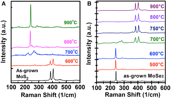
Figure 2. Raman spectra for the (A) MoS2 and (B) MoSe2 flakes before and after selenization/sulfurization at different temperatures are shown.
X-ray photoemission spectroscopy was utilized to characterize the chemical bonding structures of these monolayer flakes. Figure 3 displays the detailed XPS scans for the Mo, S, and Se binding energies for the as-grown MoS2 (MoSe2) and those after selenization (sulfurization), where the magnitude of each profile was normalized for easier comparison. From Figure 3A, the peaks at 232.5 and 229.3 eV represent the Mo 3d3/2 and Mo 3d5/2 binding energies for Mo4+ (Majumdera and Takoudis, 2008). The S 2p1/2 and S 2p3/2 orbital of divalent sulfide ions (S2−) are identified at 163.3 and 162.1 eV (Wang et al., 2013). Moreover, the observation of a doublet peak (232.4 and 235.6 cm−1) indicates the presence of MoO3. For selenization process, a weak doublet peak of Se 3d3/2 (55.3 cm−1) and Se 3d5/2 (54.5 cm−1) binding energy appears even after a low temperature process (600°C), which means that XPS is more sensitive than Raman in the structural characterization for monolayer alloys. As the selenization temperature increases, the doublet peak of Se 3d3/2, Se 3d5/2 becomes more dominant and the binding energy peak of S 2p1/2 and S 2p3/2 gradually disappears. After 900°C selenization, the S characteristic peaks are absent, further confirming that the MoS2 selenization process is successfully completed. Similarly, the results for MoSe2 sulfurization shown in the Figure 3B demonstrate that MoSe2 can be sulfurized to MoS2 at 900°C. Both the selenization and sulfurization processes take effects at the temperature higher than 600°C.
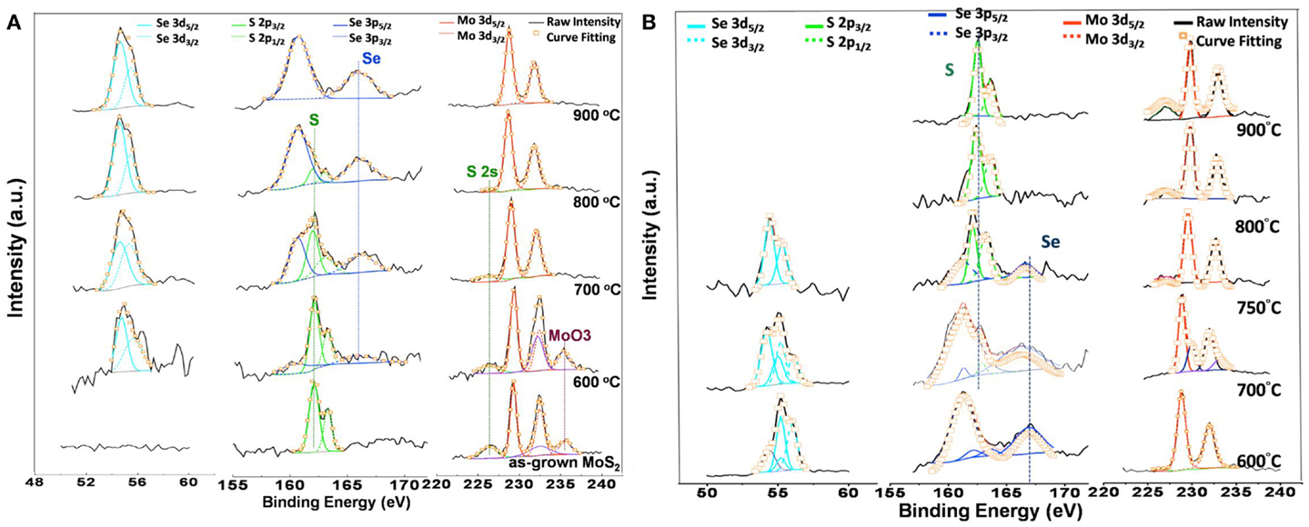
Figure 3. XPS scans for the Mo, S, and Se binding energies for (A) the as-grown MoS2 and those after selenization, and (B) the as-grown MoSe2 and those after sulfurization. The magnitude of each profile was normalized for easier comparison.
We perform the photoluminescence measurements using microscopically focused light (532 nm; spot size: 0.7 μm) to study the optical properties of selenized MoS2. Figure 4A shows the photoluminescence spectra collected for the samples before and after selenization at different temperatures. The emission peak wavelength 667 nm for the MoS2 selenized at 600°C is still pretty similar to the 668 nm peak of the pristine MoS2 samples. The peak wavelength for the sample selenized at 700°C is at 726 nm and the wavelength continues to increase to 768 and 790 nm for the samples selenized at 800 and 900°C, respectively. The emission wavelength (790 nm) for the MoS2 selenized at 900°C is very close to the reported values from 792 nm (Tonndorf et al., 2013) to 800 nm (Kong et al., 2013) for the exfoliated monolayer MoSe2. Figure 4B shows the optical absorption spectrum for these samples. Two distinct absorption peaks at approximately 794.2 and 700.4 nm, identified as A and B excitonic absorptions are observed and these peak positions are consistent with those for exfoliated MoSe2 (Tonndorf et al., 2013). It should be mentioned that A and B excitons are generated by the splitting of valence band due to the spin–orbital splitting effect. It is obvious that MoS2 gradually transforms into MoSe2 from 600 to 900°C. By considering the photoluminescence, absorption spectra, and Raman features, it is suggested that the 900°C selenized sample is close to that of the reported MoSe2 monolayer (Tonndorf et al., 2013). Moreover, we present in Figures 4C,D the energy variation and the spin–orbital splitting vs. selenized temperature. The optical energy gap gradually becomes lower with the temperature, consistent with the PL results. From the absorption peaks, the spin–orbital splitting can be derived as 180 meV for MoS2 and 250 meV for MoSe2. The optical features in Figure 4 are in line with the calculations by Komsa and Krasheninnikov (2012) where the entropic contributions promote the mixing of MoS2 and MoSe2 (Jiang, 2012), which is energetically more preferable over the segregated phases in the mixture even at 300 K. The optical properties of MoSe2 before and after sulfurization are shown in the Figure 5. The emission peak at 804 nm for MoSe2 sulfurized by 600°C is also similar to that of the as-grown MoSe2. The PL peak remains at 809 nm but becomes broader after sulfurization at 700°C, which suggests that the MoSe2 starts to react with S at around 700°C. In clear contrast to the selenization of MoS2, Figures 5A,B show that the PL and absorption features of the MoSe2 suddenly changes to MoS2-like when the sulfurization temperature is equal to or higher than 750°C. The optical band gap of the sulfurized MoSe2 does not seem to be adjustable as those obtained from the selenization of MoS2. The spin–orbital splitting energy with the sulfurization temperature also shows the same behavior.
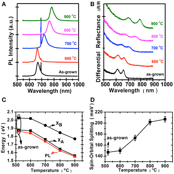
Figure 4. Optical properties of MoS2 selenization are collected for the samples before and after selenization: (A) Photoluminescence spectra, the peak at 694 nm was from the sapphire substrate. (B) Absorption spectra. (C) The optical energy gap of (A,B), exciton, and PL peaks. (D) The spin–orbital splitting derived from the absorption spectra.
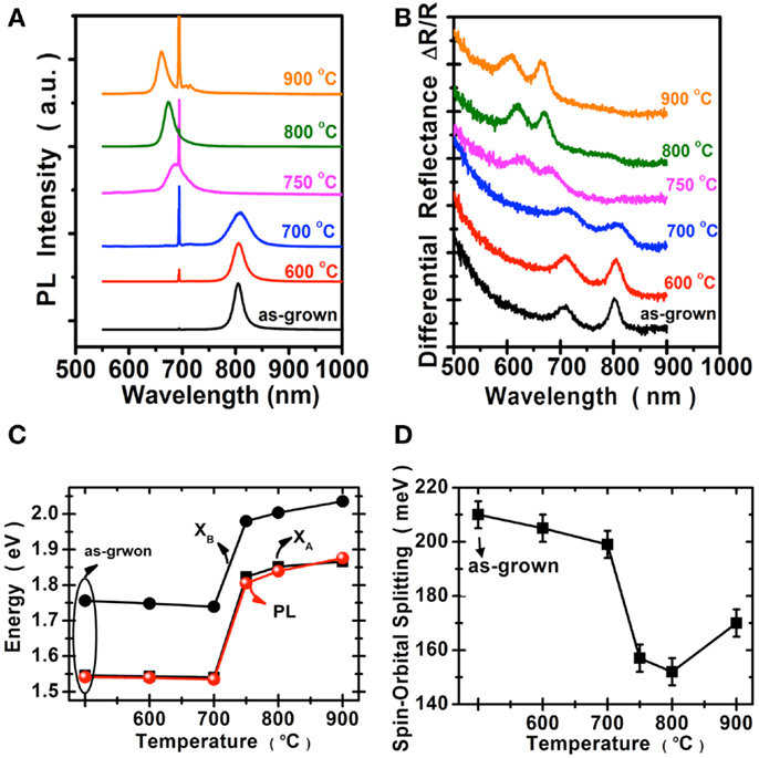
Figure 5. Optical properties of the MoSe2 are collected before and after sulfurization. (A) Photoluminescence spectra, where the peak at 694 nm was from the sapphire substrate. (B) Absorption spectra. (C) The optical energy gap of (A,B), excitons, and PL peaks. (D) The spin–orbital splitting derived from the absorption spectra.
In order to microscopically reveal the homogeneity of the samples, some flakes are selected for visualization under TEM. Figures 6A,B are the MoS2 flakes after selenization at 600 and 700°C, respectively. Both Figures demonstrate that the replacement of S by Se is random and homogeneous in the lattice. It is noted that some replacement occurs at 600°C although the Raman, PL, and absorption spectra do not show pronounced changes as described before. After the MoS2 is selenized at 700°C, large numbers of S2, Se2, and S–Se are identified and the replacement seems to be not only randomly located but also with some identifiable triangle patterns. Since it is generally homogeneous in location, the optical properties can be considered to originate from the MoSxSey alloy. By contrast, Figures 6C–E show the TEM images for the MoSe2 flakes after sulfurization at 700°C. The field is composed of two obvious MoS2 and MoSe2 domains, where MoSSe domains are also found in some areas. In general, the sulfurization seems to preferentially proceed through certain directions, which are related to the crystal orientation. Since theoretical prediction suggests that the mixing of MoS2 and MoSe2 is energetically more preferable over the segregated phases, the formation of biphases is likely due to the kinetic factor. Meanwhile, the preferential formation of biphases in morphology can also explain their distinctly different optical properties, where the PL and absorption peaks are either dominated by MoS2 or MoSe2, depending on the degree of sulfurization.
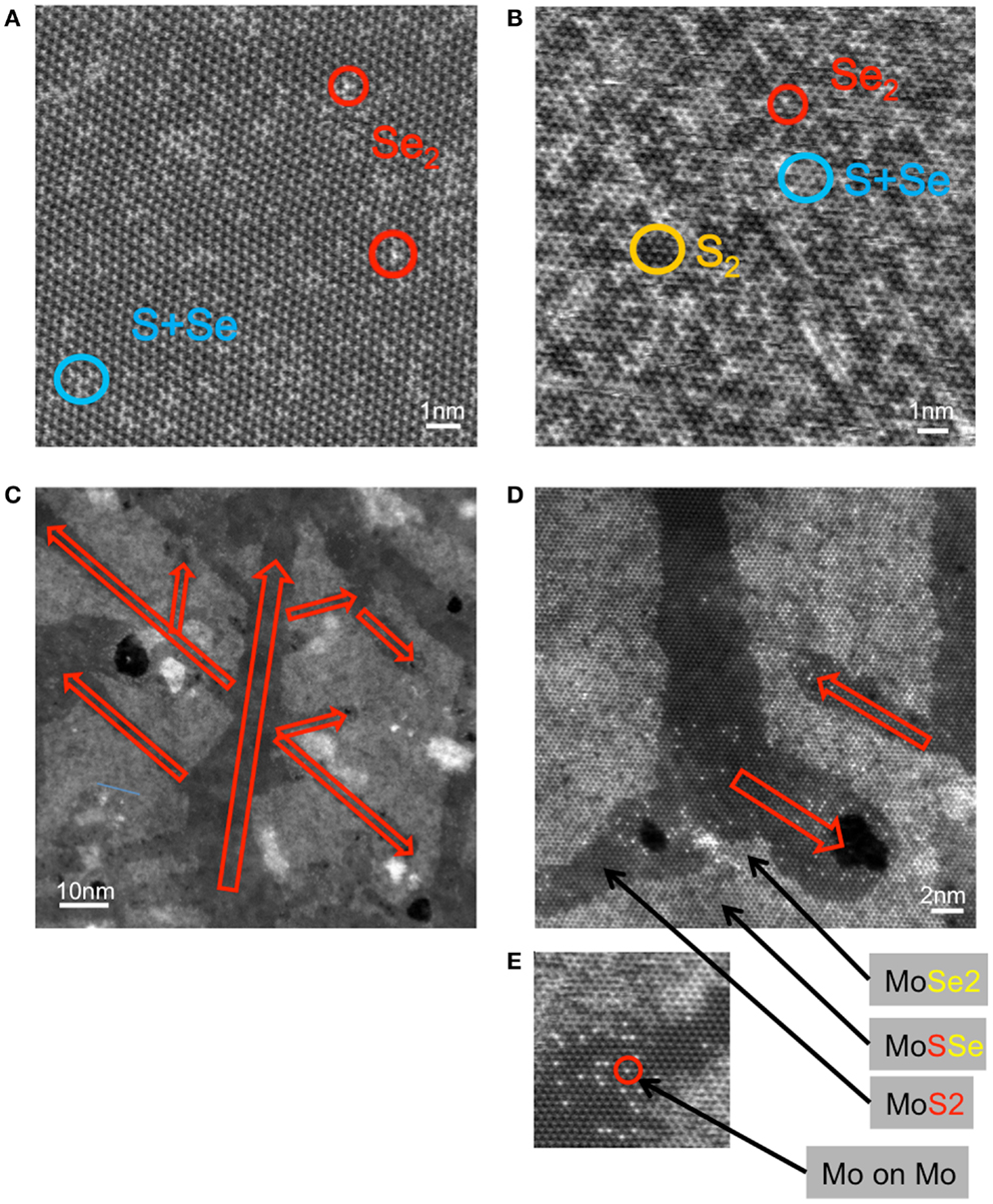
Figure 6. TEM images of the MoS2 flakes selenized at (A) 600°C and (B) 700°C and (C–E) MoSe2 sulfurized at 700°C.
In addition to molybdenum dichalcogenides, the same method has also been utilized to selenize (sulfurize) the WS2 (WSe2) flakes, respectively. Figures 7B,C show the Raman and PL spectra for the WS2 flakes after selenization at various temperatures. Similar to the case of MoS2 selenization, we can see the gradual increase in emission wavelength from 621 to 684 nm when the selenization temperature increases from 600 to 850°C. However, when the temperature reaches 900°C, all the triangular flakes are completely gone, which could be observed in Figure 7A. Hence, it could infer that the thermostability of WS2 is not as good as MoS2. The consistent results are revealed in the Raman spectra in Figure 8B, where the WS2 peaks at 358 and 419 cm−1 gradually disappear and the WSe2 peak at 279 cm−1 becomes pronounced with increasing temperature. On the flip side, WSe2, similar to MoSe2, could be fully and successfully sulfurized. Figure 8A displays the AFM and OM images for the WSe2 flakes before and after sulfurization at 800°C. The Raman spectra in Figure 8B reveal that the WSe2 peaks located at 250 and 260 cm−1 still remain at 700°C. When the temperature reaches 800°C, the Raman peaks from WS2 are dominated, but PL peak is still closer to WSe2 emission. The PL results in Figure 8C suggest that the sample is composed of biphase domains, similar to the previously described sulfurization of MoS2. These suggest that WSe2 starts to but is not yet completely transformed to WS2. Based on the PL results, the sulfurization of WSe2 starts to become pronounced when the temperature is higher than 900°C.
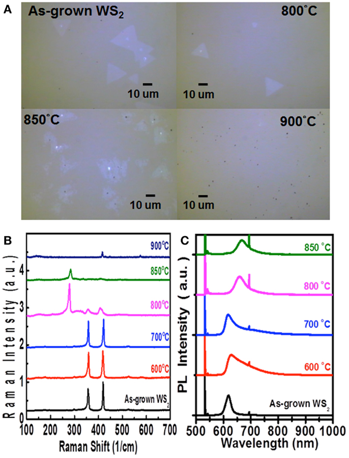
Figure 7. (A) Optical images, (B) Raman spectra, and (C) PL spectra for the WS2 monolayer flakes after selenization at various temperatures are shown.
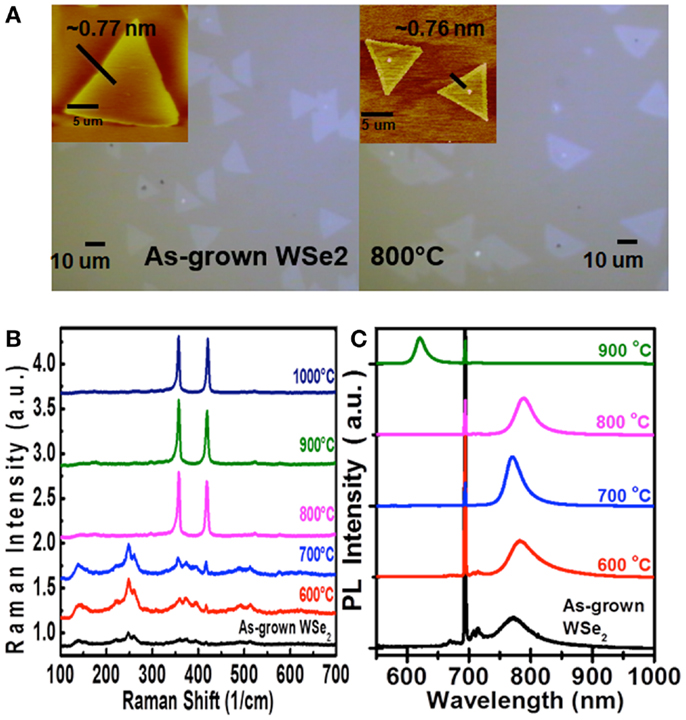
Figure 8. (A) OM and AFM images, (B) Raman spectra, and (C) PL spectra of the WSe2 flakes after sulfurization at various temperatures.
To reveal the chemical composition, we estimate the S content in Figure 9 for each sample by the ratio between Mo–S and (Mo-Se + Mo–S) based on XPS spectra (not shown here). For example, the Mo–S percentage for the as-grown MoS2 and those selenized at 600, 700, 800, and 900°C is 100, 85.8, 26.2, 5, and 0%, respectively. The observed trend strongly agrees the conversion of Mo–S to Mo–Se bonds. The solid line represents the experimental results by Gong et al. (2013) and the dash line is the theoretical results (Kang et al., 2013). It is clearly seen that the experimental optical band gap is larger than the calculated gap. Most importantly, the conversion is governed by the selenization temperature, indicating that the process is thermodynamically controlled. However, due to the presence of biphase domains, the PL peak position vs. S% for MoSe2 sulfurization exhibits distinctly different behavior compared to that for MoS2 selenization.
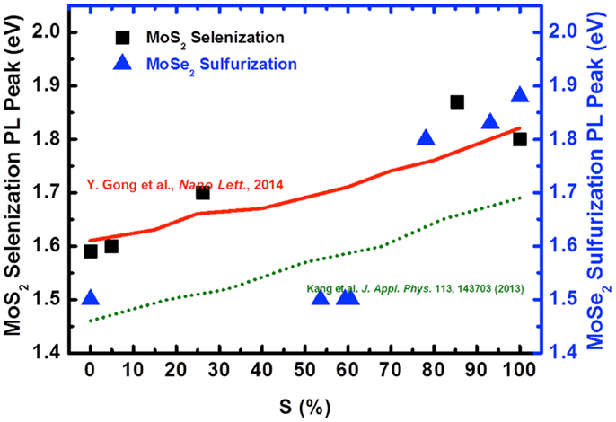
Figure 9. The optical gap of selenization (square symbol) and sulfurization (triangle symbol) with the variation of Sulfur composition is shown. The experimental from Gong et al. (solid line) and theoretical results (dash line) are for references.
Conclusion
In summary, we report that the CVD-grown TMD monolayer flakes can be successfully selenized and sulfurized with a simple and straightforward method. The optical band gap, ranging from 1.57 eV (790 nm) to 2.0 eV (620 nm), is controllable by the selenization or sulfurization temperatures. TEM analysis indicates that the Mo–S bonds can be replaced by the Mo–Se bonds in a random and homogeneous manner. By contrast, the replacement of Mo–Se by Mo–S does not randomly occur in the MoSe2 lattice, leading to the biphase formation.
Conflict of Interest Statement
The authors declare that the research was conducted in the absence of any commercial or financial relationships that could be construed as a potential conflict of interest.
Acknowledgments
This research was mainly supported by Academia Sinica (IAMS and Nano program) and National Science Council Taiwan (NSC-102– 2119-M-001–005-MY3).
References
Amani, M., Chin, M. L., Birdwell, A. G., O’Regan, T. P., Najmaei, S., Liu, Z., et al. (2013). Electrical performance of monolayer MoS2 field-effect transistors prepared by chemical vapor deposition. Appl. Phys. Lett. 102, 193107. doi: 10.1063/1.4804546
Bernardi, M., Palummo, M., and Grossman, J. C. (2013). Extraordinary sunlight absorption and one nanometer thick photovoltaics using two-dimensional monolayer materials. Nano Lett. 13, 3664–3670. doi:10.1021/nl401544y
Chang, Y.-H., Wu, F.-Y., Chen, T.-Y., Hsu, C.-L., Chen, C.-H., Wiryo, F., et al. (2014). Three-dimensional molybdenum sulfide sponges for electrocatalytic water splitting. Small 5, 895–900. doi:10.1002/smll.201302407
Chen, Y., Xi, J., Dumcenco, D. O., Liu, Z., Suenaga, K., Wang, D., et al. (2013). Tunable band gap photoluminescence from atomically thin transition-metal dichalcogenide alloys. ACS Nano 5, 4610–4616. doi:10.1021/nn401420h
Feng, J., Qian, X., Huang, C.-W., and Li, J. (2012). Strain-engineered artificial atom as a broad-spectrum solar energy funnel. Nat. Photon 6, 866–872. doi:10.1038/nphoton.2012.285
Ghorbani-Asl, M., Borini, S., Kuc, A., and Heine, T. (2013). Strain-dependent modulation of conductivity in single-layer transition-metal dichalcogenides. Phys. Rev. B 87, 235434. doi:10.1103/PhysRevB.87.235434
Gong, Y., Liu, Z., Lupini, A. R., Shi, G., Lin, J., Najmaei, S., et al. (2013). Band gap engineering and layer-by-layer mapping of selenium-doped molybdenum disulfide. Nano Lett. 14, 442–449. doi:10.1021/nl4032296
Hsu, W.-T., Zhao, Z.-A., Li, L.-J., Chen, C.-H., Chiu, M.-H., Chang, P.-S., et al. (2014). Second harmonic generation from artificially stacked transition metal dichalcogenide twisted bilayers. ACS Nano 8, 2951–2958. doi:10.1021/nn500228r
Huang, J.-K., Pu, J., Hsu, C.-L., Chiu, M.-H., Juang, Z.-Y., Chang, Y.-H., et al. (2014). Large-area synthesis of highly crystalline WSe2 monolayers and device applications. ACS Nano 8, 923–930. doi:10.1021/nn405719x
Hui, Y. Y., Liu, X., Jie, W., Chan, N. Y., Hao, J., Hsu, Y.-T., et al. (2013). Exceptional tunability of band energy in a compressively strained trilayer MoS2 sheet. ACS Nano 7, 7126–7131. doi:10.1021/nn4024834
Jiang, H. (2012). Electronic band structures of molybdenum and tungsten dichalcogenides by the GW approach. J. Phys. Chem. C 116, 7664–7671. doi:10.1021/jp300079d
Kaasbjerg, K., Thygesen, K. S., and Jacobsen, K. W. (2012). Phonon-limited mobility in n-type single-layer MoS2 from first principles. Phys. Rev. B 85, 115317. doi:10.1103/PhysRevB.85.115317
Kang, J., Tongay, S., Li, J., and Wu, J. (2013). Monolayer semiconducting transition metal dichalcogenide alloys: stability and band bowing. J. Appl. Phys. 113, 143703. doi:10.1063/1.4799126
Komsa, H.-P., and Krasheninnikov, V. A. (2012). Two-dimensional transition metal dichalcogenide alloys: stability and electronic properties. J. Phys. Chem. Lett. 3, 3652–3656. doi:10.1021/jz301673x
Kong, D., Wang, H., Cha, J. J., Pasta, M., Koski, J. K., Yao, J., et al. (2013). Synthesis of MoS2 and MoSe2 films with vertically aligned layers. Nano Lett. 13, 1341–1347. doi:10.1021/nl400258t
Lee, Y.-H., Yu, L., Wang, H., Fang, W., Ling, X., Shi, Y., et al. (2013). Synthesis and transfer of single-layer transition metal disulfides on diverse surfaces. Nano Lett. 13, 1852–1857. doi:10.1021/nl400687n
Lee, Y.-H., Zhang, X.-Q., Zhang, W., Chang, M.-T., Lin, C.-T., Chang, K.-D., et al. (2012). Synthesis of large-area MoS2 atomic layers with chemical vapor deposition. Adv. Mater. 24, 2320–2325. doi:10.1002/adma.201104798
Li, H., Duan, X., Wu, X., Zhuang, X., Zhou, H., Zhang, Q., et al. (2014). Growth of alloy MoS2xSe2(1-x) nanosheets with fully tunable chemical compositions and optical properties. J. Am. Chem. Soc. 136, 3756–3759. doi:10.1021/ja500069b
Lin, J., Zhong, J., Zhong, S., Li, H., Zhang, H., and Chen, W. (2013). Modulating electronic transport properties of MoS2 field effect transistor by surface overlayers. Appl. Phys. Lett. 103, 063109. doi:10.1063/1.4818463
Lin, Y.-C., Zhang, W., Huang, J.-K., Liu, K.-K., Lee, Y.-H., Liang, C.-T., et al. (2012). Wafer-scale MoS2 thin layers prepared by MoO3 sulfurization. Nanoscale 4, 6637. doi:10.1039/c2nr31833d
Lu, P., Wu, X., Guo, W., and Zeng, X. C. (2012). Strain-dependent electronic and magnetic properties of MoS2 monolayer, bilayer, nanoribbons and nanotubes. Phys. Chem. Chem. Phys. 14, 13035–13040. doi:10.1039/c2cp42181j
Majumdera, P., and Takoudis, C. (2008). Reactively sputtered Mo–V nitride thin films as ternary diffusion barriers for copper metallization. J. Electrochem. Soc. 155, H703–H706. doi:10.1149/1.2955726
Mak, K. F., Lee, C., Hone, J., Shan, J., and Heinz, T. F. (2010). Atomically thin MoS2: a new direct-gap semiconductor. Phys. Rev. Lett. 105, 136805. doi:10.1103/PhysRevLett.105.136805
Mann, J., Ma, Q., Odenthal, P. M., Isarraraz, M., Le, D., Preciado, E., et al. (2014). 2-Dimensional transition metal dichalcogenides with tunable direct band gaps: MoS 2(1–x) Se 2x monolayers. Adv. Mater. 26, 1399–1404. doi:10.1002/adma.201304389
Oriol, L.-S., Dominik, L., Metin, K., Aleksandra, R., and Andras, K. (2013). Ultrasensitive photodetectors based on monolayer MoS2. Nat. Nanotechnol. 8, 497–501. doi:10.1038/nnano.2013.100
Pan, H., and Zhang, Y.-W. (2012). Tuning the electronic and magnetic properties of MoS2 nanoribbons by strain engineering. J. Phys. Chem. C 116, 11752–11757. doi:10.1021/jp3015782
Peelaers, H., and Van de Walle, C. G. (2012). Effects of strain on band structure and effective masses in MoS2. Phys. Rev. B 86, 241401(R). doi:10.1103/PhysRevB.86.241401
Pu, J., Li, L.-J., and Takenobu, T. (2014). Flexible and stretchable thin-film transistors based on molybdenum disulphide. Phys. Chem. Chem. Phys. 16, 14996–15006. doi:10.1039/c3cp55270e
Pu, J., Yomogida, Y., Liu, K.-K., Li, L.-J., Iwasa, Y., and Takenobu, T. (2012). Highly flexible MoS2 thin-film transistors with ion gel dielectrics. Nano Lett. 12, 4013–4017. doi:10.1021/nl301335q
Radisavljevic, B., Radenovic, A., Brivio, J., Giacometti, V., and Kis, A. (2011). Single-layer MoS2 transistors. Nat. Nanotechnol. 6, 147–150. doi:10.1038/nnano.2010.279
Splendiani, A., Sun, L., Zhang, Y., Li, T., Kim, J., Chim, C.-Y., et al. (2010). Emerging photoluminescence in monolayer MoS2. Nano Lett. 10, 1271–1275. doi:10.1021/nl903868w
Su, S.-H., Hsu, Y.-T., Chang, Y.-H., Chiu, M.-H., Hsu, C.-L., Hsu, W.-T., et al. (2014). Band gap-tunable molybdenum sulfide selenide monolayer alloy. Small doi:10.1002/smll.201302893
Tonndorf, P., Schmidt, R., Böttger, P., Zhang, X., Börner, J., Liebig, A., et al. (2013). Photoluminescence emission and Raman response of monolayer MoS2, MoSe2, and WSe2. Opt. Exp. 21, 4908–4916. doi:10.1364/OE.21.004908
Tsai, D.-S., Liu, K.-K., Lien, D.-H., Tsai, M.-L., Kang, C.-F., Lin, C.-A., et al. (2013). Few-layer MoS2 with high broadband photogain and fast optical switching for use in harsh environments. ACS Nano 7, 3905–3911. doi:10.1021/nn305301b
Wang, H., Yu, L., Lee, Y.-H., Shi, Y., Hsu, A., Chin, M. L., et al. (2012). Integrated circuits based on bilayer MoS2 transistors. Nano Lett. 12, 4674–4680. doi:10.1021/nl302015v
Wang, X., Feng, H., Wu, Y., and Jiao, L. (2013). Controlled synthesis of highly crystalline MoS2 flakes by chemical vapor deposition. J. Am. Chem. Soc. 135, 5304–5307. doi:10.1021/ja4013485
Yu, W. J., Li, Z., Zhou, H., Chen, Y., Wang, Y., Huang, Y., et al. (2012). Vertically stacked multi-heterostructures of layered materials for logic transistors and complementary inverters. Nat. Mater. 12, 246–252. doi:10.1038/nmat3518
Zhang, W., Chuu, C.-P., Huang, J.-K., Chen, C.-H., Tsai, M.-L., Chang, Y.-H., et al. (2013). Ultrahigh-gain photodetectors based on atomically thin graphene-MoS2 heterostructures. Sci. Rep. 4, 3826. doi:10.1038/srep03826
Keywords: transition-metal dichalcogenides, MoS2, MoSe2, WS2, WSe2, band-gap tuning, layered materials, two-dimensional materials
Citation: Su S-H, Hsu W-T, Hsu C-L, Chen C-H, Chiu M-H, Lin Y-C, Chang W-H, Suenaga K, He J-H and Li L-J (2014) Controllable synthesis of band-gap-tunable and monolayer transition-metal dichalcogenide alloys. Front. Energy Res. 2:27. doi: 10.3389/fenrg.2014.00027
Received: 12 June 2014; Paper pending published: 18 June 2014;
Accepted: 23 June 2014; Published online: 08 July 2014.
Edited by:
Peng Chen, Nanyang Technological University, SingaporeReviewed by:
Xiaochen Dong, Nanjing Tech University, ChinaHongchang Pang, Dalian University of Technology, China
Jianwen Zhao, Chinese Academy of Sciences, China
Copyright: © 2014 Su, Hsu, Hsu, Chen, Chiu, Lin, Chang, Suenaga, He and Li. This is an open-access article distributed under the terms of the Creative Commons Attribution License (CC BY). The use, distribution or reproduction in other forums is permitted, provided the original author(s) or licensor are credited and that the original publication in this journal is cited, in accordance with accepted academic practice. No use, distribution or reproduction is permitted which does not comply with these terms.
*Correspondence: Lain-Jong Li, Institute of Atomic and Molecular Sciences, Academia Sinica, P.O. Box 23-166 Taipei, 10617, Taiwan e-mail:bGFuY2VsaUBnYXRlLnNpbmljYS5lZHUudHc=