 Priyanka Agrwal
 Ajay Kumar
- Department of Electronics and Communication Engineering, Jaypee Institute of Information Technology, Noida, India
This paper comprehensively analyses the RF (Radio Frequency) and wireless performance characteristics of high-k In0.53Ga0.47As silicon-on-insulator FinFET (InGaAs-SOI-FinFET). Firstly, the fundamental operating principles and unique features of InGaAs-SOI-FinFET are discussed, highlighting their three-dimensional fin structure and improved electrostatic control, which contributes to enhanced electrostatic integrity and reduced leakage currents compared to traditional CMOS technologies. The linearity performance of InGaAs-SOI-FinFET focuses on parameters such as third-order intercept point (IP3) and linearity metrics in analog circuits. The influence of device geometry, biasing schemes, and operating conditions on linearity characteristics and strategies for enhancing linearity while maintaining high-frequency performance is examined. Subsequently, an in-depth analysis of the RF performance metrics, such as fT, fMAX, TFP, GFP and GTFP. Thus, emerging trends and challenges in leveraging InGaAs-SOI-FinFET for RF and linearity-critical applications include circuit design, process integration, and reliability considerations.
1 Introduction
FinFET is increasingly important in semiconductor technology for current node technology and industries. It addresses several key challenges faced by traditional planar transistor designs as semiconductor technology scales down to smaller and smaller dimensions. As transistor dimensions shrink to nanometre scales, traditional planar transistor designs face significant challenges related to leakage currents, power consumption, and control of electron flow. FinFETs offer better control over these issues due to their three-dimensional structure (Bousari et al., 2019; Gupta et al., 2019). FinFETs have a raised channel or “fin” that protrudes from the silicon substrate, which allows for better control of the flow of electrons. This design helps to reduce leakage currents that occur when the transistor is in the off state, improving energy efficiency and battery life in electronic devices. FinFETs typically offer faster switching speeds and higher drive currents compared to planar transistors. This performance improvement is crucial for meeting the demands of high-performance computing, mobile devices, and other applications that require efficient and powerful semiconductor devices (Fletcher et al., 2019). FinFETs allow for higher transistor density on a chip compared to planar transistors. This increased density enables the integration of more functionality into smaller chip sizes, leading to more powerful and compact electronic devices. As transistors shrink in size, short channel effects (SCEs) become more pronounced, leading to performance degradation and variability (Zota et al., 2016a; Xue et al., 2014; Jiang et al., 2015). FinFETs mitigate these effects by providing better electrostatic control over the channel, resulting in more reliable transistor operation. FinFET technology is compatible with advanced semiconductor manufacturing processes such as the latest generations of lithography and materials deposition techniques. This compatibility enables continued scaling of semiconductor technology beyond the limits of traditional planar transistor designs (Minaei and Yuce, 2012).
To enhance the performance of the silicon-based FinFETs, III-V compound semiconductors such as InxGa1–xAs are used (Huang et al., 2015). InxGa1–xAs have higher electron mobility compared to traditional silicon, which is beneficial for high-speed transistor operation. This higher mobility allows for faster switching speeds and better performance, making it suitable for applications requiring high-frequency operation. InxGa1–xAs belongs to the III-V semiconductor family, which offers advantages such as direct bandgap, high electron mobility, and high carrier velocities (Ko et al., 2022; Ko et al., 2021). These properties make III-V semiconductors attractive for high-speed and high-frequency applications (Sonnet et al., 2008; Del Alamo, 2011; Zota et al., 2016b). The composition of InxGa1–xAs can be adjusted by varying the indium content (x), allowing for the tuning of its bandgap. This tunability enables optimisation for specific applications, such as near-infrared optoelectronics and high-speed transistors. InxGa1–xAs can be integrated with other III-V and silicon-based materials to create heterostructures with tailored properties. This integration enables the development of advanced devices with enhanced functionality, such as heterojunction FETs (HFETs) and quantum well devices (Zota et al., 2016a; Huang et al., 2015; Zota et al., 2015).
In the past few years, InGaAs-based FET devices have been used for high-frequency applications (Takahashi et al., 2016). InGaAs-based FETs are important for advancing high-frequency applications due to their excellent electron transport properties and high-frequency performance. Continued research and development in material quality, scaling, and integration are essential to fully realize their potential in next-generation electronic and communication systems. InGaAs FinFET technology offers significant advantages for RF applications, including superior linearity performance, high-frequency operation, low noise figure, and high gain. These attributes make it well-suited for various RF systems, including wireless communication, radar, satellite communication, and mmWave applications (Wu et al., 2023; Ajayan and Nirmal, 2015). In this work, In0.53Ga0.47As-SOI-FinFET (InGaAs-SOI-FinFET) is designed and simulated using powerful tool TCAD to enhance the RF and linearity performance of the InGaAs-SOI-FinFET as compared to SOI-FinFET and bulk/conventional FinFET (C-FinFET) (Boukortt et al., 2016; Kim et al., 2015; Poljak et al., 2009).
Integrating a high-k dielectric into an InGaAs-SOI FinFET device is a complex process that requires careful material selection, device architecture, and fabrication techniques to achieve high performance and reliability. The InGaAs-SOI-FinFET is a promising architecture for next-generation, low-power, high-performance transistors. This design leverages InGaAs’ high electron mobility, SOI technology’s control benefits, and the enhanced electrostatic control of the FinFET structure. The fabrication typically begins with an SOI wafer, which provides a buried oxide layer beneath a silicon layer. The SOI substrate enhances isolation, reduces parasitic capacitance, and enables better control over short-channel effects. Using molecular beam epitaxy (MBE) or metal-organic chemical vapour deposition (MOCVD), a thin layer of InGaAs is grown on the SOI substrate. Ensuring high crystalline quality with minimal defects and lattice matching is essential for electron mobility and device reliability. A combination of lithography and etching techniques (typically reactive ion etching or wet etching) is used to define the fin structures. In the case of InGaAs-SOI-FinFETs, fins are made of the InGaAs layer, creating narrow, raised regions that serve as the channel. These fins improve electrostatic control over the channel and reduce leakage. Doping techniques or selective epitaxy are applied to form source and drain regions. In some cases, additional materials with high electron affinity are used to improve contacts.
Integrating a high-k dielectric material, such as HfO₂, into the InGaAs-SOI-FinFET architecture is critical to reducing gate leakage and increasing gate capacitance without significantly increasing gate oxide thickness. Atomic Layer Deposition (ALD) is the preferred method for depositing high-k dielectrics on InGaAs, as it allows precise control over thickness and uniformity. ALD is especially effective for high-k materials as it enables low-temperature processing, which is essential to avoid damaging or altering the InGaAs layer. After the high-k dielectric is deposited, a metal gate is added on top of the dielectric layer. The metal gate material is chosen based on work function alignment with the InGaAs channel to ensure suitable threshold voltage and minimal gate leakage.
2 Architectural overview and simulation details
The architecture of the proposed InGaAs-SOI-FinFET is illustrated in Figure 1, with Figure 1A depicting the 2D side view and Figure 1B showing the 2D cross-sectional view of the device at a 7 nm channel/gate length (LG). A 1 nm thick layer of HfO2 is used as the high-k gate oxide, uniformly applied on all three sides of the fin. The fin height (HFin) is 8 nm, and the fin width (WFin) is 4 nm, resulting in a height-to-width ratio (HFin/WFin) of two in the proposed structure. Both the source and drain regions comprises silicon material and are n-type doped with a concentration of 1020 cm⁻3, while the channel is p-type doped with a concentration of 5×1016 cm⁻3 (Boukortt et al., 2017). A high doping concentration of approximately 1020 cm⁻3 is employed to mitigate the effects of impact ionization. The high-k (HfO2) dielectric is assigned a permittivity of 25, and the gate electrode work function is set to 5.0 eV in the InGaAs-SOI-FinFET. The parameters used for the InGaAs-SOI-FinFET, SOI-FinFET, and C-FinFET are detailed in Table 1.
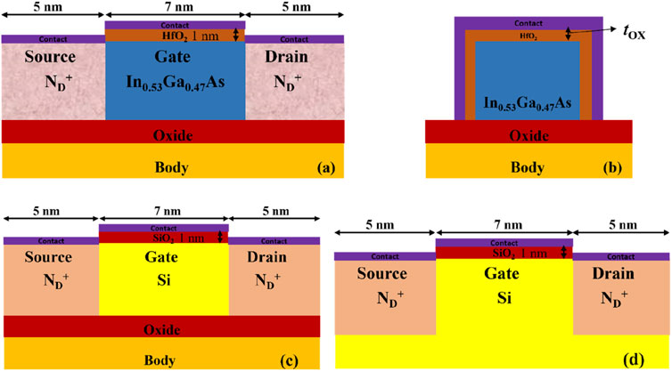
Figure 1. (A) InGaAs-SOI-FinFET (2D view), (B) InGaAs-SOI-FinFET (cross-sectional), (C) 2D side view of SOI-FinFET, (D) 2D side view of C-FinFET.
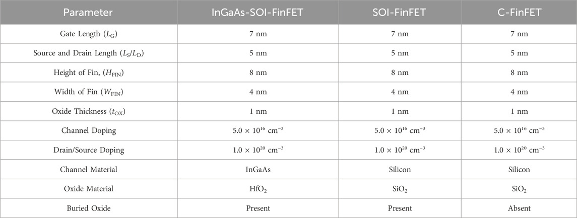
Table 1. Devices process parameters.
3 Methodology for simulation
The proposed InGaAs-SOI FinFET was simulated using the powerful 3D device simulator ATLAS (Silvaco, 2011). The models and features employed in the ATLAS simulation for the proposed device may vary depending on the specific requirements of the simulation and the technology node of the FinFET being modeled. Researchers and engineers often adjust simulation parameters to align with the characteristics of the devices they are studying. In this simulation, the Lombardi model, also known as the Constant Voltage and Temperature (CVT) mobility model, is applied to account for field-dependent mobility, as well as mobility degradation due to phonon and surface roughness scattering, and ionized impurity scattering. The Shockley-Read-Hall (SRH) model is utilized to analyze recombination effects by simulating leakage current caused by thermal factors. Additionally, the decoupling method, or Gummel’s method, is used for the Newton solution iteration (Silvaco, 2011). T = 300 K was the fixed device temperature for the duration of the simulation.
4 Experimental calibration and fabrication feasibility
To validate the simulation models used in this study, we calibrated them with experimental data from In0.53Ga0.47As -based FinFETs as reported in (Huang et al., 2015) and depicted in Figure 2. A FinFET with a gate length of 1 µm was created and simulated using a gate voltage of 0.75 V and a drain voltage of 0.5 V, mirroring the conditions of the experimental setup. The comparison of results confirms that our simulation models align well with the experimental data, demonstrating the validity of the models.
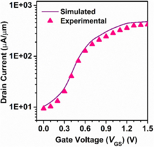
Figure 2. IDS vs. VGS plot for the calibration of used models with experimental work (Wu et al., 2023).
Moreover, Figure 3 shows the sequential procedure for determining the feasibility of the suggested device construction. The fabrication of InGaAs-SOI-FinFETs is a sophisticated process that integrates advanced materials and processes to leverage the superior electronic properties of InGaAs and the structural advantages of SOI and FinFET architectures. The following steps are involved in the fabrication process of the proposed device.
• First, the SOI wafers are cleaned, and then the fins are patterned using SAQP technique (Auth et al., 2017).
• Two self-aligned double patterns (SADP) are applied in a row and referred to as SAQP in order to improve the feature density.
• Next, orientation-dependent wet etching is employed to generate the Fin-channel (InGaAs), and an additional mask is used in this procedure.
• HfO2 is deposited by atomic layer deposition (ALD) on InGaAs interfacial layer (Choi et al., 2020).
• Next, metal gate deposition at room temperature is accomplished via electron beam evaporation.
• The final fabrication step includes contact etches and metal deposition. Therefore, the process flow of device design techniques can be used to fabricate InGaAs-SOI-FinFET.
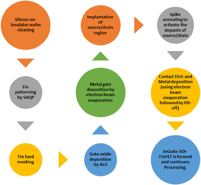
Figure 3. Fabrication flow chart of InGaAs-SOI-FinFET.
5 Results and discussion
The enhancement of drain current in InGaAs-SOI-FinFET is clearly observed (by ∼75% and ∼77%) as compared to SOI-FinFET and C-FinFET as shown in Figure 4A. InGaAs has significantly higher electron mobility compared to silicon (used in SOI-FinFET and C-FinFET). The higher mobility in InGaAs leads to faster carrier transport through the channel, which enhances the drain current. In contrast, silicon-based devices (SOI-FinFET and C-FinFET) exhibit lower mobility, limiting the current conduction. InGaAs have a lower electron-effective mass compared to silicon, which further contributes to higher velocity and better carrier transport, thereby increasing the drain current. InGaAs have a lower density of states than silicon, meaning fewer electrons are required to achieve a given carrier density. This enhances carrier injection into the channel, improving the overall current driving capability of the InGaAs-SOI-FinFET. The combination of high electron mobility and low effective mass in InGaAs leads to higher carrier velocity, which directly increases the drain current in InGaAs-SOI-FinFET at a given gate length. This is especially beneficial at 7 nm gate lengths, where short-channel effects become more prominent. Compared to SOI-FinFET and C-FinFET, the transconductance of the InGaAs-SOI-FinFET improves by approximately 46.15% and 53.84%, respectively, because of the InGaAs in the channel with high-k gate material and the drain current as shown in Figure 4B.
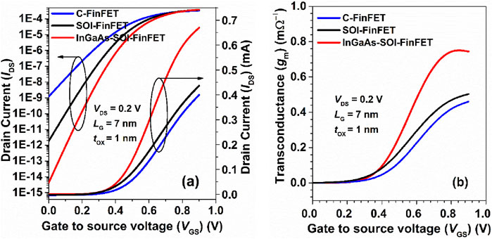
Figure 4. (A) IDS vs. VGS characteristics, and (B) Transconductance (gm); of C-FinFET, SOI-FinFET, and InGaAs-SOI-FinFET.
Drain current w.r.t. gate voltage (IDS vs. VGS) characteristics are shown in Figure 4A and for C-FinFET, SOI-FinFET, and InGaAs-SOI-FinFET. The figure shows that InGaAs-SOI-FinFET shows superior performance compared to conventional silicon FinFETs due to the superior electron mobility of InGaAs compared to silicon. This means that electrons can move more freely through the InGaAs channel, resulting in higher current flow for a given electric field. The higher electron mobility translates to higher drive currents and better device performance. InGaAs have a lower effective mass for electrons compared to silicon. This property allows electrons to accelerate more quickly under an electric field, resulting in higher current densities and, thus, enhanced drain current. InGaAs-SOI-FinFET can mitigate short channel effects (subthreshold swing degradation and such as drain-induced barrier lowering) better than silicon FinFETs due to the higher electron mobility and narrower bandgap. This allows for better control of the transistor behaviour at smaller device dimensions, leading to higher drain currents and improved performance. The combination of high electron mobility and bandgap engineering in InGaAs-SOI-FinFET enables better control over the transistor’s on/off current ratios. This is crucial for minimising leakage current in the off-state while maximizing current flow in the on-state, resulting in enhanced overall device performance.
The transconductance (gm) of InGaAs-SOI-FinFET is shown in Figure 4B and is simultaneously compared with SOI-FinFET and C-FinFET. Figure 4B shows that the combination of higher electron mobility, reduced channel length modulation, improved subthreshold swing, enhanced gate control, and optimized bandgap engineering in InGaAs-SOI-FinFET leads to an enhancement in drain transconductance compared to conventional FinFETs. These factors make InGaAs-SOI-FinFET promising candidates for high-performance electronic devices, particularly in applications where high-speed operation and low power consumption are crucial (Kumar et al., 2023). The energy band profile is displayed in terms of the valence band and conduction band in Figures 5A, B, respectively. It is concurrently compared with two other counterpart devices, SOI-FinFET and C-FinFET. InGaAs-SOI-FinFET has a better conduction band profile than SOI-FinFET and C-FinFET, as shown in Figure 5A. Likewise, Figure 5B demonstrates that InGaAs-SOI-FinFET has a better valence band profile than SOI-FinFET and C-FinFET. Because III-V compound semiconductors have tiny band gaps, the suggested device exhibits better energy bands, making it appropriate for high-performance analogue and low-power logic applications.
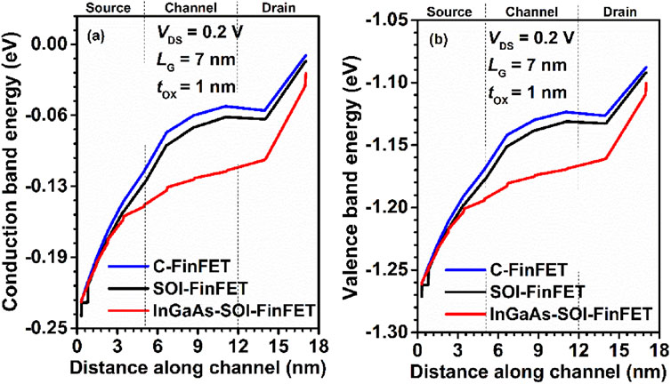
Figure 5. (A) Conduction band, and (B) Valence band profiles of InGaAs-SOI-FinFET, SOI-FinFET, and C-FinFET.
Improvements (reduction) in second-order (gm2) and third-order transconductance (gm3) in FinFETs are crucial for enhancing device performance, particularly in high-speed and high-frequency applications. Figures 6A, B reflect the gm2 and gm3, respectively, for InGaAs-SOI-FinFET, SOI-FinFET, and C-FinFET and calculated by using Equation 1; (Kumar and Chaujar, 2021a). Figures 6A, B show that these higher-order transconductances are improved due to better control over short-channel effects in the proposed structure compared to planar FETs. The three-dimensional fin structure helps to mitigate issues like drain-induced barrier lowering (DIBL) and subthreshold swing degradation, which can degrade transconductance in traditional FETs. InGaAs material and structure improve carrier mobility, and transport characteristics improve the higher-order transconductances. By using materials with higher electron mobility or implementing strain engineering techniques, it's possible to enhance transconductance. Advanced gate dielectric materials and processes can reduce gate leakage and improve gate capacitance. High-k (HfO2) dielectrics with low interface trap densities are commonly employed to achieve better gate control and, consequently, higher transconductance. Proper doping of the source, drain, and channel regions is crucial for achieving high transconductance. Optimizing the doping profile helps to minimize series resistance and improve carrier transport efficiency in InGaAs-SOI-FinFET as compared to its counterparts.
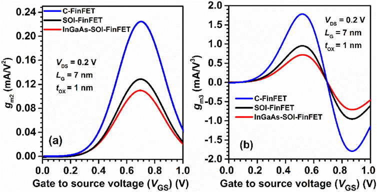
Figure 6. (A) gm2, and (B) gm3; of C-FinFET, SOI-FinFET, and InGaAs-SOI-FinFET.
Improvements in VIP2 (Second order voltage intercept point) and VIP3 (Third order voltage intercept point) in FinFETs are critical for enhancing the performance of RF, linearity and mmWave (millimeter-wave) applications for devices and circuits. Figures 7A, B show the VIP2 and VIP3 for InGaAs-SOI-FinFET and simultaneously compared with SOI-FinFET and C-FinFET. VIP2 and VIP3 are calculated by using Equations 2, 3; (Kumar and Chaujar, 2022). VIP2 and VIP3 are improved in InGaAs-SOI-FinFET due to advanced gate dielectric materials with high-k (HfO2) and low interface trap densities can improve gate control and reduce gate leakage, leading to better VIP2 and VIP3 figures of merit (Agrwal and Kumar, 2024). Choosing the appropriate semiconductor material for the FinFET channel, such as III-V compounds like InGaAs, in the proposed device significantly enhances carrier mobility and reduces noise, thereby improving VIP2 and VIP3.
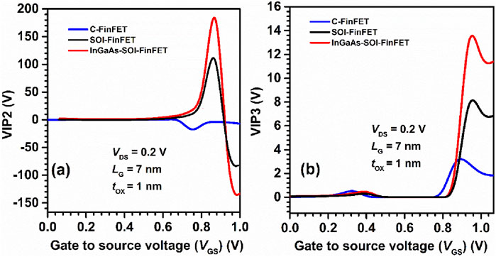
Figure 7. (A) VIP2, and (B) VIP3; of C-FinFET, SOI-FinFET, and InGaAs-SOI-FinFET.
IIP3 (Third Order Input Intercept Point) and IMD3 (Third Order Intermodulation Distortion) are evaluated using Equations 4, 5; (Kumar and Chaujar, 2022) and plotted w. r.t gate voltage for InGaAs-SOI-FinFET, SOI-FinFET, and C-FinFET as shown in Figure 8A, B respectively. IIP3 and IMD3 are the essential parameters for FinFET devices to enhance the linearity and performance of RF and mmWave (millimeter-wave) applications. IIP3 is a critical parameter in assessing the linearity of RF and analog circuits since third-order intermodulation products often fall within the operational frequency band, causing signal interference. Figure 8 shows that InGaAs-SOI-FinFET inherently exhibits better linearity compared to SOI-FinFET and C-FinFET due to reduced short-channel effects and improved gate control. This inherent linearity contributes to improved IIP3 and IMD3 performance. Choosing the appropriate semiconductor material for the channel, III-V compounds like InGaAs significantly enhance carrier mobility and reduce nonlinearity, thereby improving IIP3 and IMD3, as shown in Figure 8A, B, respectively. HfO2 improves gate control and reduces gate leakage, leading to better linearity and improved IIP3 and IMD3 figures. In the proposed device, only 0.2 V drain to source voltage (VDS) is applied which minimizing power supply noise and ensuring stable biasing conditions can help reduce nonlinear effects such as intermodulation distortion, improving IIP3 and IMD3 performance.
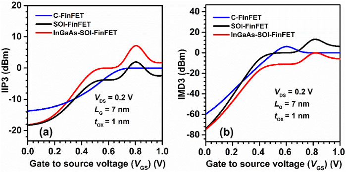
Figure 8. (A) IIP3, and (B) IMD3; of C-FinFET, SOI-FinFET, and InGaAs-SOI-FinFET.
The 1 dB Compression Point (P1dB) is a critical parameter in RF/microwave devices and analog circuits, including FinFETs, as it characterises the device’s linearity and power handling capability. P1dB is defined as the input power level at which the output power starts to deviate by 1 dB from the linear response. In order to enhance the linearity performance and reduce the distortion, P1dB is calculated using Equation 6; (Kumar and Chaujar, 2022) and plotted w.r.t. gate voltage for InGaAs-SOI-FinFET, SOI-FinFET, and C-FinFET with constant VDS of 0.2 V as shown in Figure 9. In InGaAs-SOI-FinFET the channel is created with material InGaAs which significantly enhance carrier mobility and reduce nonlinearity, thereby improving P1dB as shown in Figure 9. HfO2 improves gate control and reduce gate leakage, leading to better linearity and improved P1dB. From Equation 6, the reduction of higher order transconductance (shown in Figure 6B) and enhanced gm1 (shown in Figure 4B) leads to enhance the P1dB in InGaAs-SOI-FinFET as compared to SOI-FinFET, and C-FinFET as shown in Figure 9.
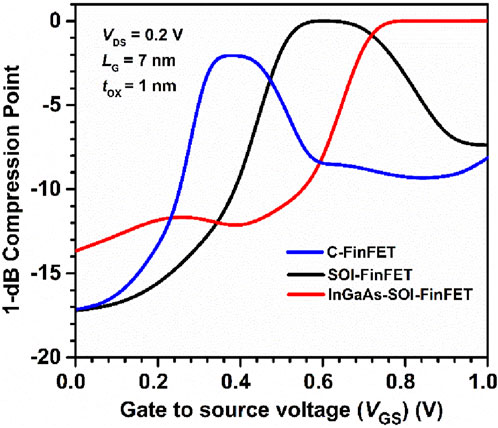
Figure 9. 1-dB compression point of C-FinFET, SOI-FinFET, and InGaAs-SOI-FinFET.
Further, to evaluate the distortion, HD2 (Second Harmonic Distortion) and HD3 (Third Harmonic Distortion) are calculated using Equations 7, 8; (Kumar and Chaujar, 2022; Kumar et al., 2018; Kumar and Chaujar, 2021b; Gupta and Kumar, 2020; Gupta and Kumar, 2021; Gupta and Kumar, 2022) w.r.t. gate bias for C-FinFET, SOI-FinFET, and InGaAs-SOI-FinFET as shown in Figures 10A, 8B respectively. HD2 and HD3 are important parameters in FinFETs for enhancing the linearity and signal fidelity in RF and microwave applications. InGaAs-SOI-FinFET inherently exhibits reduced short-channel effects compared to traditional planar FETs, leading to improved linearity and lower harmonic distortion. Choosing semiconductor materials with high carrier mobility and low nonlinearity, such as InGaAs, reduces distortion and improves linearity in InGaAs-SOI-FinFET. High HD2 can distort signals in RF circuits, especially where linearity is critical. HD3 is often more problematic than HD2 in practical RF circuits, as it can fall within the band of interest, causing intermodulation and distortion directly on useful signal components. Better linearity and lower harmonic distortion are also observed in InGaAs-SOI-FinFET owing to HfO2 as a gate dielectric material. Scaling down the gate length (7 nm) in the proposed device improves gate control and reduces parasitic capacitances, leading to higher linearity and lower harmonic distortion. From Equations 7, 8, the enhanced gm1 (shown in Figure 4B) leads to reduce the HD2 and HD3 in InGaAs-SOI-FinFET as compared to SOI-FinFET and C-FinFET as shown in Figures 10A, B respectively.
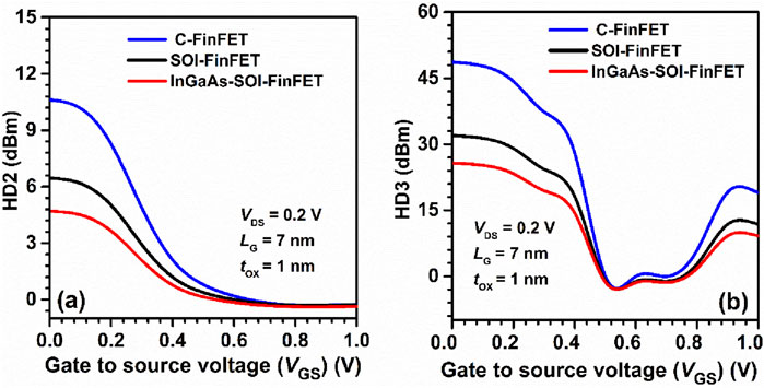
Figure 10. (A) HD2, and (B) HD3; of C-FinFET, SOI-FinFET, and InGaAs-SOI-FinFET.
Further, the device parasitic capacitances such as gate-to-source (CGS), gate-to-drain (CGD), and gate-to-gate (CGG) capacitances are shown in Figures 11A–C respectively. From the figure, it is evident that the parasitic capacitances are significantly reduced in C-FinFET, SOI-FinFET, and InGaAs-SOI-FinFET. Improving parasitic capacitances in InGaAs-SOI-FinFET is crucial for achieving higher device performance, especially in terms of speed, power efficiency, and signal integrity. InGaAs-SOI-FinFET is inherently designed with a three-dimensional fin structure, which reduces parasitic capacitances compared to traditional planar FETs. FinFETs typically have lower junction capacitances due to the reduced area of the source and drain regions, leading to lower parasitic capacitances. HfO2, as a high-k dielectric material with higher permittivity, is often used to replace traditional silicon dioxide (SiO2) to achieve better gate control and lower parasitic capacitances. InGaAs-SOI-FinFET is scaled down to 7 nm, which helps reduce gate-to-channel capacitance and leads to improved performance. However, this scaling needs to be balanced with challenges such as short-channel effects and increased leakage currents. Employing advanced isolation techniques such as silicon-on-insulator (SOI) technology also helps reduce parasitic capacitances and improve device performance, as shown in Figure 11.
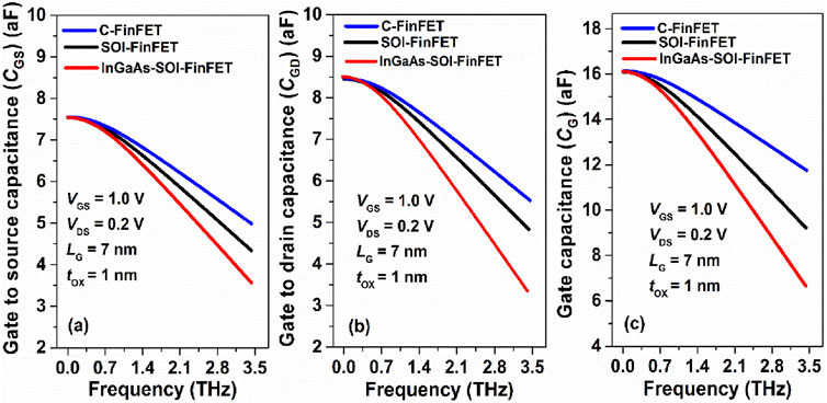
Figure 11. (A) Cgs, (B) Cgd, and (C) CGG; of C-FinFET, SOI-FinFET, and InGaAs-SOI-FinFET.
The transition frequency (fT) and maximum oscillation frequency (fMAX) are essential parameters in FinFETs, particularly for RF applications, as they directly influence the device’s performance at high frequencies. fT and fMAX represent the frequency at which the transistor’s current gain and power gain start to roll off, respectively. In RF applications, where high-frequency signals are common, it's crucial to have transistors with high fT and fMAX to maintain signal integrity and fidelity. fT and fMAX are evaluated using Equations 9, 10, respectively, for InGaAs-SOI-FinFET, SOI-FinFET, and C-FinFET as shown in Figures 12A, B. From Figures 12A, B, it is also observed that fT and fMAX are improved in InGaAs-SOI-FinFET as compared to SOI-FinFET and C-FinFET. The higher value of fT and fMAX in the InGaAs-SOI-FinFET device is indicative of the transistor’s ability to provide linear amplification and high gain at RF frequencies. This is essential for maintaining signal quality and avoiding distortion in RF systems. With the higher value of fT and fMAX, InGaAs-SOI-FinFET can operate effectively at higher frequencies without significant degradation in performance. This is critical for RF applications requiring wide bandwidth and fast signal processing. It can also achieve higher power efficiency at RF frequencies since it can operate closer to its maximum frequency capabilities, leading to reduced power consumption for the same output power. Therefore, RF systems’ performance heavily relies on individual transistors’ characteristics. InGaAs-SOI-FinFET with high fT and fMAX contribute to the overall system performance by enabling higher-speed signal processing, wider frequency coverage, and improved signal quality.
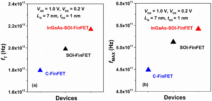
Figure 12. (A) fT, and (B) fMAX; of C-FinFET, SOI-FinFET, and InGaAs-SOI-FinFET.
In RF applications, especially those requiring high-performance transistors like FinFETs, several key parameters are essential for determining the device’s suitability and performance. GFP (Gate to Source/Drain Forward Transconductance), TFP (Transconductance Frequency Product), and GTFP (Gate to Source/Drain Transconductance Frequency Product) are among these crucial parameters and calculated by using Equations 11–13 respectively (Kumar and Chaujar, 2021a; Kumar and Chaujar, 2022). GFP represents the rate of change of the output current with respect to the input voltage, indicating how effectively the transistor can amplify input signals. In RF applications, high GFP is essential for achieving high gain and signal amplification, as it directly influences the transconductance of the device. Figure 13A shows the higher GFP in InGaAs-SOI-FinFET as compared to SOI-FinFET and C-FinFET. Higher GFP provides better linearity, higher gain, and improved signal-to-noise ratio in RF amplifiers and other RF circuits. TFP is the product of transconductance and frequency, representing the rate of change of output current with respect to the input voltage and frequency, and it is shown in Figure 13B for InGaAs-SOI-FinFET, SOI-FinFET, and C-FinFET. Higher TFP in InGaAs-SOI-FinFET indicates that the device can maintain its transconductance over a wider range of frequencies, which is critical for RF applications where signals span a broad frequency spectrum. InGaAs-SOI-FinFET with higher TFP provides consistent performance across a range of frequencies, enabling them to be used in broadband RF circuits with minimal distortion. GTFP is also evaluated using Equation 13 for all three devices, as shown in Figure 13B. GTFP combines the effects of GFP and TFP, providing a comprehensive measure of the device’s performance in RF applications. High GTFP in InGaAs-SOI-FinFET indicates that the device can provide both high transconductance and maintain it over a wide frequency range, making it suitable for RF amplification and signal processing. InGaAs-SOI-FinFET with high GTFP is desirable for RF applications where both gain and bandwidth are crucial, such as in wireless communication systems, radar, and satellite communication. Thus, InGaAs-SOI-FinFET is more suitable for RF applications as the higher GFP, TFP, and GTFP are essential for designing RF circuits and systems.
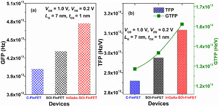
Figure 13. (A) Gfp, and (B) TFP, GTFP; of C-FinFET, SOI-FinFET, and InGaAs-SOI-FinFET.
Therefore, the proposed device shows excellent performance as compared to its conventional counterparts, as shown in Table 2. Table 2 shows the results comparison of InGaAs-SOI-FinFET with C-FinFET and SOI-FinFET and indicates that the proposed device is more suitable for RF applications, designing RF circuits and systems that meet the stringent requirements of modern wireless communication standards and applications.
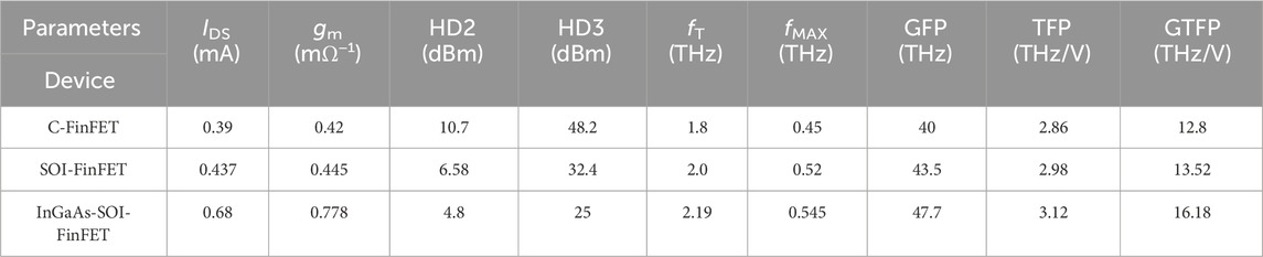
Table 2. Results comparison.
6 Conclusion
In conclusion, the advancements in InGaAs-SOI-FinFET technology with improved RF and linearity parameters represent a significant leap forward in the field of RF electronics. In0.53Ga0.47As SOI-FinFET has emerged as a promising candidate for next-generation RF applications through meticulous material engineering and innovative device designs. The incorporation of InGaAs as the channel material brings forth its superior electron mobility and excellent high-frequency characteristics, making it well-suited for RF circuits demanding high-speed signal processing and wide bandwidths. Moreover, the unique three-dimensional fin structure of FinFETs mitigates short-channel effects and enhances gate control, resulting in improved linearity and reduced distortion at high frequencies. Key parameters such as fT, fMAX, TFP, GFP, and GTFP have significantly enhanced amplification capabilities, broader bandwidths, and consistent performance across frequency ranges. These improvements pave the way for the development of highly efficient and reliable RF systems, enabling applications ranging from wireless communications and radar to satellite communication and beyond.
Data availability statement
The original contributions presented in the study are included in the article/supplementary material, further inquiries can be directed to the corresponding author.
Author contributions
PA: Conceptualization, Investigation, Writing–original draft, Writing–review and editing. AK: Investigation, Resources, Software, Supervision, Writing–original draft, Writing–review and editing.
Funding
The author(s) declare that no financial support was received for the research, authorship, and/or publication of this article.
Conflict of interest
The authors declare that the research was conducted in the absence of any commercial or financial relationships that could be construed as a potential conflict of interest.
Publisher’s note
All claims expressed in this article are solely those of the authors and do not necessarily represent those of their affiliated organizations, or those of the publisher, the editors and the reviewers. Any product that may be evaluated in this article, or claim that may be made by its manufacturer, is not guaranteed or endorsed by the publisher.
References
Agrwal, P., and Kumar, A. (2024). Reliability investigation of interfacial defects in InGaAs-SOI-FinFET for high-performance applications. Indian J. Pure Appl. Phys. 62 (11), 1004–1011. doi:10.56042/ijpap.v62i11.12442
Ajayan, J., and Nirmal, D. (2015). A review of InP/InAlAs/InGaAs based transistors for high frequency applications. Superlattices Microstruct. 86, 1–19. doi:10.1016/j.spmi.2015.06.048
Auth, C., Aliyarukunju, A., Asoro, M., Bergstrom, D., Bhagwat, V., Birdsall, V., et al. (2017). “A 10nm high performance and low-power CMOS technology featuring 3 rd generation FinFET transistors, Self-Aligned Quad Patterning, contact over active gate and cobalt local interconnects,” in 2017 IEEE international electron devices meeting (IEDM) (IEEE), 29.1. 1–29.1. 4.
Boukortt, N., Hadri, B., and Caddemi, A. (2016). Simulation of a nanoscale SOI TG nFinFET. Int. J. Comput. Appl. 138, 10–14. doi:10.5120/ijca2016908981
Boukortt, N., Hadri, B., Patanè, S., Caddemi, A., and Crupi, G. (2017). Investigation on TG n-FinFET parameters by varying channel doping concentration and gate length. Silicon 9 (6), 885–893. doi:10.1007/s12633-016-9528-3
Bousari, N. B., Anvarifard, M. K., and Haji-Nasiri, S. (2019). Improving the electrical characteristics of nanoscale triple-gate junctionless FinFET using gate oxide engineering. AEU-International J. Electron. Commun. 108, 226–234. doi:10.1016/j.aeue.2019.06.017
Choi, S.-N., Moon, S.-E., and Yoon, S.-M. (2020). Impact of oxide gate electrode for ferroelectric field-effect transistors with metal-ferroelectric-metal-insulator-semiconductor gate stack using undoped HfO2 thin films prepared by atomic layer deposition. Nanotechnology 32 (8), 085709. doi:10.1088/1361-6528/abc98c
Del Alamo, J. A. (2011). Nanometre-scale electronics with III–V compound semiconductors. Nature 479 (7373), 317–323. doi:10.1038/nature10677
Fletcher, A. A., Nirmal, D., Ajayan, J., and Arivazhagan, L. (2019). Analysis of AlGaN/GaN HEMT using discrete field plate technique for high power and high frequency applications. AEU-International J. Electron. Commun. 99, 325–330. doi:10.1016/j.aeue.2018.12.006
Gupta, A., Mathur, R., and Nizamuddin, M. (2019). Design, simulation and comparative analysis of a novel FinFET based astable multivibrator. AEU-International J. Electron. Commun. 100, 163–171. doi:10.1016/j.aeue.2018.12.007
Gupta, N., and Kumar, A. (2020). Assessment of high-k gate stack on sub-10nm SOI-FinFET for high-performance analog and RF applications perspective. ECS J. Solid State Sci. Technol. 9 (12), 123009. doi:10.1149/2162-8777/abcf14
Gupta, N., and Kumar, A. (2021). Numerical assessment of high-k spacer on symmetric S/D underlap GAA junctionless accumulation mode silicon nanowire MOSFET for RFIC design. Appl. Phys. A 127 (1), 76–78. doi:10.1007/s00339-020-04234-6
Gupta, N., and Kumar, A. (2022). Influence of GaN/ZrO2 interfacial layer defects on 8-nm GaN-SOI-FinFET for reliable RFIC design. AEU-International J. Electron. Commun. 144, 154045. doi:10.1016/j.aeue.2021.154045
Huang, M., Chang, S. W., Chem, M. K., Fan, C. H., Lin, C. H., Lin, H. T., et al. (2015). “0.53 Ga 0.47 as MOSFETs with high channel mobility and gate stack quality fabricated on 300 mm Si substrate,” in 2015 symposium on VLSI technology (VLSI technology) (IEEE), T204–T205.
Jiang, Z., Behin-Aein, B., Krivokapic, Z., Povolotskyi, M., and Klimeck, G. (2015). Tunneling and short channel effects in ultrascaled InGaAs double gate MOSFETs. IEEE Trans. Electron Devices 62 (2), 525–531. doi:10.1109/ted.2014.2383392
Kim, S.-D., Guillorn, M., Lauer, I., Oldiges, P., Hook, T., and Na, M.-H. (2015). “Performance trade-offs in FinFET and gate-all-around device architectures for 7nm-node and beyond,” in 2015 IEEE SOI-3D-Subthreshold microelectronics technology unified conference (S3S) (IEEE), 1–3.
Ko, H. L., Luc, Q. H., Huang, P., Chen, S. M., Wu, J. Y., Hsu, C. W., et al. (2021). Nitrogen-pPassivated (010) In0.53Ga0.47As FinFETs With High Peak gm and Reduced Leakage Current. IEEE Trans.actions on Electron Devices 69 (2), 495–499. doi:10.1109/ted.2021.3133222
Ko, H.-L., Luc, Q. H., Huang, P., Chen, S. M., Wu, J. Y., Tran, N. A., et al. (2022). Electrical characteristics of in 0.53 Ga 0.47 as gate-all-around MOSFETs with different nanowire shapes. IEEE Trans. Electron Devices 69 (8), 4183–4187. doi:10.1109/ted.2022.3181572
Kumar, A., Chhabra, A., and Chaujar, R. (2018). GaAs junctionless FinFET using high-k dielectric for high-performance applications. Kyiv, UKraine, 24-26 April 2018 (IEEE) 126–129.
Kumar, B., and Chaujar, R. (2021a). Analog and RF performance evaluation of junctionless accumulation mode (JAM) gate stack gate all around (GS-GAA) FinFET. Silicon 13, 919–927. doi:10.1007/s12633-020-00910-7
Kumar, B., and Chaujar, R. (2021b). Analog and RF performance evaluation of junctionless accumulation mode (JAM) gate stack gate all around (GS-GAA) FinFET. Silicon 13 (3), 919–927. doi:10.1007/s12633-020-00910-7
Kumar, B., and Chaujar, R. (2022). Numerical study of JAM-GS-GAA FinFET: a Fin aspect ratio optimization for upgraded analog and intermodulation distortion performance. Silicon 14 (1), 309–321. doi:10.1007/s12633-021-01395-8
Kumar, B., Sharma, M., and Chaujar, R. (2023). Gate electrode work function engineered JAM-GS-GAA FinFET for analog/RF applications: performance estimation and optimization. Microelectron. J. 135, 105766. doi:10.1016/j.mejo.2023.105766
Minaei, S., and Yuce, E. (2012). A simple CMOS-based inductor simulator and frequency performance improvement techniques. AEU-International J. Electron. Commun. 66 (11), 884–891. doi:10.1016/j.aeue.2012.03.005
Poljak, M., Jovanović, V., and Suligoj, T. (2009). Improving bulk FinFET DC performance in comparison to SOI FinFET. Microelectron. Eng. 86 (10), 2078–2085. doi:10.1016/j.mee.2009.01.066
Sonnet, A., Hinkle, C. L., Jivani, M. N., Chapman, R. A., Pollack, G. P., Wallace, R. M., et al. (2008). Performance enhancement of n-channel inversion type InxGa1− xAs metal-oxide-semiconductor field effect transistor using ex situ deposited thin amorphous silicon layer. Appl. Phys. Lett. 93 (12). doi:10.1063/1.2991340
Takahashi, T., Kawano, Y., Makiyama, K., Shiba, S., Sato, M., Nakasha, Y., et al. (2016). Enhancement of fmax to 910 GHz by adopting asymmetric gate recess and double-side-doped structure in 75-nm-Gate InAlAs/InGaAs HEMTs. IEEE Trans. Electron Devices 64 (1), 89–95. doi:10.1109/ted.2016.2624899
Wu, J.-Y., Huang, P., Luc, Q. H., Ko, H. L., Chiang, Y. C., Yu, H. C., et al. (2023). High performance inversion-mode in 0.53 Ga 0.47 as FinFETs for logic and RF applications. IEEE Trans. Nanotechnol. 22, 445–448. doi:10.1109/tnano.2023.3303832
Xue, F., Jiang, A., Chen, Y. T., Wang, Y., Zhou, F., Chang, Y. F., et al. (2014). Nonplanar InGaAs gate wrapped around field-effect transistors. IEEE Trans. Electron Devices 61 (7), 2332–2337. doi:10.1109/ted.2014.2320946
Zota, C. B., Lindelow, F., Wernersson, L., and Lind, E. (2016a). “InGaAs nanowire MOSFETs with Ion= 555 µA/µm at Ioff= 100 nA/µm and VDD= 0.5 V,” in 2016 IEEE Symposium on VLSI Technology (Honolulu, HI: IEEE).
Zota, C. B., Lindelow, F., Wernersson, L.-E., and Lind, E. (2016b). “InGaAs tri-gate MOSFETs with record on-current,” in 2016 IEEE international electron devices meeting (IEDM) (IEEE), 3.2. 1–3.2. 4.
Keywords: C-FinFET, InGaAs-SOI-FinFET, linearity, SOI-FinFET, RF
Citation: Agrwal P and Kumar A (2025) Comprehensive analysis of In0.53Ga0.47As SOI-FinFET for enhanced RF/wireless performance. Front. Electron. 6:1497940. doi: 10.3389/felec.2025.1497940
Received: 18 September 2024; Accepted: 13 January 2025;
Published: 03 February 2025.
Edited by:
Sungsik Lee, Pusan National University, Republic of KoreaReviewed by:
Naushad Alam, Aligarh Muslim University, IndiaNaveen Kumar, University of Glasgow, United Kingdom
Copyright © 2025 Agrwal and Kumar. This is an open-access article distributed under the terms of the Creative Commons Attribution License (CC BY). The use, distribution or reproduction in other forums is permitted, provided the original author(s) and the copyright owner(s) are credited and that the original publication in this journal is cited, in accordance with accepted academic practice. No use, distribution or reproduction is permitted which does not comply with these terms.
*Correspondence: Ajay Kumar, YWpheS5rdW1hckBqaWl0LmFjLmlu