 Hae-in Kim
 Alexander Wilcher
 Yong-Kyu Yoon
95% of researchers rate our articles as excellent or good
Learn more about the work of our research integrity team to safeguard the quality of each article we publish.
Find out more
BRIEF RESEARCH REPORT article
Front. Electron. , 14 February 2025
Sec. Nano- and Microelectronics
Volume 6 - 2025 | https://doi.org/10.3389/felec.2025.1493911
This paper presents an innovative interconnect approach called “meta-interconnect,” which utilizes a combination of copper (Cu) and cobalt (Co) metaconductor (Cu/Co-MC) to enhance signal integrity in the millimeter-wave (mm-wave) spectrum. The primary objective is to demonstrate reduced conductor losses from the skin effect compared to Cu at the 112 Gbps Nyquist frequency of 28 GHz. For the first time, a comprehensive parametric analysis is conducted using both simulation and experimentation methods to suppress the skin effect with Cu/Co-MC. Based on the optimization of Cu/Co-MC-based coplanar waveguide (CPW) transmission lines, a minimum insertion loss of only 0.08 dB/mm at 28 GHz, which is 0.06 dB/mm less than that of the Cu counterpart, has been demonstrated, which represents a 42.86% reduction in conductor power losses. Additionally, Cu/Co-MC-based CPWs meet the sub-0.1 dB/mm channel loss target. The study verifies the impact that the thickness and number of Cu/Co-MC layers have on device performances. This provides valuable insights into the optimizing MC configurations, which in this study are 250 nm thick Cu and 40 nm thick Co. Cu/Co-MC pairs with optimized layers and total thicknesses demonstrate significant improvements in insertion loss and thermal noise. These findings highlight the potential benefits of the Cu/Co-MC-based meta-interconnect technology for data center high-speed serial bus applications, offering a promising solution for achieving high signal integrity in the mm-wave spectrum, contributing to the overall understanding and its MCs translation to commercial applications.
The deployment of the millimeter wave (mm-wave) spectrum has led to various applications such as the Internet of Things (IoT), 5G mobile communication (Qualcomm, 2018; Rappaport et al., 2017), vehicle-to-everything (V2X) (Prathiba et al., 2021; He et al., 2020), and edge/cloud computing (Nouri et al., 2020), to name a few. Among them, high-bandwidth data center networking is one of the most preeminent applications for the explosive growth in network data traffic (Razdan et al., 2022; Kim et al., 2019). To enable future 800 Gigabit Ethernet (800 GE) applications, the development of a highly energy-efficient serial/de-serial (SerDes) transceiver with a data rate above 100 Gbps is imperative, which entails more stringent receiver specifications, such as reduced channel budgets from high electrical loss (Kim et al., 2019; Salem et al., 2020; Kim H.-I. et al., 2022). This necessitates a low-loss interconnect at a Nyquist frequency greater than 26.5 GHz, through which an advanced network interface improves the signal integrity of the high-speed transceiver. As shown in Figure 1, the length requirement for 112 Gbps common electrical I/O (CEI) can vary from 5 cm to 1 m per lane (Anon, 2023). In the context of 800 GE applications involving eight lanes of 112 Gbps serial bus, the utilization of a low-loss interconnect can significantly enhance the performance of the SerDes transceiver. Various advanced packaging configurations have been proposed in recent years, including co-packaged optical interconnects (Razdan et al., 2022; Testa et al., 2022), and wireless interconnects (Kim Y. et al., 2022; Hwangbo et al., 2019). However, meeting the insertion loss requirement at 28 GHz remains challenging (Neves et al., 2016). The target of reducing loss to below 0.1 dB/mm is based on the IEEE 802.3 standard for Ethernet, which specifies that the differential mode insertion loss over a 2-m cable must not exceed 19.75 dB. This requirement translates to an approximate loss of 0.01 dB/mm. To address this issue, metaconductors consisting of non-magnetic (e.g., Cu, Al, and Au) and ferromagnetic multilayers (e.g., Ni, Co, and Fe) metals have been employed to minimize the skin effect inside conductors at various frequencies (Bowrothu et al., 2022; Kim et al., 2023). Previous studies have demonstrated the reduction of conductor loss by 32% at 51 GHz using Cu/Fe-MC for V-band (40–75 GHz) (Bowrothu and Yoon, 2020), as well as improved insertion loss in the interconnect at 28 GHz by employing Cu/Co-MC, which reduces electrical resistance by 50% (Hwangbo et al., 2018). For this study Co/Co-MC provides the ideal frequency range between ferromagnetic (FMR) and antiferromagnetic (AFMR) resonances, enabling a superlattice conductor with improved performance at the targeted operating frequency of 28 GHz. Other ferromagnetic materials, such as Ni (Clingenpeel and Yoon, 2017) have an AFMR below the operating frequency, whereas others, such as Fe, have been demonstrated to be promising candidates for performance enhancements at frequencies higher than the targeted frequency in this work (Bowrothu and Yoon, 2020). Nevertheless, these studies have limitations, including insertion losses exceeding 0.1 dB/mm, suboptimal metal thickness configurations, and discrepancies between simulation and measurement results due to architectural differences between microstrip lines and CPWs.
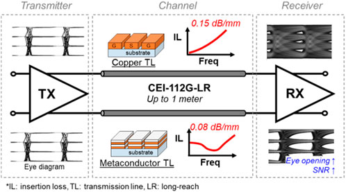
Figure 1. Schematic of the interconnects with 112 Gbps PAM-4 modulation. The metaconductor-based interconnect features low insertion loss at Nyquist frequency, resulting in a larger eye opening and a higher signal-to-noise ratio (SNR) than the Cu counterpart.
Here, we study the metaconductor-based interconnect, the so-called meta-interconnect based on Cu/Co-MC. The objective of this study is to optimize the Cu/Co-MC configuration to achieve an interconnect with an insertion loss of below 0.1 dB/mm toward a data rate of 112 Gbps at 28 GHz. Through a comprehensive parametric analysis utilizing CPW design and prototypes, the reduction of conductor loss will be validated by correlating the measurements from over 200 prototypes. In this work, CPW transmission lines and fabrication methods are chosen over striplines and alternatives due to practical considerations, including complexity, cost, and time. Notably, the impact of the number of Cu/Co-MC layers will be investigated for the first time, offering valuable insights into the optimal configuration of the Cu/Co-MC, and enhancing interconnect performance for 112 Gbps applications.
Metaconductors are superlattices composed of thin, alternating layers of standard conducting metals and ferromagnetic layers. The superlattice architecture is chosen over alloys or alternative configurations as it allows for the precise control of the material properties needed for designing low-loss RF conductors. The control and repeatability of fabrication techniques ensure that the magnetic properties of the ferromagnetic thin films are consistent when characterized.
For the ferromagnetic thin films used in this work the modification of the magnetic properties of the film due to the copper diamagnetic layers are considered negligible due to the thickness of the individual layers. As a result, the ferromagnetic films are assumed to retain their intrinsic magnetic properties when integrated into the superlattice structure.
Procedures such as those described by Hwangbo et al. (2018) and Bowrothu et al. (2022) can be used to approximate the effective permeability of the superlattice but rely on the material averaging concept enabled by the superlattice architecture. The application of the material averaging concept is difficult to achieve with the use of alternative architectures and as will be discussed later, clearly defined material interfaces/boundaries are required. Cu/Co metaconductors take this into consideration, as these interfaces/boundaries must not only start clearly defined but must remain stable throughout device lifetimes. The Co layers play an important role in maintaining these clear interfaces/boundaries by preventing the intermixing and diffusion of Cu into adjacent Co layers at moderate temperatures or temperatures less than 400C°. Moreover, this property of Co to inhibit Cu diffusion is a focus of active research in the semiconductor industry, as Co has been and continues to be explored as an interconnect liner/barrier to prevent the electromigration of Cu in interconnects, which leads to device failures, such as shorts between closely spaced interconnects.
If the thickness of each of these clearly defined layers is much less than both the skin depth and one-tenth of the wavelength of the operating frequency (λ/10), the individual layers are “perceived” by an electromagnetic wave as a bulk material with averaged properties. This allows for the engineering of material properties not readily found in nature. In the case of metaconductors, the aim is to engineer the effective permeability as close to zero as possible, which increases the skin depth, thereby increasing the cross-sectional area through which current flows, reducing resistive losses.
The initial basis for material averaging assumes that the layer materials are linear, homogeneous, isotropic, and exhibit negligible surface currents. For a transverse electromagnetic wave with wave vector (k), where the electric field is normal to the interface/boundary and the magnetic field (Ht) propagates parallel to the interface, magnetic boundary conditions dictate that the transverse magnetic field must be continuous across the boundary. Using these, the effective permeability of the superlattice may be approximated as follows.
The magnetic flux (Φi) through a cross-sectional area (Ai) is related to the material’s magnetic field and the material’s permeability, where area is defined by a width (w) and thickness (ti). The total magnetic flux is the sum of fluxes through the individual layers. By simplifying and rearranging terms, an effective permeability may be derived. Using ferromagnetic films with a well-defined magnetic property including a ferromagnetic resonance and range of negative permeability the effective permeability may be engineered to have a value near zero at a frequency of interest by controlling the thickness. Thus, as stated above the cross-sectional area may be increased and I2R losses minimized.
Cu/Co-MC-based transmission lines were designed using High Frequency Structure Simulator (HFSS, ANSYS Inc.). Low-loss SG3 glass (Corning Inc.) was used as a substrate, with a dielectric constant of 5.3 and a loss tangent of 0.004. Though the dielectric constant and loss tangent are frequency-dependent, the substrate used in this work each varies less than ±0.1 and ±0.002, respectively. These variations were deemed negligible for our modeling. CPW transmission lines were designed, and parametric studies were conducted to investigate:
1. The effects of individual layer thicknesses of Cu (tCu) and Co (tCo) in a Cu/Co-MC with a fixed ratio (R = tCu/tCo) of 6 and total thickness (ttotal) of 2 µm.
2. The effect of the ttotal of the Cu/Co-MC with the optimized individual layer thicknesses of tCu = 240 nm and tCo = 40 nm found by the first study.
In both parametric studies, the number of Cu/Co layers (N) varies either as a function of individual layer thicknesses tCu and tCo or as a function of ttotal.
The metal layer thickness of the Cu/Co-MC plays a crucial role in reducing conductor loss. In this analysis, we examined the impact of the different individual layer thicknesses of the Cu/Co-MC while keeping the ttotal fixed at 2 μm and the Cu/Co-MC R at 6. The specific cases studied have N = 2, 3, 6, 10, and 20. For each case, the film thickness of the Cu/Co-MC was as follows: 750 nm/125 nm for N = 2, 500 nm/80 nm for N = 3, 250 nm/40 nm for N = 6, 150 nm/25 nm for N = 10, and 75 nm/12.5 nm for N = 20. Figure 2A presents simulation results, assuming no interfacial roughness, which may be reasonable based on the later fabrication results and a magnetic material that is single-crystalline and uniformly magnetized to saturation. Within the frequency range of 5–45 GHz, we observed that reducing the thickness of each tCu and tCo layer and therefore increasing the total number of layers N leads to a greater reduction in insertion loss. For instance, the solid Cu-based design exhibited an insertion loss of 0.09 dB/mm at 28 GHz, whereas the Cu/Co-MC configurations with N = 2, 3, 6, 10, and 20 layers showed insertion losses of 0.058, 0.056, 0.055, 0.054, and 0.051 dB/mm, respectively. In the numerical analysis, the N = 20 configuration demonstrated the lowest insertion loss. This is attributed to the individual metal layers being much less than the skin depth at the center frequency (e.g., the skin depth of Cu at 28 GHz is 390 nm), making the bulk material effectively “appear” homogeneous to the electromagnetic wave, effectively canceling the eddy current produced from the time-varying magnetic field induced by the applied AC current. Skin depth results in an electromagnetic wave exponentially attenuating away from the surface toward the interior of a conductor. As a result, the Cu/Co-MC, with the thinnest metal layers, experiences minimal conductor losses. On the other hand, if each metal thickness becomes a significant fraction of the skin depth at the center frequency, the electromagnetic field “perceives” an inhomogeneous material and becomes confined to the individual metal layers, leading to increased electrical losses due to eddy current circulation.
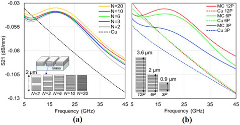
Figure 2. Simulation results of Cu/Co-MC. (A) Individual metal thickness variation with the thickness ratio between Cu and Co, R = 6, and (B) variation of the number of pairs with each pair of 250 nm-thick Cu and 40 nm-thick Co. Cu-based devices have an equivalent thickness to the total thickness of the metaconductor.
In the meantime, it is important to note that in physical manufacturing processes, a larger number of layers may result in performance degradation due to fabrication imperfections (e.g., surface roughness), non-ideal shape anisotropy of magnetic materials, and interface tolerances. Also, the increased number of layers may increase manufacturing costs as they must change the deposition step multiple times. Determining the optimal layer thicknesses would be contingent on the specific fabrication method used.
Evaluating the impact of ttotal on the performance of Cu/Co-MCs is important to the overall analysis of this study. A CPW unit cell was designed for this purpose, with the individual thickness of the Cu/Co-MC layers fixed at tCu = 240 nm and tCo = 40 nm with an R of 6. Three different ttotal of the Cu/Co-MC were investigated: a) 0.875 μm (N = 3), b) 1.75 μm (N = 6 pairs), and c) 5.25 μm (N = 12). The width of each transmission line was constant, and the reflections caused by impedance mismatches were removed by renormalizing the scattering parameters to match the impedance of each individual line. The simulation results were compared with Cu-based CPWs having an equivalent total ttotal to that of the Cu/Co-MCs. As depicted in Figure 2B, an increase in ttotal results in a decrease in resistance at the mm-wave frequency. The Cu-based designs with a ttotal equivalent to the N = 3, 6, and 12 Cu/Co-MC designs exhibited insertion losses of 0.98, 0.090, and 0.089 dB/mm at 28 GHz. In contrast, the Cu/Co-MC designs with a ttotal for N = 3, 6, and 12 Cu/Co-MC designs displayed resistance values of 0.073, 0.057, and 0.052 dB/mm at 28 GHz, respectively.
To validate the simulation results, CPW transmission lines were fabricated on a 300 μm thick SG3 glass wafer with sub-nanometer surface roughness. Metallization is achieved using a Kurt J. Lesker CMS-18 Magnetron Sputtering System to deposit Cu/Co-MC via RF and DC magnetron sputtering. While sputtering is employed to fabricate the metaconductor in this work, for CEI-112G-LR applications that support interconnect lengths between 1 and 2 m and broader commercial adoption, other methods are envisioned. Specifically, to address scaling and cost requirements, the electrodeposition technique of electroplating optimized for metal conductivities and metal-to-metal boundary roughness is being explored and considered the best candidate to enable practical implementation of Cu/Co-MCs.
To inspect the film quality, plasma-focused-ion-beam (PFIB) cross-sectioning and scanning electron microscopy (SEM) imaging were performed using a Helios™ G4 PFIB CXe DualBeam™ FIB/SEM system after fabrication. Figure 3A compares three cases: (a) N = 3 layers of 500 nm tcu and 80 nm, tCo (b) N = 6 layers of 250 nm tCu and 40 nm tCo, and (c) N = 10 layers of 150 nm tcu and 25 nm tCo, with a fixed ttotal of 2 μm. The SEM images show uniform deposition of Cu/Co-MCs on glass substrates, with smooth interfaces and interfacial surface roughness well below the 25 nm Co layers visible in Figure 3A. The slight waviness in the sections were attributed to milling curtaining effects and artifacts during the PFIB process. Next, the fabricated devices were characterized using a Keysight E8361A performance network analyzer, a probe station, and two GGB 150 um pitch ground signal ground probes, which are calibrated using a GGB CS-5 SOLT substrate. This makes the measurement probes the reference plane for the transmission line measurements. The measurement results depicted in Figure 3B demonstrate interesting findings regarding the Cu/Co-MC with different individual layer thicknesses. Particularly noteworthy is the observation that the Cu/Co-MC with N = 3 and N = 6 exhibits lower insertion loss compared to one with N = 10. These results contradict the simulation results in the previous section and the findings documented in Hwangbo et al. (2018). The discrepancy can be explained by the fact that losses due to the metal-metal boundaries increase as the number of these boundaries increases. Eventually, these boundary losses surpass the reduction in losses achieved by minimizing the skin effect. The losses may be modeled as an interfacial resistance associated with electron scattering at the metal-to-metal boundaries, resulting in additional insertion loss (Pratt and Bass, 2009). Several measures can be used to mitigate this effect. These include improving surface roughness, addressing interfacial defects such as pinholes and dislocations, or introducing vibrational and lattice-matching interlayers. The results indicate that the number of the Cu/Co-MC boundaries play a critical role in influencing the overall device performance, as supported by experimental observation and verification during characterization of the prototyped devices. Meanwhile, the metaconductor configuration featuring thicker individual metal thickness and lower insertion loss offers the additional advantage of simplifying the physical fabrication process. The surface roughness of the Cu/Co-MC devices was measured using a Bruker optical profilometer, revealing an average roughness (Ra) of less than 2 nm for the N = 3, 6, and 12 Cu/Co-MC CPWs.
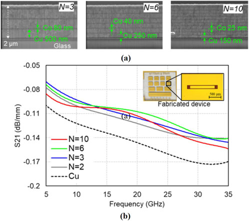
Figure 3. (A) SEM images of the Cu/Co-MC with N = 3, 6, and 10, and (B) measurement results of the N variation.
Building upon the optimized thickness conditions of tCu = 250 nm and 40 nm tCo, additional samples were fabricated to study the impact of the Cu/Co-MC ttotal on insertion loss. A ttotal based on N = 12, 6, and 3 fixed layers of the Cu/Co metaconductor were fabricated and characterized. The insertion loss plots are illustrated in Figure 4A, and a box and whisker plot based on the measurement of more than 200 samples is shown in Figure 4B. The Cu/Co-MC-based meta-interconnects exhibit an average insertion loss improvement of 0.065 dB/mm for 12P, 0.06 dB/mm for 6P, and 0.041 dB/mm for 3P at 28 GHz when compared to the solid Cu counterpart. Specifically, the average measured insertion losses of N = 12, 6, 3 of metaconductors are 0.088, 0.131, and 0.193 dB/mm at 28 GHz, while the measured insertion losses of the ttotal equivalent Cu devices are 0.153, 0.190, and 0.234 dB/mm at 28 GHz. These measurement results indicate that the thickness-optimized Cu/Co-MCs have an insertion loss below 0.1 dB/mm, meeting our target figure-of-merit and demonstrating a method of achieving better signal integrity for 112 Gbps applications. Based on these findings, it is suggested that further loss reductions can be achieved by adopting a greater number of pairs of Cu/Co-MC.
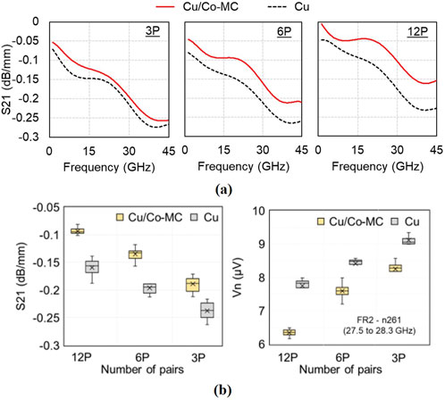
Figure 4. (A) Measured insertion loss of the Cu/Co-MC and Cu-based CPW. Fabricated CPW has a width of 106 μm and a gap of 24 μm. (B) Box plot of the measured S21 (left) and calculated noise voltage (right) (mean:
Achieving low insertion loss is crucial for long-reach interconnect signal quality, but thermal noise in lossy transmission lines also affects signal integrity, leading to distortion, skew, and timing errors. In Figure 4B, the analysis of Cu and Cu/Co-MC transmission lines in the n261 band (27.5–28.3 GHz) shows that Cu/Co-MC exhibits a lower RMS noise voltage (Vn) in the n261 band. The N = 12 Cu/Co-MC CPWs have Vn values of 6.34 μV compared to 7.88 μV for solid Cu. Similarly, for N = 6, 3 Cu/Co-MCs show lower Vn values than solid Cu counterparts. The Cu/Co-MC-based transmission line offers not only reduced insertion loss but also thermal noise improvements, enhancing the signal-to-noise ratio and lowering receiver sensitivity requirements. This makes it advantageous for high-speed data center networks and supercomputer applications.
The primary objective of this work is to demonstrate reduced conductor losses as compared to Cu at the 112 Gbps Nyquist frequency of 28 GHz. To achieve this, the study performed the first combined simulation and experimental parametric analysis to optimize Cu/Co-MCs. Achieving less than 0.1 dB/mm (0.08 dB/mm) insertion losses for 112 Gbps applications and a 42.86% reduction in conductor power losses as compared to Cu counterparts. The key foci of this study were on determining and understanding the optimal individual Cu and Co layer thicknesses and thereafter the impact of the total thickness of the conductor. Simulations predicted that small thicknesses of Cu and Co at a fixed ratio reduce conductor losses; however, experimental observations contradicted these results, providing the insight that effects of the metal-to-metal boundaries must be considered and incorporated into future research. Additionally, the simulated predictions and experimental observations of the relationship between increased total thickness and reducing conductor losses correlated well. Based on these results and to further bring MCs to the fore, there are other challenges that must be addressed. The most pressing is to address the feasibility of scaling MCs using commercial fabrication processes. Once this is determined, long-term reliability and thermal stability of the Cu/Co-MCs must be examined with a focus on the impact on signal integrity and insertion loss characteristics. Additionally, the upfront and long-term cost implications must also be addressed. It is reasonable to assume at this time that since Co is ∼2x the cost of Cu and Cu/Co-MCs will have additional fabrication complexities, these will translate to increased upfront costs, whether it is possible to offset this by long-term cost reductions or value created by performance enhancements must be established. Finally, work to characterize the electromagnetic interference characteristics of Cu/Co-MC-based devices must be analyzed beyond the simulation work conducted in Kim et al. (2023). These challenges present a path toward verifying that Cu/Co-MC is a viable conductor solution for 112 Gbps applications. In summary by means of simulated and experimentally verified parametric studies, a noteworthy target was achieved and reduction in conductor losses demonstrated in this work. Based on these results there is potential, especially in multiple serial bus configurations, for making Cu/Co-MC-based meta-interconnects a solution for high-speed data center applications and broadband (5G/6G) communication applications.
The raw data supporting the conclusions of this article will be made available by the authors, without undue reservation.
HK: Conceptualization, Data curation, Formal Analysis, Investigation, Methodology, Writing–original draft. AW: Data curation, Formal Analysis, Investigation, Writing–review and editing, Writing–original draft. RB: Conceptualization, Formal Analysis, Writing–review and editing. Y-KY: Funding acquisition, Project administration, Resources, Supervision, Validation, Writing–review and editing.
The author(s) declare that financial support was received for the research, authorship, and/or publication of this article. This work is supported in part by the Cisco University Research Program Fund, a corporate advised fund of Silicon Valley Community Foundation (Gift # 2022-246616 (3696)), NSF Convergence Accelerator Program (ITE-2235978), and NSF Engine Program (2315320) (Corresponding author: Y-KY).
This work has been supported by the Cisco University Research Program and National Science Foundation. The authors are thankful for their support and mentorship.
The authors declare that the research was conducted in the absence of any commercial or financial relationships that could be construed as a potential conflict of interest.
All claims expressed in this article are solely those of the authors and do not necessarily represent those of their affiliated organizations, or those of the publisher, the editors and the reviewers. Any product that may be evaluated in this article, or claim that may be made by its manufacturer, is not guaranteed or endorsed by the publisher.
Anon (2023). Common electrical I/O (CEI)-112G – OIF. Available at: https://www.oiforum.com/technical-work/hot-topics/common-electrical-interface-cei-112g-2/.
Bowrothu, R., Kim, H.-I., Lee, W., Clingenpeel, T., and Yoon, Y. (2022). Highly energy-efficient metaconductor-based integrated RF passives: metaconductor-based RF passives. IEEE Microw. Mag. 23 (8), 83–93. doi:10.1109/mmm.2022.3173468
Bowrothu, R., and Yoon, Y.-K. (2020). Demonstration of low loss RF conductor in ka and V bands using Cu/Fe multilayers for 5G and millimeter wave applications. 2020 IEEE/MTT-S Int. Microw. Symp. (IMS), 313–316. doi:10.1109/ims30576.2020.9223882
Clingenpeel, T., and Yoon, Y.-K. (2017). Reliability of Cu/NiFe and Cu/Ni metaconductor devices for RF applications. 2019 IEEE 69th Electron. Components Technol. Conf. (ECTC), 2205–2211. doi:10.1109/ectc.2017.182
He, R., Schneider, C., Ai, B., Wang, G., Zhong, Z., Dupleich, D. A., et al. (2020). Propagation channels of 5G millimeter-wave vehicle-to-vehicle communications: recent advances and future challenges. IEEE Veh. Technol. Mag. 15 (1), 16–26. doi:10.1109/MVT.2019.2928898
Hwangbo, S., Rahimi, A., and Yoon, Y.-K. (2018). Cu/Co multilayer-based high signal integrity and low RF loss conductors for 5G/millimeter wave applications. IEEE Trans. Microw. Theory Tech. 66 (8), 3773–3780. doi:10.1109/tmtt.2018.2840982
Hwangbo, S., Renuka, B., Kim, H.-I., and Yoon, Y.-K. (2019). Integrated compact planar inverted-F antenna (PIFA) with a shorting via wall for millimeter-wave wireless chip-to-chip (C2C) communications in 3D-SiP. 2019 IEEE 69th Electron. Components Technol. Conf. (ECTC), 983–988. doi:10.1109/ectc.2019.00154
Kim, H.-I., Jeon, S., Hsu, R., Achkir, B., and Yoon, Y.-K. (2022). Metaconductor based highly energy efficient differential striplines for 112 Gbps data bus with sub 0.1 dB/mm package insertion loss. 2022 IEEE 72nd Electron. Components Technol. Conf. (ECTC), 903–907. doi:10.1109/ectc51906.2022.00147
Kim, H.-I., Wilcher, A., Jeon, S., Pahlavan, P., Hsu, R., Achkir, B., et al. (2023). Metaconductor-based high signal integrity interconnects for 112 Gbps SerDes interface with channel analysis. 2023 IEEE 73rd Electron. Components Technol. Conf. (ECTC), 1012–1016. doi:10.1109/ectc51909.2023.00172
Kim, J., Balankutty, A., Dokania, R. K., Elshazly, A., Kim, H. S., Kundu, S., et al. (2019). A 112 Gb/s PAM-4 56 gb/s NRZ reconfigurable transmitter with three-tap FFE in 10-nm FinFET. IEEE J. Solid-State Circuits 54 (1), 29–42. doi:10.1109/jssc.2018.2874040
Kim, Y., Tam, S.-W., and Chang, M.-C. F. (2022). Millimeter-wave contactless connectors: from fundamental research to commercialization. IEEE Microw. Mag. 23 (4), 55–70. doi:10.1109/mmm.2021.3136686
Neves, A., Carrel, J., Barnes, H., Resso, M., and W. Lee, T. (2016). 32 to 56 Gbps serial link analysis and optimization methods for pathological channels. Available at: https://assets.informa.com/webcasts/Keysight_Slides_012617.pdf (Accessed January 26, 2018).
Nouri, N., Abouei, J., Jaseemuddin, M., and Anpalagan, A. (2020). Joint access and resource allocation in ultradense mmWave NOMA networks with mobile edge computing. IEEE Internet Things J. 7 (2), 1531–1547. doi:10.1109/jiot.2019.2956409
Prathiba, S. B., Raja, G., Anbalagan, S., Dev, K., Gurumoorthy, S., and Sankaran, A. P. (2021). Federated learning empowered computation offloading and resource management in 6G-V2X. IEEE Trans. Netw. Sci. Eng. 9, 3234–3243. doi:10.1109/tnse.2021.3103124
Pratt, W. P., and Bass, J. (2009). Perpendicular-current studies of electron transport across metal/metal interfaces. Appl. Surf. Sci. 256 (2), 399–403. doi:10.1016/j.apsusc.2009.06.008
Qualcomm (2018). Making 5G NR a Commercial Reality A unified, more capable 5G air interface. Available at: https://www.qualcomm.com/media/documents/files/making-5g-nr-a-commercial-reality.pdf (Accessed April, 2018).
Rappaport, T. S., MacCartney, G. R., Sun, S., Yan, H., and Deng, S. (2017). Small-scale, local area, and transitional millimeter wave propagation for 5G communications. IEEE Trans. Antennas Propag. 65 (12), 6474–6490. doi:10.1109/tap.2017.2734159
Razdan, S., De Dobbelaere, P., Xue, J., Prasad, A., and Patel, V. (2022). Advanced 2.5D and 3D packaging technologies for next generation Silicon Photonics in high performance networking applications. 2022 IEEE 72nd Electron. Components Technol. Conf. (ECTC), 428–435. doi:10.1109/ectc51906.2022.00075
Salem, A., Tripician, K., and Singaravelu, S. (2020). At speed testing challenges and solutions for 56Gbps and 112Gbps PAM4 SerDes. 2020 IEEE Latin-American Test. Symp. (LATS), 1–5. doi:10.1109/lats49555.2020.9093685
Keywords: 5G, glass, high speed interconnect, metaconductor, meta-interconnect, millimeterwave, signal integrity, skin effect
Citation: Kim H-i, Wilcher A, Bowrothu R and Yoon Y-K (2025) Cu/Co meta-interconnects for 112 Gbps high speed applications. Front. Electron. 6:1493911. doi: 10.3389/felec.2025.1493911
Received: 10 September 2024; Accepted: 27 January 2025;
Published: 14 February 2025.
Edited by:
Hui Jae Yoo, Intel, United StatesReviewed by:
Ashokkumar Srinivasan, Jawaharlal Nehru Technological University, Hyderabad, IndiaCopyright © 2025 Kim, Wilcher, Bowrothu and Yoon. This is an open-access article distributed under the terms of the Creative Commons Attribution License (CC BY). The use, distribution or reproduction in other forums is permitted, provided the original author(s) and the copyright owner(s) are credited and that the original publication in this journal is cited, in accordance with accepted academic practice. No use, distribution or reproduction is permitted which does not comply with these terms.
*Correspondence: Yong-Kyu Yoon, eWt5b29uQGVjZS51ZmwuZWR1
Disclaimer: All claims expressed in this article are solely those of the authors and do not necessarily represent those of their affiliated organizations, or those of the publisher, the editors and the reviewers. Any product that may be evaluated in this article or claim that may be made by its manufacturer is not guaranteed or endorsed by the publisher.
Research integrity at Frontiers
Learn more about the work of our research integrity team to safeguard the quality of each article we publish.