 Muhtasim Alam Chowdhury
 Mousam Hossain
 Christopher Mastrangelo
 Ronald F. DeMara2
 Soheil Salehi
- 1Department of Electrical and Computer Engineering, University of Arizona, Tucson, AZ, United States
- 2Department of Electrical and Computer Engineering, University of Central Florida, Orlando, FL, United States
Hardware-based acceleration approaches for Machine Learning (ML) workloads have been embracing the significant potential of post-CMOS switching devices to attain reduced footprint and/or energy-efficient execution relative to transistor-based GPU and/or TPU-based accelerator architectures. Meanwhile, the promulgation of fabless IC chip manufacturing paradigms has heightened the hardware security concerns inherent in such approaches. Namely, unauthorized access to various supply chain stages may expose significant vulnerabilities resulting in malfunctions including subtle adversarial outcomes via the malicious generation of differentially-corrupted outputs. Whereas the Spin-Orbit Torque Magnetic Tunnel Junction (SOT-MTJ) is a leading spintronic device for use in ML accelerators, as well as holding security tokens, their manufacturing-only security exposures are identified and evaluated herein. Results indicate a novel vulnerability profile whereby an adversary without access to the circuit netlist could differentially-influence the machine learning application’s behavior. Specifically, ML recognition outputs can be significantly swayed via a global modification of oxide thickness (Tox) resulting in bit-flips of the weights in the crossbar array, thus corrupting the recognition of selected digits in MNIST dataset differentially creating an opportunity for an adversary. With just 0.05% of bits in crossbar having a flipped resistance state, digits “4” and “5” show the highest overall error rates, and digit “9” exhibit the lowest impact, with recognition accuracy of digits “2,” “3,” and “8” unaffected by changing the oxide thickness of SOT-MTJs uniformly from 0.75 nm to 1.2 nm without modifying the netlist nor even having access to the circuit design itself. Exposures and mitigation approaches to such novel and potentially damaging manufacturing-side intrusions are identified, postulated, and quantitatively assessed.
1 Introduction
Recent advancements in hardware designs and emerging devices have shown promising potential for accelerating machine learning (ML) and neural network (NN)-driven computation (Roy et al., 2020; Cheng et al., 2021; Lu et al., 2024) Such computation requires rapid and reliable operations at the hardware level to ensure minimal loss in the algorithm accuracy. These hardware accelerators typically utilize various emerging technologies such as resistive random-access memory (RRAM), spin transfer torque magnetic RAM (STT-MRAM), spin orbit torque MRAM (SOT-MRAM), phase change memory (PCM), etc. to achieve orders of magnitude increase in speed and decrease in energy of the computations (Mishty and Sadi, 2021). Among these emerging devices, MRAM has shown to be a highly promising technology in its category, and it can be readily integrated with the traditional baseline CMOS design with minimal incurred fabrication cost. MRAM devices benefit from non-volatility, high endurance, compact cell size, and faster read and write capability. Additionally, among the several varieties of MRAM devices, SOT-MRAM has demonstrated superior performance and reliability while providing small area footprint and high density, low read and write energy, and near-zero leakage power.
Furthermore, with technological advancement in the semiconductor processing industry as well as the increased complexity of the current chip design, the cost of maintaining and creating tools for integrated circuits (IC) manufacturing has increased rapidly. Thus, the majority of IC design companies, with few exceptions, have adopted a fabless business model that utilizes a distributed global supply chain. Moreover, the globalization of the IC supply chain has resulted in the emergence of several hardware vulnerabilities and threats (Salmani and Salmani, 2018). A simplified IC supply chain process is illustrated in Figure 1, which provides an overview of the entire IC supply chain process, accompanied with potential hardware security threats. Current IC supply chain model allows adversaries to introduce malicious design modifications at various stages of the process (Hu et al., 2021). Notably, these include IP piracy, IC overuse, reverse engineering, hardware Trojan, counterfeiting and side channel attacks (Kolhe et al., 2022; Kolhe et al., 2022; Bryant et al., 2023; Gubbi et al., 2023).
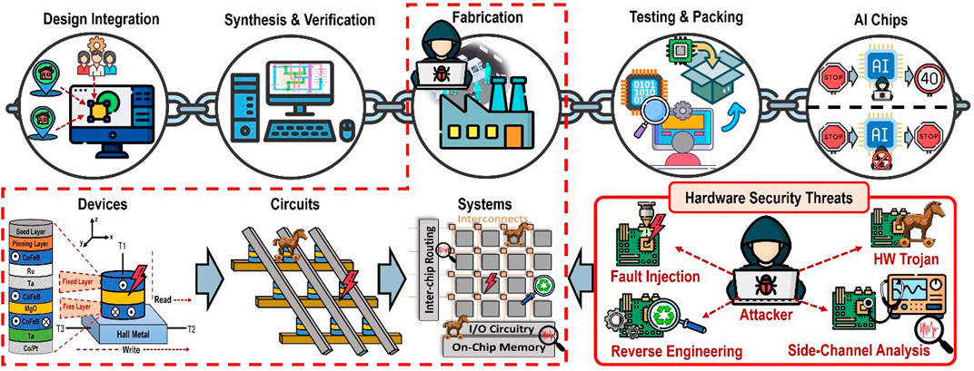
Figure 1. Simplified overview of IC supply chain process and security threats associated with the process.
Trustworthiness of the hardware platform attains significance due to exposures of authorized and unauthorized accesses during various manufacturing processes. If the security of an IC is compromised, it could result in vulnerabilities to algorithms running on the platform, as well as to other hardware components within the platform. Therefore, it is imperative to understand the supply chain exposures, especially in applications such as ML where the output behavior is intricate and well-recognized as challenging to observe and/or explain/elucidate. Currently, however, there is a gap in the research regarding the reliability of the computing operations and the security threats affecting the hardware components, including the ML hardware accelerators. Whereas in the future, when every smart device will be equipped with an AI-integrated chip (Mobile AI: On-device ai: Qualcomm Wireless Technology and Innovation, 2023), there will be a question of liability for these devices, as the AI chips will be manufactured using emerging technologies like spintronics (Barla et al., 2021). If we cannot secure the spintronics device itself, then it will cause the accelerator devices to produce incorrect outputs compared to the intended ones. As these issues persist into the future, it will lead to reliability concerns for these AI-enabled chips. Thus, it is critical to analyze such designs in order to optimize the computation speed and minimize the overhead in terms of energy and area while ensuring the security and reliability of the hardware.
In this paper, we explore the sensitivity of SOT-MTJ device behavior to the presence of various manufacturing parameter changes from the viewpoint of security. An adversary in the supply chain could intentionally modify relatively benign aspects of the MRAM manufacturing processes for SOT-MTJs, which expose vulnerabilities to a variety of more complex and stealthy attacks. Even a slight alteration in MRAM device physical parameters, such as a change in the thickness oxide layer (Tox) by a fraction of a nanometer can modify device functionality, as well as leverage unwanted behavior in the favor of an adversary.
We explore how internal changes in different layers of the device can affect its behavior, as well as the impact on the performance of the ML accelerators designed using these devices. Simulation involving detailed comparison with an ideal SOT-MRAM device is used to identify how a modified SOT-MRAM device performs under specific conditions. It is shown that a malicious global change to Tox across the wafer can introduce a gainful vulnerability to the ML recognition system. The contributions of this paper can be summarized as follows:
• A new security threat in SOT-MRAM devices that may be exploited independently of the circuit netlist.
• The paper exhibits how this vulnerability might be exploited in an attack, illustrating how differences in oxide thickness can cause ML accelerators to behave differently.
• Demonstrates the significant influence of device-level vulnerabilities on application-level performance, particularly on the precision of digit identification in machine learning models.
• Links the reported vulnerability to the MITRE Common Weakness Enumeration (CWE) database, especially referencing CWE-1248 and CWE-1384, which pertain to semiconductor faults and mishandling of physical circumstances.
• This paper offers mitigation recommendations to tackle the observed vulnerability, such as implementing countermeasures against reverse engineering and fault injection attacks. Also, the use of meta-training to enhance neural network resistance to manufacturing discrepancies.
The manuscript is organized as follows: It begins with a background presentation, followed by our proposed sensitivity analysis method in Section 3. Section 4 discusses the simulation and evaluation results. Mitigation suggestions are provided in Section 5, and the paper concludes in Section 6.
2 Background and related works
In this Section, we will first provide an overview of emerging SOT-MRAM devices followed by the threats that could potentially affect these devices using various exploits presented in the literature.
2.1 SOT-MRAM for ML accelerators
The conventional RAMs have been traditionally used for memory applications, and they are not designed to implement state-of-the-art training and learning algorithms such as Deep Neural Networks (DNNs). Recent advancements in emerging technologies have shown these devices to be promising candidates for rapid memory operations as well as logic implementation and computation (Jung et al., 2022). In particular, SOT-MRAMs have been utilized in literature to implement ML Accelerators more efficiently to achieve orders of magnitude improved energy-efficiency and speed compared to the traditional CPU or GPU-based ML implementations. Such accelerators take advantage of SOT-MRAMs to build crossbar arrays for efficient implementation of the vector matrix multiplication (VMM), which is commonly used to perform ML training and inference. Given the increase of utilizing ML accelerators in critical systems, such as autonomous vehicles and systems as well as defense and health applications, it is important to ensure confidentiality, reliability, security, availability, and integrity of these accelerators.
The SOT-MRAM devices utilize the magnetic tunneling junction (MTJ) with CMOS transistors as peripheral circuit to read and write information in the MTJs (Ali et al., 2018). The MTJ is a structure consisting of a thin oxide layer positioned between two layers of ferromagnetic material. The magnetization of the free layer within the MTJ can be altered by applying either a current or a voltage. SOT-MTJ uses two separate paths for a reliable read and write operation. As shown in Figure 2, in order to change the state of the MTJ cell from Anti Parallel (1 or high resistive state) to Parallel (0 or low resistive state), a charge current is applied to terminals T2 and T3 to perform the write operation. To determine the magnetization orientation of the free layer in the MTJ cell, a spin current due to SOT will be produced in a downward or upward direction which is perpendicular to the charge current in the HM. In order to read the value stored in an SOT-MTJs, a current is applied through terminals T1 and T2 and a sense amplifier is utilized. We used the approach given in paper (Zand et al., 2016) to simulate the behavior of SOT-MTJ devices in this paper, in which a Verilog-AMS model is built utilizing the physics equations provided in (Manipatruni et al., 2014). The model is then used in the SPICE circuit simulator to test the functionality of the constructed circuits. Additionally, (Jin et al., 2023), have demonstrated the use of high-reliability, reconfigurable, and fully non-volatile full-adders based on SOT-MTJ for image processing applications, further emphasizing the practical applications and robustness of SOT-MTJ devices in various fields.
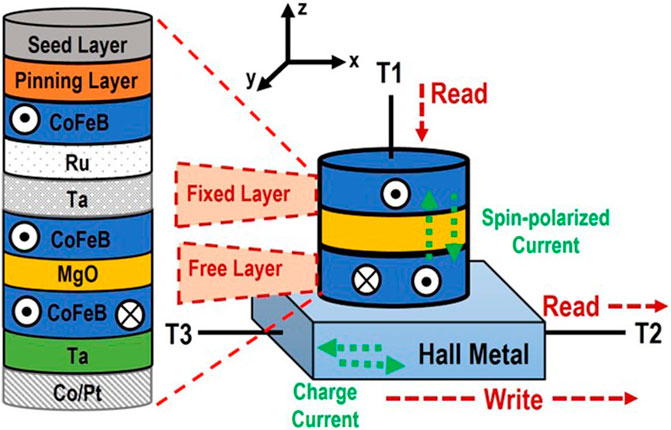
Figure 2. Device structure of an SOT-MTJ cell.
2.2 Supply chain threats on SOT-MRAM
Recent research has explored the benefits of alternatives to von-Neumann architectures using emerging devices for emerging applications such as hardware-aware intelligent edge devices as well as the application of hardware-enabled security. Considering the increased interest in using SOT-MRAMs for deploying energy-efficient computing for resource-constrained edge devices and the Internet of Things (IoT), they are an expected target for adversaries to exploit potential vulnerabilities. Below is a concise list of potential threats that could affect the integrity of the SOT-MRAM-based ML accelerator chips:
• Side-Channel and Probing Attacks: require physical access to the supply voltage and electromagnetic emission traces of the ML accelerator chip. In addition, for probing attacks locating memory components generating inputs and observing the behavior of the hardware is required.
• Reverse-Engineering Attack: ML accelerator chips are designed in a dense and modular fashion on top of the baseline CMOS devices, which makes reverse engineering challenging. With physical access to the chip, adversaries can apply inputs and observe output behavior to extract model parameters such as weights as well as their relationship with the inputs, and eventually clone the design. The modular design of the ML accelerators makes this more significant.
• Fault Injection and Focused Ion Beam Attacks: require access to the ML accelerator chip to perform fault injection (FI) attacks. The adversary needs to decapsulate the chip, locate the region of interest on the layout, apply inputs, and observe outputs’ behavior or inject voltage glitches. Additionally, without physical countermeasures in the front or backside of the chip, a focused Ion beam attack can cause random bit-flips and random faults.
• Hardware Trojan Attack: the threat of hardware Trojans (HTs) is present at various stages of the IC supply chain. HTs are malicious modifications at any stage of the design that can remain stealthy until triggered by a rare event in the design. Once triggered a payload will be deployed to degrade accuracy and performance, cause faults and failures, or leak information.
Furthermore, recent approaches have utilized SOT-MRAMs to mitigate hardware security vulnerabilities within the supply chain process (Divyanshu et al., 2022). For example, the work in (Divyanshu et al., 2023) introduces an innovative approach to generate hardware watermarks by utilizing SOT-MTJ devices, which aims to secure intellectual property (IP) cores within the context of system-on-chip (SoC) design. Considering the device-level threats on SOT-MRAM, such approaches may not result in a secure implementation of hardware. Although these works provide useful insights into vulnerabilities affecting ML accelerators using emerging devices, they do not explore the manufacturing threats to the device-level that induce significant algorithm-level impacts. Thus, herein we introduce a novel threat model, demonstrate a vulnerability in ML accelerators utilizing emerging devices such as SOT-MRAM, and provide mitigation suggestions to thwart such threats.
3 Proposed approach for sensitivity analysis
In this Section, we propose a threat model that exploits the sensitivity of device characteristics to process variation. Subsequently, we detail our approach to study the impact of such attacks at the application level.
3.1 Threat model
This Section presents the development of a threat model premised on a benign modification of critical physical parameters of the SOT-MTJ during the manufacturing process that can disrupt the device’s expected operation. A white-box threat model is devised based on the following assumptions: 1) The attacker is a hardware supply chain insider, capable of introducing variations in one or more critical MTJ parameters during fabrication; 2) the introduced variations fall within an acceptable range while maintaining a stealthy nature, making them challenging to detect; and 3) the attacker also has prior knowledge of the memory architecture of the neural network, i.e., the knowledge of the critical nodes in the weight matrix, that when affected by bit-flips can significantly affect the accuracy. These assumptions are valid due to side-channel information leakage in recent times, which can transpire if the attacker has a subset of the test data and uses it for inference. In Section 4, we provide experimental evidence that modification of device physical characteristics could leverage process variation (PV). In particular, we demonstrate how changing the thickness of the oxide layer, Tox, can result in modification of the resistive behavior of MTJs; thus, affecting the read current flowing through the device. Considering an ML accelerator design that utilizes a crossbar architecture with MTJs, such changes in the read current can accumulate across neighboring branches, resulting in incorrect firing of neurons within a neural network application. An attacker having this knowledge can determine the minimum threshold for variation for a stealthy attack, which falls within the acceptable range to pass functional testing. However, this can significantly disrupt the usual operation of a target application.
3.2 Approach to examine sensitivity against various threats
Our high-level approach to examine the sensitivity of the application against such threats is depicted in Figure 3. The goal is to introduce PV on various device characteristics and study the impact on performance of a larger in-memory computing application implemented with these devices, such as digit recognition, to demonstrate how changes in physical parameters at the device level can transcend and impact the performance at the application level. Furthermore, we analyze how read operations on few devices in a row can affect the original resistive states of the devices under process variation. It is observed that accumulated currents from multiple branches in the weight matrix, such as the read currents, Iread1 and Iread2, shown in Figure 3, may be large enough to cause either bitflips of multiple weight nodes in the crossbar array or incorrect firing of neurons in a given ANN. Such bitflips eventually affect the performance, e.g., reducing the accuracy of a handwritten digit recognition application based on the MNIST dataset.
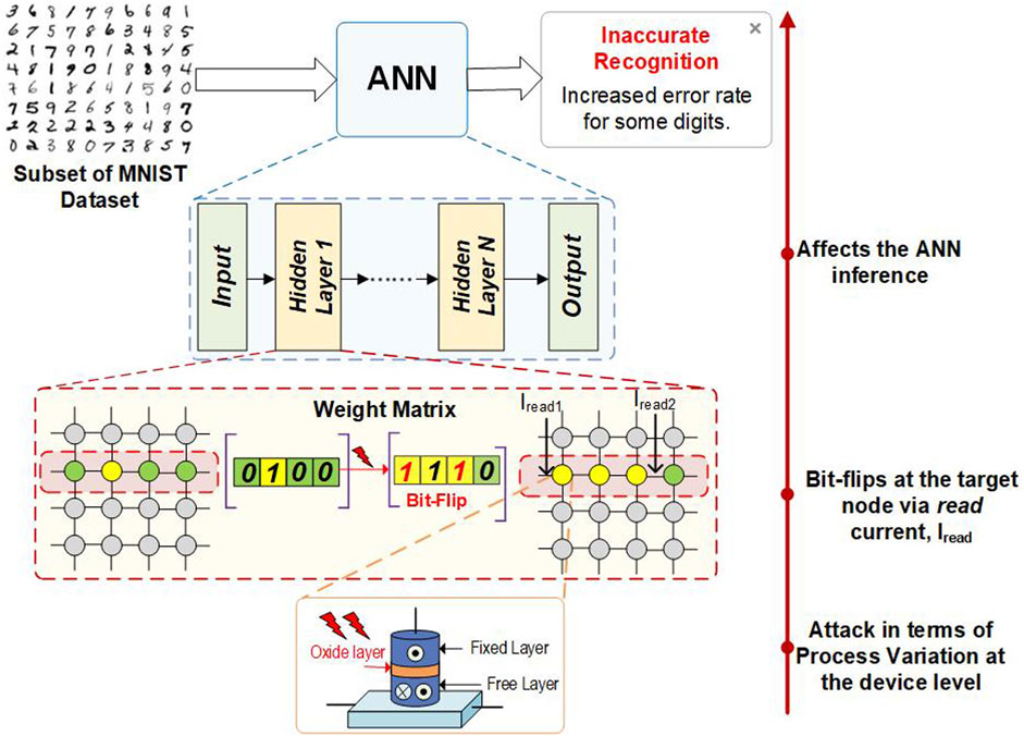
Figure 3. Approach to examine sensitivity against various threats.
For this study, we initially consider a 10% isolated variations of oxide thickness as well as length, width, and thickness of both free layer and heavy metal layer of the SOT-MTJ and observe its effect of device resistance characteristics. Furthermore, we study the combined effect of process variation on all three, i.e., the free layer length, width, and the oxide thickness parameters, by performing Monte Carlo (MC) simulations, such that the combined total variation is limited to less than 10%. We avoid exceeding this limit, since beyond this the variations in physical dimensions of the device could be detectable during the testing, violating the attack’s purpose of remaining stealthy. After careful analysis, we study the effects of PV on the switching behavior of a single device via simulation in HSPICE. Finally, we study the impacts of such variations on the performance of a hand-written digit recognition application working with the PIN-Sim framework (Ahmed et al., 2017) for intelligent inference.
4 Results and discussion
In this Section we provide the simulation results and discuss potential detection and mitigation techniques.
4.1 Tools and models used for simulation
Our evaluation framework and process flow are depicted in Figure 4. We utilize a MATLAB-based SOT-MTJ model to identify the critical device parameters, alteration of which significantly affects the device resistance characteristics. To analyze the effect of the physical variations on device performance, we utilize a HSPICE model of the SOT-MTJ device with parameters listed in Table 1 (Ahmed et al., 2017; Hossain et al., 2023; Hossain et al., 2024) along with the resistance values, i.e., high (anti-parallel (AP), and low, i.e., parallel (P), resistive states and tunnel magnetoresistance (TMR) as obtained from MATLAB simulations. We measure the read current (Iread) and the corresponding read duration of the SOT-MTJ, and study whether due to PV, the same read current can end up causing the device to switch its state within the measured read duration. Moreover, we designed a 786 × 200 × 10 ANN using the PIN-Sim framework and introduced multiple targeted bitflips in the weights and bias arrays of the ANN to study the impact on applications targeted for ML accelerators (Ahmed et al., 2017).
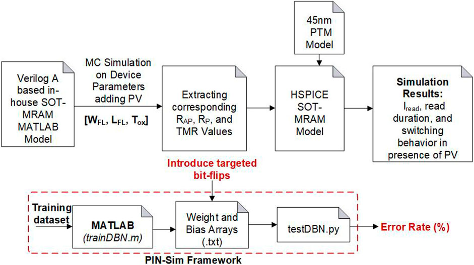
Figure 4. Simulation Framework and Process flow.
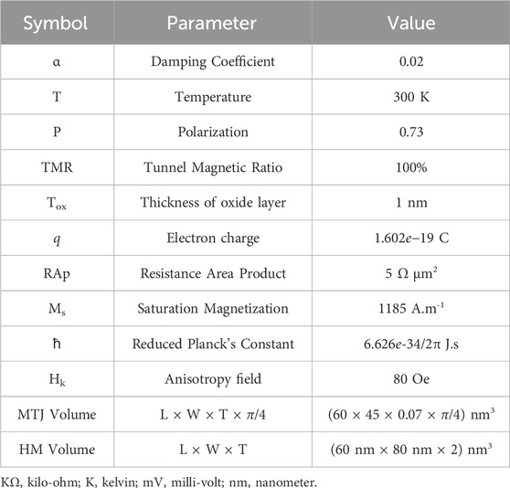
Table 1. HSPICE device simulation parameters.
4.2 Single device results
The resistance of MTJ in a SOT-MRAM is modeled using Eqs 1, 2:
where RP = RMTJ and RAP = RMTJ(1+TMR), Tox is the oxide layer thickness, f is a material-dependent parameter that depends on the resistance-area product of the device, A is the surface area of the device, φ is the energy barrier height of the oxide layer, Vbias is the bias voltage, and Vh is the bias voltage at which TMR drops to half of its initial value (Hossain et al., 2023; Hossain et al., 2024). Figure 5 shows our findings by performing MC simulations with 2,000 instances to observe the effect of isolated 10% PV of various device parameters on RP, RAP, and TMR. The effect of PV on the dimensions of the heavy metal is found to be negligible on the device resistances and the TMR, and hence not included herein. However, the length and width of the device and the thickness of oxide layer shows high dependency with the device resistive behavior and TMR, which we explore further to investigate our threat model. Figure 5A, B show that device resistive behavior has a linear proportional relation with the width (WFL) and length (LFL) of the free layer. It is found that the TMR, being a ratio of the device resistances, remains constant for both the variations. Figure 5C depicts that the device resistance increases exponentially with increase in the oxide thickness (Tox), especially beyond 1.15 nm, whereas TMR vs. Tox has a linear relationship as per Figure 5D. The TMR value of the MTJ device utilized in our simulations is 100%, as indicated in Table 1. In comparison to recent research (Chiang et al., 2020) that has reported TMR values of 250% or higher, this value is comparatively moderate. Nevertheless, it serves as a valuable baseline for assessing the effect of PV on device performance. Higher TMR values would generally result in a larger difference between the R_P and R_AP resistance states, enhancing the distinguishability of these states and potentially improving the robustness of the ML model against PV-induced errors. In the presence of PV, devices with higher TMR could exhibit reduced sensitivity to minor variations in device parameters and potentially maintain higher accuracy in ML model predictions. However, accuracy degradation can still occur in case of significant variations, resulting in increased error rates under extreme PV conditions. It can be observed that with the decrease in WFL and LFL, the gap between the resistances of the R_P and R_AP states increases. This is illustrated in Figures 5A,B, where the spread in resistance values widens as WFL and LFL decrease. Conversely, with a decrease in Tox, the gap between the resistances of the R_P and R_AP states narrows, as shown in Figure 5C. This narrowing of the resistance gap with decreasing Tox could potentially result in complications including reliability issues such as read failure, oxide breakdown, and unwanted bitflips.
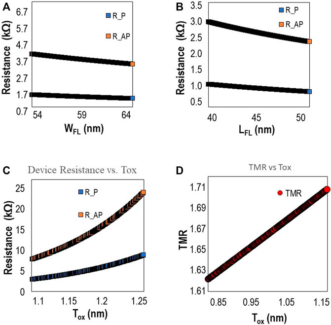
Figure 5. Individual PV analysis of (A) width of free layer, (B) length of free layer, and (C) oxide thickness on RP, and RAP, and (D) effect of oxide thickness on TMR.
Furthermore, in the scenario considering the combined effect of PV, amounting to a total 10% variation, on length, width, and thickness parameters, we observe from Figures 6A, B, that RP and RAP device resistances exhibit comparable distributions with respect to the width and length of the free layer, with multiple overlapping samples, as well as a few unexpected anomaly points that do not fall within either cluster. Such anomalies may be of particular interest to a malicious attacker seeking to exploit the unanticipated device behavior to inject faults or cause device malfunction. Figure 6C demonstrates the exponential dependence of device resistance with thickness of oxide layer, in combination with variation in width and length of free layer. Moreover, Figure 6D demonstrates the linear dependence of TMR w.r.t. variations in oxide thickness, width, and length of free layer. For the range of oxide thickness between 0.8 nm and 1.15 nm, the RP, RAP values appear to be very close, as shown in Figure 5C. Considering these results, it is valid to hypothesize that a minor variation in oxide thickness may cause a change in device resistance from RP to RAP, and vice versa, making the devices prone to faults and bitflips from Logic “0” to Logic “1.” Our experimental values of Tox, WFL and LFL lie within 96% confidence intervals of 1 nm ± 1.45e-3 nm, 60 nm ± 8.85e-11 nm, and 45 nm ± 6.65e-11 nm, respectively, for the 2,000 samples.
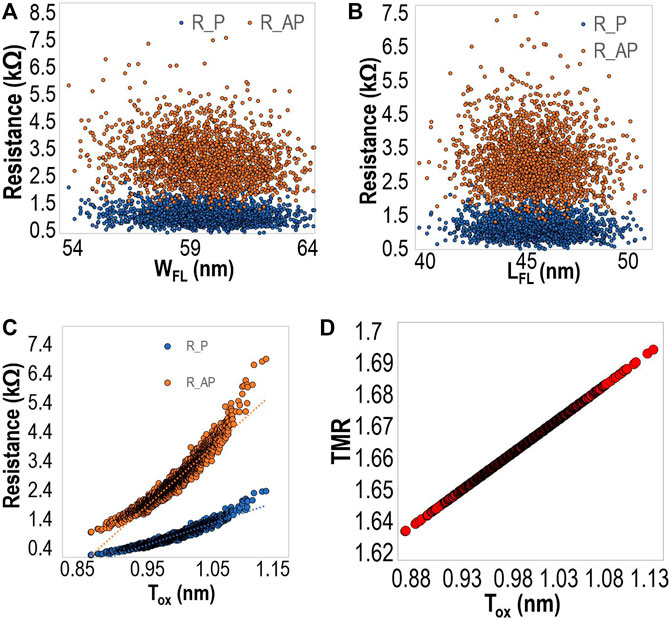
Figure 6. Applying combined PV to length, width, and thickness parameters. Effect of modification in (A) width of free layer, (B) length of free layer, and (C) oxide thickness on device resistance and (D) effect of Tox variation on TMR.
According to the SOT-MTJ model used (Hossain et al., 2023; Hossain et al., 2024), the device oxide thickness should be in the operating range of 0.85 nm–1.15 nm. Thus, we apply this as a limitation for our investigation to consider variations within −3% of 1nm, which is our baseline. First, we measure the read current that passes through the SOT-MTJ device as well as capture the read duration, with parameters listed in Table 1 for different oxide thicknesses values, by modeling the device connected with simple read-write peripheral circuitry in HSPICE designed with CMOS PTM 45 nm HP library, at VDD = 0.8V (Ahmed et al., 2017). We aim to determine whether the read current through a device is significant enough to cause bitflips in the devices affected through PV within the read duration (<5 ns). In particular, we study the effect of variation on Tox and observe if accumulated read currents from neighboring branches in the crossbar is higher than the critical switching current and can result in an undesirable switching of the device state from “P” to “AP” or vice versa during the read operation. We calculate the switching current for the device model based on (3), where q is the electron charge, ћ is the Reduced Planck constant, α is the Gilbert damping coefficient, Hk is the anisotropy field, Ms is the saturation magnetization, and V is the volume of the nanomagnet (Rakheja and Naeemi, 2012). The values of critical switching current, Icrit_sw, for “AP” to “P,” and “P” to “AP” switching of the MTJ device are shown by the dotted lines in Figure 7 as observed in HSPICE simulation and found from (Eq. 3). It aligns with the critical switching current of the device in literature and the asymmetric switching characteristics of such devices (Rakheja and Naeemi, 2012).
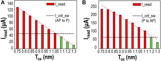
Figure 7. SOT-MTJ device read current (Iread) variation with change in oxide layer thickness during (A) “AP” to “P,” and (B) “P” to “AP” switching.
Figure 7 shows the read current values (Iread) that cause successful switching of initial state of MTJ for the particular values of Tox, and are marked in red. These represent the targeted bitflips by the attacker via introduction of malicious modifications into the MTJ device parameters. Specifically, for Tox < 1.1 nm in case of Figure 7A “AP” to “P” switching, as Iread flowing through the device is above Icrit_sw, targeted bitflips occur. Similarly, for Tox > 1.05 nm, the Iread is insufficient to cause bitflips and hence represents safe limit of Tox for such bitflip attacks through read current. Likewise, this safe range for the “P” to “AP” switching in Figure 7B is found to be Tox >1.1 nm, as the device is able to hold its initial stable resistance state and remains immune to unwanted switching.
4.3 Crossbar array results
We utilize the PIN-Sim consolidated framework developed in MATLAB, Python, and HSPICE for evaluating the performance for large scale applications. A 784 × 200 × 10 ANN is designed and trained on 3,000 training samples in MATLAB and the testing results are presented via running 100 test samples in HSPICE, containing a mixture of the ten different digits from 0–9. The training weights and biases extracted from the MATLAB-based model are translated to their corresponding memristive values in HSPICE. A python-based module is utilized to implement the memristive crossbar and a low-energy/-footprint spin-based neuron with sigmoidal activation function (Ahmed et al., 2017). The overall error rate achieved for the 100 test samples along with individual error rates for each digit recognition are listed in Table 2, where Error Rate = (# of incorrect recognitions of a digit)/(# of samples of that digit)
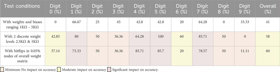
Table 2. Crossbar array analysis results - effect of bitflips on error rates (%), accuracy = (100-error rate)%.
4.4 Scope and feasibility of mitigation techniques
According to the MITRE Common Weakness Enumeration (CWE) database, the vulnerability exposed in this paper closely relates to “CWE-1248: Semiconductor Defects in Hardware Logic with Security-Sensitive Implications” and “CWE-1384: Improper Handling of Physical or Environmental Conditions.” Such weaknesses can have varying consequences. For example, based on the CWE database, CWE-1248 can result in a Denial of Service (DoS) and can be detected and mitigated during the testing phase (Common Weakness Enumeration, 2023). Although semiconductor manufacturing companies are dedicated to refining their processes continuously to minimize defects, some defects cannot be fully addressed during manufacturing. Thus, testing the silicon die utilizing fault models is paramount to detect such weaknesses. Beyond manufacturing variations, the sense amplifier circuit which is utilized to read the state of MTJ is highly susceptible to aging-related degradation of the threshold voltage of its constituent transistors. Thus, a lifetime mitigation strategy should consider Bias Temperature Instability (BTI)-induced variations which may mask or otherwise interfere with an effective vulnerability mitigation strategy (Khoshavi, et al., 2014). Furthermore, various strategies exist to safeguard ICs against threats like logic locking system, deep-learning power side-channel attack mitigation, neuromorphic computing modules for IoT, etc. (Divyanshu et al., 2022; Kolhe et al., 2022). We are currently investigating the benefits of meta-training to make the NN more resilient to manufacturing parameter variations. In addition, the accuracy of decision-making in these ML models can be influenced by the incorporation of Hardware Trojans (HTs) at the hardware level during the manufacturing process. Additionally, countermeasures such as the one proposed in (Kannan et al., 2014) have been used to prevent probing and reverse engineering attacks on ML accelerators using emerging memory devices. The various detection and mitigation strategies in literature can be classified into two broad categories:
4.4.1 Detection and mitigation of hardware Trojan attacks
Reverse-engineering is the enabler of HT attacks and some countermeasures to mitigate reverse engineering attacks are proposed in the literature (Yang et al., 2016). Some process variation mitigation techniques for spintronic and memristive devices have also been researched, such as tunable stochasticity using feedback mechanism, radiation hardening (Zhao et al., 2014). etc. Although the first method is applicable for low barrier stochastic SOT-MRAMs, a similar approach could potentially be modified to mitigate bit flips in memristive crossbars resulting from targeted Tox manipulation from adversaries to collect useful information or disrupt the proper functioning of the edge applications. The authors in (Divyanshu et al., 2022) present an approach that utilizes the spintronics device technology to showcase a secure hardware implementation that thwarts reverse engineering, hardware Trojan insertion, or IP piracy type attacks. The work in (Forte et al., 2013) puts forth a novel low overhead method for trojan identification at run-time. It leverages thermal sensors that are already present in modern systems to identify variations in power or temperature readings brought on by HT activation. In (Huang et al., 2016), a novel side-channel-aware test generation approach based on the Multiple Excitation of Rare Switching (MERS) concept is presented, which increases the HT detection sensitivity. In paper (Bao et al., 2014), the authors propose an innovative approach to use reverse engineering to identify the HT-free ICs. Adoption of one-class support vector machine, a machine learning method, helped the authors to prove a new technique to identify the HT. Finally, in (Kolhe et al., 2022), the authors propose Symmetrical MRAM-LUT (SyM-LUT) by using the LOCK&ROLL approach to eliminate the reverse-engineering and side-channel attack using a defense-in-depth mechanism, making it challenging for adversaries to insert HTs effectively.
4.4.2 Detection and mitigation of fault injection attacks
In (Tung et al., 2023), the authors present a dynamic task remapping more specifically a built-in self-test (BIST) based technique fault detection method to determine the fault density of crossbars to guide the dynamic remapping technique. Rearranging tasks with lower fault tolerance from crossbars with high fault density to ones with lower fault for training VGGs, ResNets, and SqueezeNet from scratch, ReRAM crossbar is utilized. This contributes to an average accuracy drop of only 0.85%. Another approach to detect and mitigate the FIA is being presented in paper (Muttaki et al., 2022). The authors developed a Fault-to-Time Converter (FTC), which requires a minimal overhead. To be precise, the effect of faults injected by an FI attack method is transformed into quantifiable “time” by use of the FTC sensor. After then, additional analysis of the “time” difference can be performed to determine the success of the attack. Using this FTC sensor in the FPGA platforms have shown that this design is quite effective in differentiating the various FI attack scenarios with its encoded output. In paper (Gubbi et al., 2023), the authors introduced a methodology to strengthen the timing model at design-time to account for voltage noise while training an NN, which is used as a process tracking watchdog, at test time to model the process drift while accounting for process variations. One or more of these techniques may be investigated as means towards viable mitigation approaches while incurring an overhead cost and/or increased complexity of start-up initialization procedures.
4.4.3 Variation-aware dynamic mapping mitigation strategies
ML accelerators are much more vulnerable to the manufacturing process, as process variation might alter the entire output. This variation can disrupt the reliability and consistency of these systems. To address this, one of our mitigation processes introduces the dynamic mapping technique. This technique will be used to identify and minimize vulnerabilities in ML accelerators. Our strategy acts as a compass, guiding the system to use algorithms that counteract this variation during operation. As a result, our ML systems remain robust and effective, reinforcing their reliability amidst the intricacies of their creation. The work in (Salehi et al., 2020) discusses a methodology for modeling and analyzing the impact of process variations (PV) on semiconductor memory architectures, specifically focusing on CMOS and MTJ layers used in caches and memory cells. By employing the VARIUS tool (Sarangi et al., 2008), the study simulates PV effects across the chip and evaluates their influence on memory read stability. This investigation leads to a deeper understanding of PV’s role in the reliability of hybrid SRAM and STT-MRAM last level cache memory systems. The mapping process begins with VARIUS, which generates a large pool of system maps. Static analysis tools, including R and geoR packages, are then employed to extract subtle PV parameters. These parameters play a crucial role in modeling and mapping the MTJ architecture within the crossbar array, serving as a detailed blueprint for comprehending and addressing PV-related challenges.
The mapping methodology is characterized by the generation of a PV matrix, which aids in visualizing the PV within each crossbar array. Depending on the standard deviation considered for the PV analysis of the system and the degree of variation from the VARIUS analysis, we can develop a Variation Impact Score (VIS) metric to evaluate those crossbar arrays, as well as the individual rows and columns within those arrays. These VIS are meticulously calculated using a Power-On Self-Test (POST) (Salehi et al., 2020) data and a suite of analytical tools, offering a comprehensive assessment of the impact of PV on each block. In Figure 8, a visual representation of PV mapping in the ML accelerator is illustrated using the VIS at the module-level as well as crossbar arrays. A VIS-based color region has been introduced in this figure. The VIS metric can be in a range of 1–10. In particular, scores from 1 to 3 are marked as low PV impact, 4 to 6 are marked as moderate PV impact, and anything above 6 is marked as high PV region. The architecture with low VIS is marked green, moderate is marked yellow, and high VIS is marked red.
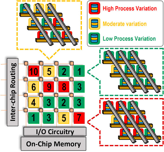
Figure 8. Visual Representation of Process Variation mapping in ML Accelerators Variation Impact Score (VIS) of crossbar arrays in the system.
For addressing the PV impacts, a mitigation approach proposed in the literature is to employ the deactivation theory of memory rows in MRAM memories (Tung et al., 2023). This approach optimizes system operations even when parts of the hardware are compromised. Such strategies involve dynamically remapping the affected areas, utilizing state-of-the-art algorithms to bypass faulty memory rows. We can use row- or column-based dynamic reconfiguration algorithms to assign ML parameters based on the PV map to result in accuracy degradation while ensuring reliability and security. Moreover, the adaptive response will preserve the robustness and integrity of the ML accelerator’s outcome. During operation, we can optimize our circuit by either bypassing the entire crossbar array or bypassing specific rows/columns based on the requirements of the matrix vector multiplication operations. This approach can assist in mitigating vulnerabilities in ML accelerators and enhance the overall system security and efficiency.
4.4.4 Discussion of limitations and future directions
To acknowledge the limitations of our study, we focus on the scope of our simulations, the assumptions made regarding process variations, and the need for experimental validation. Firstly, our simulations are based on a set of predefined parameters and assumptions, which may not fully capture the complexities and variabilities present in real-world manufacturing processes. Secondly, our work is focused on assessing TMR values only up to 100%. However, recent progress has indicated the existence of greater TMR values, which may have the capacity to modify the observed impacts of process variations. In addition, our threat model assumes an insider attacker with certain capabilities, which may not cover all potential attack scenarios. Moreover, our analysis was performed only on the MNIST dataset, and we will expand our results to include other datasets such as CIFAR10, Fashion-MNIST, KMNIST, GTSRB to provide a better understanding of such vulnerabilities. Future research should involve a more detailed and comprehensive threat model as well as the actual production of SOT-MRAM devices with deliberate process modifications to validate the simulation results and establish more effective methods for reducing potential issues. In future work, we intend to investigate the effects of greater TMR values on ML models’ robustness to PV. Specifically, we will increase the TMR value from 100% to 250% and run a series of experiments to assess the impact on device performance and ML model accuracy. With higher TMR values, it is expected to have a clear distinction between the RP and RAP resistance states, which potentially enhances the robustness of ML models against PV-induced errors. In the presence of extreme PV, increased error rates could still be observed. In order to fully understand the effects of increased TMR on the resilience of ML models to PV, it is necessary for future study to investigate these dynamics.
5 Conclusion
The recent trend of implementing SOT-MRAMs in ML accelerators obviates increasing need for awareness and eventually reasonable mitigation of security threats associated with the manufacturing process the underlying devices. It is seen that a maliciously modified SOT-MRAM can change the behavior of AI hardware performing critical decision-making tasks. In this paper, we demonstrate how global changes to a single manufacturing aspect of a SOT-MRAM device, such as Tox, can reveal bitflip vulnerability of memristive values. The simulation results illustrate a change in the oxide layers can cause unwanted switching of the operational state of the MTJ device.Beyond the simulation results showed in this paper, the fabricated MTJ device may demonstrate more vulnerabilities than the current simulation results. So, the future goal is to physically fabricate a maliciously modified MTJ device to differentially-execute operations and with the findings, the aim will be to secure the future semiconductor industry from such manufacturing threats to the sensitivity of critical device parameters.
Data availability statement
The original contributions presented in the study are included in the article, further inquiries can be directed to the corresponding author.
Author contributions
MC: Conceptualization, Investigation, Methodology, Writing–original draft, Writing–review and editing. MH: Conceptualization, Data curation, Methodology, Writing–original draft, Writing–review and editing. CM: Writing–original draft, Writing–review and editing. RD: Conceptualization, Methodology, Supervision, Writing–original draft, Writing–review and editing. SS: Conceptualization, Data curation, Investigation, Methodology, Resources, Supervision, Validation, Writing–original draft, Writing–review and editing.
Funding
The author(s) declare that no financial support was received for the research, authorship, and/or publication of this article.
Conflict of interest
The authors declare that the research was conducted in the absence of any commercial or financial relationships that could be construed as a potential conflict of interest.
Publisher’s note
All claims expressed in this article are solely those of the authors and do not necessarily represent those of their affiliated organizations, or those of the publisher, the editors and the reviewers. Any product that may be evaluated in this article, or claim that may be made by its manufacturer, is not guaranteed or endorsed by the publisher.
References
Ahmed, I., Zhao, Z., Mankalale, M. G., Sapatnekar, S. S., Wang, J. P., and Kim, C. H. (2017). A comparative study between spin-transfer-torque and spin-Hall-effect switching mechanisms in PMTJ using SPICE. IEEE J. Explor. Solid-State Comput. Devices Circuits 3 (74), 74–82. doi:10.1109/jxcdc.2017.2762699
Ali, K., Li, F., Lua, S. Y., and Heng, C. H. (2018). Area efficient shared diode multi-level cell SOT-MRAM. IEEE Trans. Magnetics 54 (11), 1–5. doi:10.1109/tmag.2018.2848114
Bao, C., Forte, D., and Srivastava, A. (2014). On application of one-class SVM to reverse engineering-based hardware trojan detection. IEEE Int. Symposium Qual. Electron. Des. 47, 54. doi:10.1109/isqed.2014.6783305
Barla, P., Joshi, V. K., and Bhat, S. (2021). Spintronic devices: a promising alternative to CMOS devices. J. Comput. Electron. 20 (2), 805–837. doi:10.1007/s10825-020-01648-6
Bryant, T., Chen, Y., Koblah, D. S., Forte, D., and Maghari, N. (2023). A brief tutorial on mixed signal approaches to combat electronic counterfeiting. IEEE Open J. Circuits Syst. 4, 99–114. doi:10.1109/ojcas.2023.3253144
Cheng, C., Tiw, P. J., Cai, Y., Yan, X., Yang, Y., and Huang, R. (2021). In-memory computing with emerging nonvolatile memory devices. Sci. China Inf. Sci. 64 (1), 221402–221446. doi:10.1007/s11432-021-3327-7
Chiang, H. L., Zhu, Z., Huang, J., Hung, S. H., Kuo, C. W., Huang, M.-H., et al. (2020). Design space analysis for cross-point 1S1MTJ MRAM: selector–MTJ cooptimization. IEEE Trans. Electron Devices 67 (8), 3102–3108. doi:10.1109/TED.2020.3005118
Common weakness enumeration (CWE) (2023). Mitre. Available at: https://cwe.mitre.org/index.html (Accessed January 17, 2024).
Divyanshu, D., Kumar, R., Khan, D., Amara, S., and Massoud, Y. (2022). Logic locking for hardware security using voltage-gated spin-orbit torque magnetic tunnel junction. IEEE Asia Pac. Conf. Circuits Syst. (APCCAS) 458, 462. doi:10.1109/apccas55924.2022.10090297
Divyanshu, D., Kumar, R., Khan, D., Amara, S., and Massoud, Y. (2023). FSM inspired unconventional Hardware Watermark using field-assisted SOT-MTJ. IEEE Access 11, 8150–8158. doi:10.1109/access.2023.3238807
Forte, D., Bao, C., and Srivastava, A. (2013). Temperature tracking: an innovative run-time approach for hardware trojan detection. IEEE/ACM Int. Conf. Computer-Aided Des. (ICCAD) 532, 539. doi:10.1109/iccad.2013.6691167
Gubbi, K. I., Saber, L. B., Srikanth, A., Sheaves, T., Beheshti-Shirazi, S. A. P. D., et al. (2023). Hardware trojan detection using machine learning: a tutorial. ACM Trans. Embed. Comput. Syst. 22 (3), 1–26. doi:10.1145/3579823
Hossain, M., Chowdhury, M. A., DeMara, R. F., and Salehi, S. (2024). Sensitivity analysis of SOT-MTJs to manufacturing process variation: a hardware security perspective. 25th Int. Symposium Qual. Electron. Des. (ISQED) 1, 1–5. doi:10.1109/ISQED60706.2024.10528782
Hossain, M., Tatulian, A., Thummala, H. R., DeMara, R. F., and Salehi, S. (2023). Energy-/Area-Efficient spintronic ANN-based digit recognition via progressive modular redundancy. IEEE Int. Symposium Circuits Syst. (ISCAS) 1, 5. doi:10.1109/iscas46773.2023.10181529
Hu, W., Chang, C. H., Sengupta, A., Bhunia, S., Kastner, R., and Li, H. (2021). An overview of hardware security and trust: threats, countermeasures, and design tools. IEEE Trans. Computer-Aided Des. Integr. Circuits Syst. 40 (6), 1010–1038. doi:10.1109/tcad.2020.3047976
Huang, Y., Bhunia, S., and Mishra, P. (2016). MERS: statistical test generation for side-channel analysis based Trojan detection. ACM Conf. Comput. Commun. Secur. 130, 141. doi:10.1145/2976749.2978396
Jin, X., Li, Y., Zhang, W., Chen, Q., Zhou, H., Zhao, M., et al. (2023). High-reliability, reconfigurable, and fully non-volatile full-adder based on SOT-MTJ for image processing applications. IEEE Trans. Circuits Syst. II Express Briefs 70 (2), 781–785. doi:10.1109/TCSII.2022.3213747
Jung, S., Lee, H., Myung, S., Kim, H., Yoon, S. K., Kwon, S. W., et al. (2022). A crossbar array of magnetoresistive memory devices for in-memory computing. Nature 601 (7892), 211–216. doi:10.1038/s41586-021-04196-6
Kannan, S., Karimi, N., Sinanoglu, O., and Karri, R. (2014). Security vulnerabilities of emerging nonvolatile main memories and countermeasures. IEEE Trans. Computer-Aided Des. Integr. Circuits Syst. 34 (1), 2–15. doi:10.1109/tcad.2014.2369741
Khoshavi, N., Ashraf, R. A., and DeMara, R. F. (2014). Applicability of power-gating strategies for aging mitigation of CMOS logic paths. IEEE 57th Int. Midwest Symposium Circuits Syst. (MWSCAS) 929, 932. doi:10.1109/MWSCAS.2014.6908568
Kolhe, G., Sheaves, T., Gubbi, K. I., Kadale, T., Rafatirad, S., Pd, S. M., et al. (2022). Silicon validation of LUT-based logic-locked IP cores. ACM/IEEE Des. Autom. Conf. 1189, 1194. doi:10.1145/3489517.3530606
Lu, A., Lee, J., Kim, T. H., Karim, M. A. U., Park, R. S., Simka, H., et al. (2024). High-speed emerging memories for AI hardware accelerators. Nat. Rev. Electr. Eng. 1 (24), 24–34. doi:10.1038/s44287-023-00002-9
Manipatruni, S., Nikonov, D. E., and Young, I. A. (2014). Energy-delay performance of giant spin Hall effect switching for dense magnetic memory. Appl. Phys. Express 7 (10), 103001. doi:10.7567/apex.7.103001
Mishty, K., and Sadi, M. (2021). Designing efficient and high-performance ai accelerators with customized STT-MRAM. IEEE Trans. Very Large Scale Integration (VLSI) Syst. 29 (10), 1730–1742. doi:10.1109/tvlsi.2021.3105958
Muttaki, M. R., Zhang, T., Tehranipoor, M., and Farahmandi, F. (2022). Ftc: a universal sensor for fault injection attack detection. IEEE Int. Symposium Hardw. Oriented Secur. Trust (HOST) 117, 120. doi:10.1109/host54066.2022.9840177
Qualcomm Wireless Technology & Innovation (2023). Mobile AI: on-device AI. Available at: https://www.qualcomm.com/products/mobile/snapdragon/smartphones/mobile-ai (Accessed February 21, 2024).
Rakheja, S., and Naeemi, A. (2012). Graphene nanoribbon spin interconnects for nonlocal spin-torque circuits: comparison of performance and energy per bit with CMOS interconnects. IEEE Trans. electron devices 59 (1), 51–59. doi:10.1109/ted.2011.2171186
Roy, K., Chakraborty, I., Ali, M., Ankit, A., and Agrawal, A. (2020). In-memory computing in emerging memory technologies for machine learning: an overview. ACM/IEEE Des. Autom. Conf. (DAC) 1, 6. doi:10.1109/dac18072.2020.9218505
Salehi, S., Khoshavi, N., and DeMara, R. F. (2020). Mitigating process variability for non-volatile cache resilience and yield. IEEE Trans. Emerg. Top. Comput. 8 (3), 724–737. doi:10.1109/TETC.2018.2799005
Salmani, H., and Salmani, H. (2018). “The global integrated circuit supply chain flow and the hardware trojan attack,” in Trusted digital circuits: hardware trojan vulnerabilities, prevention and detection (Springer), 1–11. doi:10.1007/978-3-319-79081-7_1
Sarangi, S. R., Greskamp, B., Teodorescu, R., Nakano, J., Tiwari, A., and Torrellas, J. (2008). VARIUS: a model of process variation and resulting timing errors for microarchitects. IEEE Trans. Semicond. Manuf. 21 (1), 3–13. doi:10.1109/TSM.2007.913186
Tung, C. H., Joardar, B. K., Pande, P. P., Doppa, J. R., Li, H. H., and Chakrabarty, K. (2023). Dynamic task remapping for reliable CNN training on ReRAM crossbars. IEEE Des. Automation Test Eur. Conf. Exhib. (DATE) 1, 6. doi:10.23919/date56975.2023.10137238
Yang, C., Liu, B., Li, H., Chen, Y., Barnell, M., Wu, Q., et al. (2016). Security of neuromorphic computing: thwarting learning attacks using memristor's obsolescence effect. IEEE/ACM Int. Conf. Computer-Aided Des. (ICCAD) 1, 6. doi:10.1145/2966986.2967074
Zand, R., Roohi, A., Fan, D., and DeMara, R. F. (2016). Energy-efficient nonvolatile reconfigurable logic using spin hall effect-based lookup tables. IEEE Trans. Nanotechnol. 16 (1), 1–43. doi:10.1109/tnano.2016.2625749
Keywords: hardware supply chain security, emerging switching devices, machine learning accelerators, SOT-MRAM, semiconductor fabrication
Citation: Chowdhury MA, Hossain M, Mastrangelo C, DeMara RF and Salehi S (2024) S-Tune: SOT-MTJ manufacturing parameters tuning for securing the next generation of computing. Front. Electron. 5:1409548. doi: 10.3389/felec.2024.1409548
Received: 30 March 2024; Accepted: 22 July 2024;
Published: 07 August 2024.
Edited by:
Ramtin Zand, University of South Carolina, United StatesReviewed by:
Mehrdad Morsali, New Jersey Institute of Technology, United StatesMehran Mozaffari Kermani, University of South Florida, United States
Copyright © 2024 Chowdhury, Hossain, Mastrangelo, DeMara and Salehi. This is an open-access article distributed under the terms of the Creative Commons Attribution License (CC BY). The use, distribution or reproduction in other forums is permitted, provided the original author(s) and the copyright owner(s) are credited and that the original publication in this journal is cited, in accordance with accepted academic practice. No use, distribution or reproduction is permitted which does not comply with these terms.
*Correspondence: Muhtasim Alam Chowdhury, bW1jN0Bhcml6b25hLmVkdQ==
†These authors have contributed equally to this work and share first authorship