
94% of researchers rate our articles as excellent or good
Learn more about the work of our research integrity team to safeguard the quality of each article we publish.
Find out more
REVIEW article
Front. Electron., 12 September 2023
Sec. Bioelectronics
Volume 4 - 2023 | https://doi.org/10.3389/felec.2023.1250655
 Sofia Drakopoulou1†
 Francesc Varkevisser2†
 Linta Sohail1†
 Masoumeh Aqamolaei2†
 Tiago L. Costa2*
 George D. Spyropoulos1*
Responsive neuromodulation is increasingly being used to treat patients with neuropsychiatric diseases. Yet, inefficient bridges between traditional and new materials and technological innovations impede advancements in neurostimulation tools. Signaling in the brain is accomplished predominantly by ion flux rather than the movement of electrons. However, the status quo for the acquisition of neural signals is using materials, such as noble metals, that can only interact with electrons. As a result, ions accumulate at the biotic/abiotic interface, creating a double-layer capacitance that increases impedance and negatively impacts the efficiency of neural interrogation. Alternative materials, such as conducting polymers, allow ion penetration in the matrix, creating a volumetric capacitor (two orders of magnitude larger than an area-dependent capacitor) that lowers the impedance and increases the spatiotemporal resolution of the recording/stimulation. On the other hand, the increased development and integration capabilities of CMOS-based back-end electronics have enabled the creation of increasingly powerful and energy-efficient microchips. These include stimulation and recording systems-on-a-chip (SoCs) with up to tens of thousands of channels, fully integrated circuitry for stimulation, signal conditioning, digitation, wireless power and data telemetry, and on-chip signal processing. Here, we aim to compile information on the best component for each building block and try to strengthen the vision that bridges the gap among various materials and technologies in an effort to advance neurostimulation tools and promote a solution-centric way of considering their complex problems.
Electrophysiology is an exciting branch of physiology that uses techniques to trace the ion flux in biological tissues and reveal information about intra- and inter-organ communication (Oken, 1996). The first study of bioelectricity, by Luigi Galvani in the 18th century, awakened the interest in interactions between electricity and biological tissues (Lüderitz, 2003). Approximately a century later, in 1901, Willem Einthoven first recorded an electrocardiogram (ECG) signal with a rather spacious device and his limbs being immersed in jars of salt solution (Barold, 2003). Since then, our interest in bioelectronics solidified and research toward various devices that interact electrically with the body increased rapidly. Inevitably, the brain, being perhaps the most interesting organ of our body, has attracted a significant amount of attention in the field.
The brain consists of billions of neurons responsible for communication within our body. Neurons communicate with each other by action potentials that travel down their axons to release neurotransmitters (Kandel, 2000). These action potentials are generated by the movement of ions inside and outside each cell, which occurs at a millisecond scale (Oken, 1996). This movement is responsible for the electricity produced by our body and the brain. Electrophysiology aims to capture these signals by placing an electrode near or inside the biological tissue of interest, such as the neural tissue. This method can provide real-time tracing of physiological events, which can reveal important information about physical processes and conditions at the time of their occurrence.
With that premise, scientists, physicians, and engineers have made great strides in researching novel materials, miniaturized devices, and methods (often developed hand-in-hand with technology) not only to record but also to interfere with signals, creating new avenues for diagnosis and treatment of physiologically relevant disorders (Chen et al., 2017; Rivnay et al., 2017; Jastrzebska-Perfect et al., 2020a; Bianchi et al., 2022).
These interdisciplinary efforts have led to several methods and devices that have been extensively used in preclinical models to reveal specific organ processes or neural dynamics under various circumstances, or clinically to help identify relevant disorders or sensory dysfunctions and mitigate them. Some of the most well-known techniques used are electrocardiography (a recording of electrophysiology from cardiac muscle; ECG), electromyography (from muscle; EMG), and brain recordings, which can be classified based on their invasiveness as EEG or intracranial EEG (iEEG)/electrocorticography (EcoG) (Duskalov et al., 1998; Teplan, 2002; Farina et al., 2004). Along with these techniques, specific instruments have been developed to record relevant activity in a hospital environment or a research laboratory. Even though this review focuses on brain interfaces and neuroelectronics, we cannot overlook some of the most successful bioelectronic devices, such as the pacemaker and the cochlear implant. Built to interface with the heart, the pacemaker was the first device to be implanted in humans in 1958, and since then, more than 600,000 pacemakers are implanted yearly (Aquilina, 2023). Then, 4 years later, cochlear implants were implanted in human ears and have emerged as one of the most successful neural interfaces to date, treating more than one million patients living with deafness (Zeng, 2022). After these devices paved the way, it was in 1987 that a deep brain stimulator was first implanted in humans to help with Parkinson’s disease, epilepsy, and other neurological diseases through electrical recordings and stimulation (Lee et al., 2019).
Neuroelectronic devices have several functional parts that, for the sake of better understanding and review, we will separate into four parts, as illustrated in Figure 1:
o Front end
o Back end/processing unit
o Interconnection and connection strategies
o Energy and data telemetry
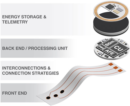
FIGURE 1. Conceptual figure showing the basic building blocks of a neural interface.
Each of these sections has specific requirements that scientists and engineers must consider during the design and development process.
The front end of a neuroelectronic device consists of interfaces (electrodes or devices) that are in immediate contact with biological tissues with which they interact electrically. Their interaction is governed by a trade-off between invasiveness and resolution (Schwartz et al., 2006). In the specific case of a brain recording, the further we place the interfaces from the neural tissue, such as in minimally invasive EEG where they are placed on the scalp, the more likely we are to record oscillations and rhythms resulting from multiple neurons and networks (Hejazi et al., 2021). Therefore, EEG shows low invasiveness but also a limited resolution. In more invasive techniques such as iEEG/ECOG, interfaces are placed closer to the neural tissue on the cortex, and resolution increases, allowing for the recording of action potentials from single units. Furthermore, using depth electrodes, we can reach single units deeper in the brain (and therefore increased resolution), but this comes at the expense of further increased invasiveness. Beyond the physical barriers that placement methods can impose on specific techniques, materials, architecture, and post-processing are critical in identifying the spatiotemporal resolution of a front-end interface.
The back end serves as the computational heart or the processing unit of a neuroelectronic device. It is often implemented as the application-specific integrated circuit (ASIC) in complementary metal–oxide semiconductor (CMOS) technology, and its design requires trade-offs between the circuit area and energy consumption that can produce miniaturized units (Zhou et al., 2018; Liu et al., 2020; Shin et al., 2022; Topalovic et al., 2023). The processing unit collects and processes data from the front-end interfaces to save them in an internal storage unit, transfer them to external centers/databases, or, if the neuroelectronic device is implemented in a closed-loop manner rather than an open-loop manner, send signals back to the front end to modulate neural activity.
Front-end and processing units should connect efficiently with minimal losses and good hermeticity (Hassler et al., 2011). However, complexities may arise as these two parts consist of various substrates and materials that have different properties and encapsulation requirements (Jastrzebska-Perfect et al., 2020a). An efficient interconnection method should consider all these and enable a connection that does not significantly increase the overall size and sacrifice the form factor.
As active electronics, neuroelectronic devices consume energy. This consumption occurs at their processing unit or during stimulation. In the specific case of chronic implants (a device enclosed in the body), energy must be provided to the system continuously during operation or stored in an internal battery for later use (Lee et al., 2015). Wireless energy transfer methods (light, sound, RF, and EM) are the best candidates for this procedure because cable use is naturally impractical (Jastrzebska-Perfect et al., 2020a). To achieve this, engineers and developers should overcome challenges that lie in potential charging losses, trade-offs between energy/data storage capacity and size, and thermal dissipation (Bazaka and Jacob, 2012; Amar et al., 2015). In the case of an open-loop implantable device, data storage and telemetry are critical, and efficient data transmission should be ensured.
According to the aforementioned, every part of a neuroelectronic device has its own desirable properties and challenges that engineers, scientists, and physicians must overcome to design the most efficient building blocks possible. Often, the properties and challenges of one part differ from those of another, and therefore, there are no one-size-fits-all solutions concerning materials, fabrication methods, and circuit implementations. In recent years, significant steps have been taken toward scientific interdisciplinarity with funding schemes and opportunities that promote such research (European Commission, 2023; Fonds Wetenschappelijk Onderzoek, 2023; Human Frontier Science Program, 2023). However, this interdisciplinarity typically occurs at the interface between different fields, such as medicine and engineering. Although interdisciplinary thinking often occurs across various fields, it is rare to see such thinking applied to diverse technologies and methods within a specific field. In many cases, academic endeavors promote a technology agenda that prioritizes one’s previous work. As a result, scientists and engineers from different technological and material backgrounds are seldom open to alternative solutions. In this review, we present the fundamentals of designing each block of a neuroelectronic device and promote a solution-centric way of thinking that focuses on overcoming challenges in the best way possible, outside of specific technology agendas.
When an action occurs in our environment, we perceive this as a sensory input of information through our senses. This event is captured by our sensory organs and then transmitted through the nerves to different brain sensory areas. These areas interact with the brain's motor areas and send back reaction information to motor nerves. The cells responsible for the communication of the nervous system and the rest of the body are neurons. Our nervous system consists of hundreds of billions of neurons that communicate in both electrical and chemical ways (Kandel, 2000).
Neurons consist of the soma, the dendrites, axons, and axon terminals. The soma or cell body contains the cell nucleus and organelles. The dendrites, branch-like structures that project out of the soma, gather information in the form of neurotransmitters from other cells and convey that to the soma. The axon, a fiber-like structure with variable length (up to 1 m), is responsible for sending information to the axon terminal to be perceived by the next neuron. This information is transmitted electrically/chemically, with action potentials and neurotransmitters. The membrane potential, the electrical potential difference between the inside of the cell and its environment, at rest is approximately −70 mV. Responsible for this charge difference between the inside and outside of a neuron are mainly sodium and potassium ions, which move across the membrane through ion pumps and ion channels. When a stimulus large enough to reach −55 mV is achieved, the voltage-gated sodium channels open and sodium ions rush in depolarizing the cell and initiating an action potential. This starts a chain reaction that triggers neighbor channels, and potential difference travels down the axon. When action potentials reach the terminal (or synapse), they trigger the neurotransmitter release. These neurotransmitters can be excitatory or inhibitory to convey to the next cell the appropriate information. Thus, in the chemical synapse, we have electrical signals converted to chemical signals in the presynaptic neuron and back to electrical signals for the post-synaptic neuron. The important information in the aforementioned abstract of neuron operation is that the movement of ions is responsible for all electrical events in neurons and is, therefore, the key to every communication in our body (Bean, 2007).
In electrophysiology, we apply electrodes or devices near neurons or neural networks to trace or modulate their electrical activity (in vitro, electroactive cells; or in vivo, biopotential). In the frequency regime, these events typically span from mHz (in ECG) up to tens of kHz (in EMG), while in amplitude from several μV up to several mV. The electrical activity of the brain (brain oscillations) can be generated by the synchronous activity of many neurons (local field potential, LFP) or the asynchronous activity of individual neurons (as we referred to previously, action potential or otherwise known as spikes). Spikes are high-frequency neural oscillations (∼1 kHz), with their amplitude depending on the recording method (μV to mV) (Gold et al., 2009; Dipalo et al., 2017). LFPs’ frequency ranges between 1 and 200 Hz, and each frequency set can reveal information regarding the underlying brain functions. For instance, alpha oscillations (8–13 Hz) are associated with attention (Klimesch, 2012), gamma oscillations (30–100 Hz) are correlated with attention and perception (Buzśaki and Wang, 2012), and delta oscillations (1–4 Hz) are considered to play a role in memory consolidation (Uguz et al., 2017). Other types of oscillations include theta (4–8 Hz), beta (13–30 Hz), and high-frequency oscillations (>200 Hz), each a result of specific characteristics and functions (Groppe et al., 2013).
When we apply an electrode near tissue or neurons, communication among them is mediated by ion flow. To have a better understanding of the general communication mechanism, we review the interface between electrodes and the electrolyte (a simplified version of tissue with plenty of mobile ions). For efficient communication, the coupling between the electronic current in the electrodes and the ionic current in the electrolyte must be maximized (Daniel, 2008). At the metal–electrolyte (corresponding to electrode–tissue) interface, electrical communication can mainly occur by Faradaic (with Faradaic electrodes and charge transfer) or non-Faradaic (with non-Faradaic electrodes and double layer charging) processes (Figure 2A (Cogan, 2008; Berggren and Malliaras, 2019). For bio-applications, we mainly prefer non-Faradaic or ideally polarizable electrodes because the electrochemical side products that result from Faradaic electrodes and relevant processes can be harmful (Bredas and Marder, 2016).
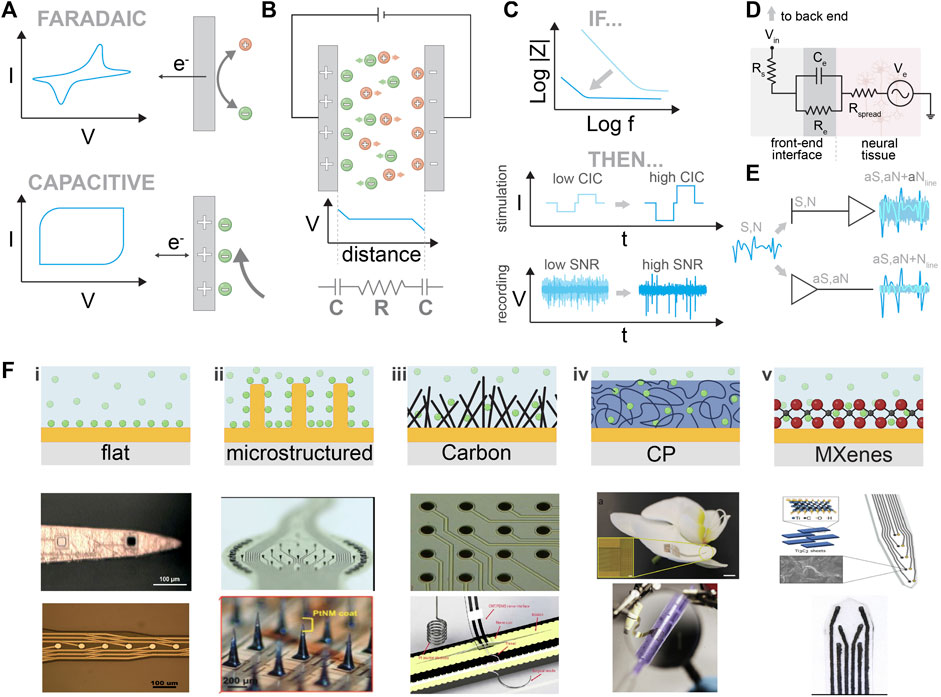
FIGURE 2. Front-end materials and interfaces. (A) Comparison between Faradaic and capacitive processes. Schematic explanation of the charge transport and charge transfer. (B) Upper part: illustration of the steady state when two metallic plates are immersed in the electrolyte. Lower part: the equivalent circuit represents the two double layers that are formed at each electrode/electrolyte interface, and the resistor represents the electrolyte. (C) Upper part: the outcome of impedance optimization in stimulation and recording electrodes. Lower part: the resulting stimulation profile for a given biphasic current pulse and recording quality of SNR is shown for a flat electrode (light blue) and for an electrode with an enhancing coating (dark blue). (D) Probe/ tissue interface equivalent circuit. For simplicity, the recording is assumed where neurons act as a voltage source (Ve). Nonetheless, the stimulation circuit can also be represented similarly. (E) Use of transistors for neural recordings. Comparison between passive and active electrodes. N is the biological noise, S is the neurophysiological signal, and Nline is the line noise. aS, aN, and Nline correspond to the amplified signals. (F) Nanostructured traditional electrode materials. Comparison between flat, nanostructured carbon, conductive polymers, and MXenes. i) Optical image of Au and Ir-plated electrode sites before the pulse test experiment. Reproduced from (Fomani A and Mansour, 2011), with permission from Elsevier B.V. Microscope image demonstrating the crossover of metal layers and electrode sites. Reproduced from (Mercanzini et al., 2008), with permission from Elsevier B.V. ii) Macroscopic image of an MEA and of a single microelectrode (Ø 50 μm, height ∼50 μm). The pillars exhibit parylene C side insulation, and their heads were wet etched and coated with TiN. Reproduced from (Steins et al., 2022), licensed CC-BY-4.0. Magnified view of the array with SiMNs with a tapered shape with a height of approximately 300 μm and sharp tips coated with PtNM. Reproduced from (Lee SH. et al., 2022), with permission from Wiley-VCH GmbH. iii) Optical micrograph of a multielectrode array device made with carbon-nanotube-based pillars. Reproduced from (Ben-Jacob and Hanein, 2008), with permission from The Royal Society of Chemistry. Freestanding CNT/PDMS nerve interface. Reproduced from (Terkan et al., 2020), licensed CC-BY-4.0. iv) A flexible organic electronics-based implant structure conforms to the surface of an orchid petal (scale bar, 5 mm). Reproduced from (Khodagholy et al., 2015b), with permission from Springer Nature America, Inc. MuSA device wrapped around a pipette. Reproduced from (Vomero et al., 2020b), with permission from Elsevier Ltd. v) Ti3C2/Au intracortical electrode array. Reproduced from (Driscoll et al., 2018), with permission from American Chemical Society. High-throughput manufacturing of the MXene ink-infused electrode array. Reproduced from (Driscoll et al., 2021), with permission from The American Association for the Advancement of Science.
To better understand the main concepts that govern the interface between non-Faradaic electrodes and tissue, we will review the ideal case of two ideally polarizable electrodes immersed in an electrolyte Figure 2B (Bredas and Marder, 2016). When a potential difference between those two electrodes is applied, ions will flow toward the electrodes. Negative ions will accumulate at the interface with the anode, while positive ions will accumulate at the interface with the cathode. At a steady state, a capacitor is formed at each electrode–electrolyte interface, consisting of an accumulation of electronic charges in the metal, compensated by ionic charges in the electrolyte. This capacitor is called the double-layer capacitor. We can model this setup with an equivalent circuit consisting of two capacitors (corresponding to the two electrode/electrolyte interfaces) and a resistor (that represents the electronic resistance of the electrolyte) (Bredas and Marder, 2016). An applied voltage across this circuit will cause a voltage drop at the resistors and capacitors. Therefore, we have
V = Vresistor + Vcapacitor =
where t is the time. If the neuron produces a time-varying flow of ions that corresponds to an AC current
where j is the imaginary unit (
As a result, the complex impedance equals
The second term (the electrode–electrolyte interface) can be minimized by increasing the capacitance (C). Similar equations for stimulation can be extracted (Figure 2C) (Bredas and Marder, 2016).
In the real case scenario, when an electrode interfaces a tissue, the equivalent circuit can be modeled as shown in Figure 2D, where Ve signifies the electrical potential generated by neurons and Rspread describes the resistance of the extracellular space and depends on the geometry of the electrode. Re and Ce refer to the leakage resistance and the electrical double-layer capacitance of the electrode/tissue interface, respectively. Finally, Rs is the resistance due to the interconnections. For a non-Faradaic or ideally polarizable electrode, the leakage resistance (Re) is high, meaning the impedance value is again determined mainly by the capacitance (Rivnay et al., 2017). In the case of implantation in actual tissue, an additional impedance element due to neuroinflammatory response should be added Figure 3B. Strategies to minimize the neuroinflammatory response and increase the quality of the recording/stimulation are discussed in detail in Section 2.2.
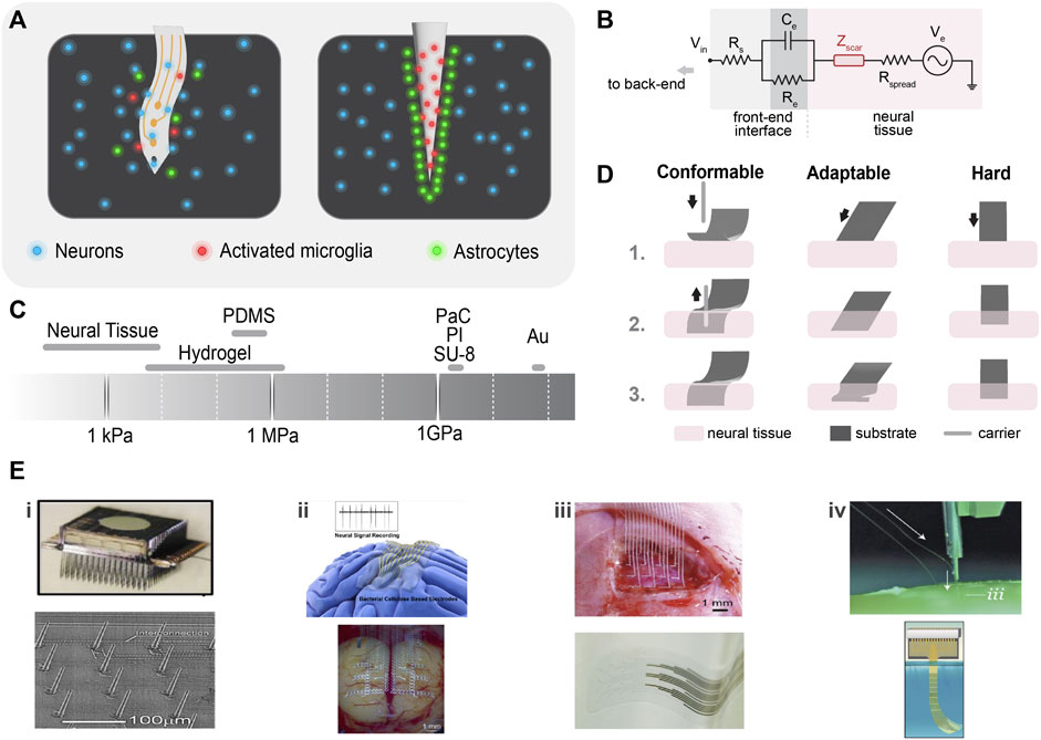
FIGURE 3. Neural interface substrates. (A) Physiological response to neural probe insertion: disruption of the blood–brain barrier and activation of glial cells (microglia and astrocytes) (left), and glial cells encapsulate the probe and form a dense scar around it compromising the probe’s performance (right). (B) Tissue/probe electrical interface: neuroinflammatory response introduces a scar impedance (Zscar) and influences the local electrical impedance. (C) Young’s modulus of tissue and common soft and hard materials. (D) Mechanical compliance of soft and hard probe materials: very conformable material (e.g., PaC) requires a carrier to be inserted in the neural tissue (left), adaptable materials (like; thermoplastics) are hard outside and become soft in the physiological environment, facilitating ease of insertion (middle), and hard materials are easy to be implanted and show mechanical compliance if made thinner (right). (E) Examples of strategies to improve tissue/probe biocompatibility; i) array of vapor–liquid–solid (VLS) silicon electrodes. Reproduced from (Goryu et al., 2012), with permission from IOP Publishing. Rigid needle-like Utah electrodes. Reproduced from (Najafi et al., 2021) licensed CC-BY-NC-ND 4.0. ii) Bacterial cellulose is being used as a super soft neural interfacing material. Reproduced from (Yang et al., 2018), with permission from American Chemical Society. Off-stoichiometry thiol-eneepoxy (OSTE+) thermosets show outstanding mechanical properties and conformability to the brain. Reproduced from (Borda et al., 2023b), licensed CC-BY-4.0. iii) Printed stretchable metal arrays retain electrical and mechanical stability. Reproduced from (Dong et al., 2021) with permission from Wiley-VCH GmbH. Low-impedance, transparent PEDOT: PSS electrode arrays were fabricated on PaC. Reproduced from (Dijk et al., 2022), licensed CC-BY-4.0. iv) A neurosurgical robot capable of inserting 192 electrodes per minute. Reproduced from (Musk, 2019), licensed CC-BY-ND-4.0. A neurotassel consists of an array of flexible and high–aspect ratio microelectrode filaments. Reproduced from (Guan et al., 2019), licensed CC-BY-NC-4.0.
Small electrodes enable high spatial resolution and recordings for individual neurons; however, as we discussed previously, in traditional electrodes, impedance values are determined by the double-layer capacitance, which is area-dependent. Therefore, the key challenge in electrode design is to maximize capacitance per unit area, or in other words, “How do we maximize Ce while keeping small electrodes?”. In the following paragraphs, we discuss the main approaches used to address this challenge.
Metal electrodes made of Pt, Ir, and IrOx have been extensively used (Robblee et al., 1985; Beebe and Rose, 1988; Rose and Robblee, 1990). Usually, due to standardized deposition methods, their surface is relatively flat (Figure 2Fi), limiting their interface with neural tissue to that of the exact area of the electrode. At this interface an area dependent capacitance is formed (∼5 μF/cm2) which negatively affects impedance (Z), charge injection capacity (CIC), and the maximal reversible charge density of electrodes, deteriorating the quality of the recording and neurostimulation (Bredas and Marder, 2016). Capacitance has a positive correlation with the exposed electrode area. Considering this, scientists and engineers have introduced new fabrication strategies that apply microstructuring to increase the surface that interacts with neural tissue (Minev et al., 2013; Obien et al., 2015; Airaghi Leccardi et al., 2019; Vachicouras et al., 2019; Lee SH. et al., 2022) (Figure 2Fii). Such microstructured surfaces enable an improved interaction with neural tissue with lower impedance and increased CIC. However, microstructuring can reach a limit imposed by the engineering methods that are used (Takeuchi et al., 2004). To further increase the effective surface area, different ways of surface modification have been proposed by changing the deposition processes or surface functionalization. Zeng and coworkers developed a series of Pt nanostructures including the nanocone (Zeng et al., 2022), nanoflower (Zeng et al., 2019; Zeng et al., 2021), nanoleaf, and nanowire (Huang et al., 2020; Huang et al., 2021).
Another way of improving electrode performance is by functional coatings. Some examples of the most promising functional coatings are listed in the following paragraphs.
Carbon-based materials such as carbon nanotubes (CNTs), carbon fibers, and graphene have gained considerable attention in neural engineering due to their high mechanical strength, flexibility, electrical conductivity, and biocompatibility. They increase the charge injection capacitance by increasing the surface area of the flat electrodes (Figure 2Fiii) (Vomero et al., 2017; Nimbalkar et al., 2018). CNTs have been implemented in micro-electrode arrays to increase recording sensitivity and longevity (Ben-Jacob and Hanein, 2008; Keefer et al., 2008; Ruhunage et al., 2023). Yoshida Kozai et al. (2012) fabricated ultrasmall and flexible organic electrical microelectrodes with a subcellular cross-sectional dimension that not only allows chronic implantation but also enables single-neuron recording. Graphene is another form of carbon-based material that can improve the SNR of neural electrodes and promote cell adhesion (Chen et al., 2013; Rastogi et al., 2017; Lim et al., 2023). Researchers have taken advantage of the transparent nature of graphene to create neural electrodes that enable both optical and electrophysiological recordings (Kuzum et al., 2014; Park et al., 2014). Other applications of carbon-based neural interfaces have been studied (Ansaldo et al., 2011; Baranauskas et al., 2011; David-Pur et al., 2014; Vitale et al., 2015; Vomero et al., 2020a; Tang et al., 2020; Hejazi et al., 2021).
Another way to increase the electrode performance is to use soft materials that allow the facile penetration of ions at the molecular scale (volumetric capacitance). Conductive polymers (CPs) have been found to have widespread applications in biomedicine, enhancing the electrical characteristics of neural devices (Green and Abidian, 2015). These advancements enable chronic implantation and have found a way toward promising products (Musk, 2019). The ability to reduce the electrode’s impedance and increase CIC (1–15 mC/cm2) is the key factor that strengthens their performance (Cogan, 2008; Stavrinidou et al., 2013). Moreover, CPs can act as a tissue–electrode intermediary balancing the mechanical mismatch and reducing the neuroinflammatory response, thus enabling long-term and stable brain activity recordings (Tybrandt et al., 2018). The most common conductive polymers used for neural applications are polyaniline, polypyrrole (PPy), and poly(3,4-ethylenedioxythiophene) (PEDOT) due to their ease of deposition, patterning, hygroscopic nature, and excellent conductive properties. The pioneer in introducing the CPs onto metallic electrodes was Abidian and Martin (2009), whose team studied electropolymerized PEDOT: PSS on the metallic surfaces of silicon-based neural probes. They observed improved SNR and long-term stability for chronically implanted PEDOT: PSS-based electrodes compared to conventional metal electrodes (Abidian and Martin, 2009; Abidian et al., 2010). Figure 2Fiv illustrates some neural interface electrode materials (Pranti et al., 2018). Various other researcher groups have shown promising results with CP-based neural interfaces (Richardson-Burns et al., 2007; Cullen et al., 2008; Li et al., 2009; Wilks et al., 2009; Khodagholy et al., 2016; Qi et al., 2017; Shi Y. et al., 2020; Vomero et al., 2020b; Shur et al., 2020; Rossetti et al., 2021; Hassan et al., 2022; Cornuéjols et al., 2023; Velasco-Bosom et al., 2023).
MXenes are another class of 2D materials that have recently emerged as promising candidates for use in neural interfaces (Figure 2Fv). MXenes, especially Ti3C2, which has been extensively studied, characterized, and optimized, exhibit remarkably high volumetric capacitance (1,500 F/cm3) and electronic conductivity (∼10,000 S/cm3) (Ghidiu et al., 2014; Alhabeb et al., 2017; Lukatskaya et al., 2017; Zhang et al., 2017). Due to their mechanical (Driscoll et al., 2018) stability and biocompatibility, MXenes can be used in long-term implantations, according to Lim et al. (2021). Driscoll et al. (2021) studied gold microelectrode arrays, spin-coated with an aqueous dispersion of Ti3C2MXene on the PaC substrate. The microelectrodes had an overall thickness of ∼10 μm and a diameter of 25 μm, with low impedance and high SNR, and they were used for the in vivo neural recording (Driscoll et al., 2021). In recent years, several scientific endeavors have shown great potential for alternative applications (Driscoll et al., 2021; Wang et al., 2021; Li et al., 2022).
The amplitude of the electrophysiological signal is small. After acquisition, amplification is needed. When the signal is acquired by passive electrodes, it must be transferred through a line to an amplifier. However, this means that the noise from the line gets amplified along with the signal, which lowers the SNR. For this reason, researchers are exploring the implementation of active electrodes to enable direct amplification on the spot without amplifying the signal from the line (Khodagholy et al., 2013a). Different technologies have been studied in the past few years (Figure 2E).
Both inorganic and organic interfaces contributed to diminishing the noise. Silicon-based integrated circuits can often amplify and filter the signal that can receive inputs from the interfacing tissue. According to different studies, optimization of the channel density, the electrical performances, and the time response have been done (Suresh et al., 2010; Müller et al., 2015; Song et al., 2019). Furthermore, ultrathin and flexible silicon nanomembrane transistors have been integrated into an electrode array, enabling thousands of amplified sensors to record brain activity (Viventi et al., 2011). Zare Bidoky et al. (2020) reported ZnO-based electrolyte-gated transistors (EGTs) with very low operational voltage (below 0.5 V) and a high-frequency modulation regime (kHz to MHz). On the other hand, electrolyte-gated organic transistors (EGOTs) are conspicuously essential since they can locally transduce and increase the recorded signal at the source when conformed to the brain surface for in vivo recordings, rendering them more robust to the noise (Kyndiah et al., 2020; Torricelli et al., 2021; Pitsalidis et al., 2022). They convert a voltage signal at the gate by modulating the drain current. The amplification of the signal always depends on transconductance (Nielsen et al., 2016). Given their electrolyte gating, EGOTs are suitable for biosensing. Masvidal-Codina et al. (2019) used graphene-based transistors to record epicortical and intracortical infraslow activity (<0.1 Hz). Recently, carbon nanotube-functionalized EGOFETS have been utilized for extracellular detection of intracellular signals of cardiac cells in vitro (Muñoz et al., 2019; Molazemhosseini et al., 2021; Spanu et al., 2021). Moreover, Blaschke et al. (2017) reported an array of flexible graphene solution-gated field effect transistors for recording spontaneous slow waves and pre-epileptic activity with high SNR (Kireev et al., 2017). Organic electrochemical transistors (OECTs) have also been used in neural interfaces for signal transduction. The principle of these devices is based on the electronic channel that covers the two electrodes (source and drain) that are (de)-doped by the ion injection from the electrolyte. It has been reported that conformable OECT arrays can record low-amplitude brain signals in the somatosensory cortex of rats (Khodagholy et al., 2013b). However, OECTs lack switching speeds that are based on the time that ions need to cross the conductive channels. To overcome this problem, ion-gated organic electrochemical transistors (IGTs) use mobile ions in the conducting polymer to define the conductive path. Thus, the device response time was faster than that observed in OECTs (Spyropoulos et al., 2019a). Similarly, Cea et al. (2020) reported conformable and implantable IGTs for the in vivo recording of neural action potentials and circuity for real-time detection of epileptic spikes. Several other groups have implemented active components in neural probes for various applications (Tsumura et al., 1986; Koezuka and Tsumura, 1989; Reeder et al., 2014; Williamson et al., 2015; Fang et al., 2016; Fang et al., 2017; Jun et al., 2017; Lee et al., 2017; Xu et al., 2022). Despite the interesting properties of solution-processable devices, such as organic transistors, their full potential with inexpensive high-throughput and easy mass production has not been reached yet. For this purpose, several groups explore low-cost and high-throughput fabrication methods.
When a neural interface is inserted in neural tissue, a defense mechanism (neuroinflammatory response) is triggered (Figure 3C). This process can be influenced by two factors: biotic factors related to cell and tissue reactions, and abiotic factors such as the neural interface material, shape, and form factor. Biotic factors include the disruption of the blood–brain barrier, which activates the inflammatory pathways of nearby glial cells (microglia and astrocytes) (Polikov et al., 2005). Microglia are the first responders to injury, followed by astrocytes, which cause an abnormal increase in the number of glial fibrillary acid proteins (GFAPs) at the recording/stimulating site. The glial cells adhere to the implant and contribute to factors that further increase the neuroinflammatory response (Figure 3C). After 4–6 weeks of implantation, they initiate a dense scar formation and neuron distancing, compromising the performance of the electrodes (Turner et al., 1999). In the electrode–tissue equivalent circuit that would be modeled as an additional impedance (Zscar) in series to Rspread (Figure 3B) (Rivnay et al., 2017), the increase in the impedance decreases the quality of the signal and the SNR. Furthermore, abiotic factors such as corrosion or, otherwise, degradation of the implant material in the physiological environment destroy the conductive properties of the implant (decreasing Ce and increasing Rs) and release toxins that cause neural death (Liang et al., 2022). The causes of neuroinflammatory response can be numerous, including the mechanical mismatch between the implant (GPa) and the brain (KPa), and micromotions result in glial scar formation. Hence, to counter the immune response and increase the quality of the recording/stimulation, we need to optimize the following properties of neural interfaces.
The brain is a soft and delicate organ and is prone to damage by stiff implants and the stress produced by them. Hence, a modulus mismatch between neural tissues (100 kPa) and the implanted probe (1–100 GPa) triggers a neuroinflammatory response that increases the impedance of the electrode and negatively impacts the resolution (Chen et al., 2017). Better matching with the brain safeguards the probe from the immune response. Appropriate selection of probe material helps in achieving desired modulus matching.
Materials such as metal, glass, and silicon have been employed in the early research on neural interfaces (Jastrzebska-Perfect et al., 2020a). Metal substrates require surface modification to improve their impedance for high SNR (Jorfi et al., 2015a). They are hard in nature, which makes the electrodes stiffer (ca. 79 GPa for Au) than the surrounding neurons (Figure 3A). Silicon is the most machinable substrate and enables a finer resolution in neural probes (Figure 3Ei) (Henze et al., 2000). However, silicon probes such as Utah arrays also have higher modulus (ca. 150 GPa) and are prone to degradation over time in ionic fluids (Figure 3Ei). These electrodes cause cell death (Jastrzebska-Perfect et al., 2020a). The ultimate obstacles to tackle here are the biocompatibility and stiffness issues with rigid probes.
Due to their flexibility, conformability, and biocompatibility, soft materials are exemplary host materials for neural electrodes. Devices fabricated on soft substrates proficiently record high-spatiotemporal resolution signals from single neurons to micro LFPs (Jastrzebska-Perfect et al., 2020a). Polymers, which are softer than Si and metals, are used for better mechanical matching. However, typically used polymers [parylene C (PaC), polyamide (PI), or SU-8] have a higher modulus than the tissue (∼3.9 GPa for PaC) (Figure 3A), limiting their elastic deformation (Minev et al., 2013). Here, the elastomers, specifically polydimethylsiloxane (PDMS), bridge this gap. PDMS has a relatively lower modulus (∼400 kPa) than the aforementioned polymers (∼GPa). Even though PDMS films with desired dimensions are easily fabricated by spin coating followed by thermal curing, micropatterning on PDMS with a conventional microfabrication process is still a challenge (Lee et al., 2020a). For this reason, recently off-stoichiometry thiol-ene-epoxy (OSTE+) thermosets gained attention as a novel material for neural implants. OSTE+ is based on UV-curable thiol-ene, enabling tunable mechanical properties (∼10—27 MPa) (Borda et al., 2023a). Moreover, OSTE + allows micropatterning via a standard cleanroom process (Figure 3Eii). Nonetheless, polymers are still stiffer, and modifying their form factors enables significant conformability (as discussed in Section 2.2.2). Therefore, ultra-soft materials (kPa) such as hydrogels offer a new class of biocompatible substrates and coatings (Ferlauto et al., 2018). Bacterial cellulose (BC) is a natural polysaccharide and is a byproduct of bacterial fermentation; hence, its thickness is adjustable (centi- to micrometer), concerning culture time (Yang et al., 2018). Hydrated BC is a hydrogel that resembles the extracellular matrix of tissues with a modulus in the range of 80—120 kPa. A recent investigation has shown that BC supports micropatterning using conventional cleanroom processes (Figure 3Eii).
The form factor of a neural probe determines compatibility with the target tissue. It is defined by the overall design characteristics of the probe.
Rigid needle-like probes cause trauma to the tissues during implantation, resulting in neuronal death. Stiffer materials can allow mechanical compliance if they are thin enough (1–10 um) (Figure 3D) (Rivnay et al., 2017). Diamond probes are stiff like silicon, but sufficient thinning can make them somewhat conformable (Chan et al., 2009). However, it is a general misconception that conformability and modulus match exist side by side. A conformable material with a modulus mismatch can still lead to a neuroinflammatory response. For example, thin silicon probes show conformable properties, but they still exhibit high modulus (Weltman et al., 2016). The shape of the neural probe also influences its conformability and invasiveness. Generally, a probe tip with a large cross-sectional area induces higher tissue resistance than small tip probes (Davis et al., 2004; Misra et al., 2008). Small microprobes reduce the penetration force and dimpling by 30%–50% (Fekete et al., 2015). Miniaturization or thinning improves conformability but also worsens the electrical characteristics of the probe (Cogan, 2008). Several brain recording/stimulation applications utilize thin-film metals deposited on polymers (Rivnay et al., 2017). Polymers allow a better modulus match and conformability than hard materials without sacrificing the electrical properties of the probe (as discussed in Section 2.2.)
Parylene C has a long history of usage as a flexible substrate for implantable devices (Figure 3Eiii) (Lecomte et al., 2017; Dijk et al., 2022; Middya et al., 2022). Chemical vapor deposition and spin coating techniques allow its deposition into thin layers (<5 μm) on hard substrates, such as silicon wafers, and later released after fabrication (Spyropoulos et al., 2019b; Cea et al., 2020). The probes built on PaC allow significant conformability on neural tissue (Khodagholy et al., 2015a; Cornuéjols et al., 2023). Polyimide (PI) offers better biocompatibility than silicon and is spin coated into a range of different thicknesses (10–50 μm) for a probe substrate (Takeuchi et al., 2004). Recently, Neuralink with the University of California, Davis took the first steps toward inserting 192 flexible PI electrode threads per minute into the brain with micron precision (Musk, 2019). However, threads require a shuttle to be implanted inside the brain (as discussed in the following paragraph). However, PI requires a high annealing process that limits its integration with low thermal-stress organic sensors (Schwan, 1968). A photosensitive polymer SU-8 uses a soft photolithography approach for substrate fabrication. It fabricates stiff microstructures able to penetrate inside neural tissue (Altuna et al., 2010). However, SU-8 is prone to breakage during chronic implantation.
However, the implantation and handling of soft probes pose a challenge. They often require a shuttle for chronic implantation, which risks the probe’s deformation. Neuralink developed a neurosurgical robot that facilitates the insertion of fine and flexible probes efficiently and independently across various brain regions (Figure 3Eiv) (Musk, 2019). Alternative to shuttles, another approach for the ease of implantation is to use the materials for substrates that undergo a transition from the rigid to the soft state after implantation. This transition facilitates the implantation and favors biocompatibility with neural tissues (Zhang et al., 2020). One of the most used materials possessing the aforementioned properties is thermoplastics, which are capable of transitioning between hard (Ehard ≈ 1 GPa) and soft (Esoft ≈ 1 MPa) states (Zhang et al., 2020). Inspired by the altered stiffness behavior of sea urchins, electrodes with cellulose-doped polyvinyl acetate (PAVc) were fabricated (Hess et al., 2011). This material undergoes softening with a modulus change when swollen. In other cases, hydrogel-coated microneedles and other structural support materials for thin probes are used to improve implantation. After the implantation, the support material (such as chitosan, PEG, and silk) dissolves at the implantation site, enabling the probe to conform to the curvature of the brain (Kim et al., 2010). Based on the electrocapillary self-assembly, neurotassel probes have been developed by withdrawing the neurotassel from the bath of molten polyethylene glycol PEG 4,000 at 120°C into the ambient air. After implantation, PEG dissolves in the body fluids, and the neurotassel transforms into 16 highly flexible microelectrode filaments (Figure 3E) (Guan et al., 2019). Moreover, the use of metals essential to human biological functions (Mg, Mo, Fe, and Zn) has been explored as dissolvable support materials (Yin et al., 2014). Similarly, hydrolytically degradable polymers poly (vinyl alcohol) (PVA) and poly (lactic-co-glycolic acid) (PLGA) have been used to fabricate bioresorbable shuttles for thin parylene probes (Pas et al., 2018).
Beyond flexibility and adaptability, electrodes in biological systems must resist biofouling. The introduction of specific coatings enhances the implant’s biocompatibility, thus enhancing its long-term stability (Jorfi et al., 2015b; Rivnay et al., 2017). A soft hydrogel coating of PEG and PVA for stiffer implants (glass and silicon) reduces glial scarring and neuronal death (Redolfi Riva and Micera, 2021). Similarly, a nanoscale laminin (LN) coating on Si-based neural probes shows promising results in minimizing the immune response (He et al., 2006). Fibroin derived from silk is also a biocompatible material studied widely for neural implant coating (Lecomte et al., 2015; Patil et al., 2020). Furthermore, electrodes laminated with extracellular matrix-like coatings are also in consideration. PaC electrodes dipped in collagen demonstrate improved biocompatibility (Shen et al., 2015). Another antifouling approach is the use of peptides to create a hydration layer on the electrode surface. The zwitterionic peptide modification increases the adhesion of microelectrodes to the neurons (Zou et al., 2021). Hydroquinone-functionalized EDOT-based material copolymerized with zwitterionic phosphorylcholine enhances neurite growth without cell loss (Lin et al., 2018). Engineered antifouling electrode material, such as boron-doped polycrystalline diamond (BDD) on a PaC substrate, allows good biocompatibility and reduced biofouling (Fan et al., 2020). PI-based thin-film electrodes fabricated with covalent conjugation of a laminin-derived peptide with PI sheets showed PC12 cell adhesion (Righi et al., 2018). Similarly, the polysaccharide nanostructured coating on PI-based neural interfaces enhances the hydrophilicity as compared to the bare PI surface (Riva et al., 2022). Ultimately, polyacrylamides/polyacrylates, such as polyHEAA, also promote cell adhesion and resist protein absorption in the highly diluted blood serum and plasma [(<0.3 ng/cm2) (Chen et al., 2016)].
Neural implants should maintain stability in the brain for the accurate and long-term recording/stimulation of neural signals. Fabrication imperfections or the use of brittle materials can cause oxidation and delamination, thus releasing toxic chemicals in the physiological environment. The machinability and customizability of silicon make it suitable for precise recording layouts; however, its brittleness promotes degradation.
Therefore, implants require being hermetic. It is crucial for the implantable neural interfaces where the physiological environment of the brain can compromise their performance and safety. Metals such as titanium are hermetic, biocompatible, and immune to corrosion and have been successfully used in cochlear implants, pacemakers, and deep brain simulators (Loeb et al., 1983). However, encapsulation with metals is always a bottleneck, limiting the flexibility of the implant. On the other hand, the gas permeability of polymers is four orders of magnitude higher than metal and ceramics (10−9 to 10−10 cc/sec, indicating extremely high levels of hermeticity) (Araki et al., 2020). In terms of water uptake, PI shows 0.8% absorption, PDMS <1%, and PaC and SU-8 have values of less than 0.07% (Hassler et al., 2011). Recently, the integration of the metal–polymer conductor has enabled the neural probes to maintain stable electrical and mechanical properties under ∼108% strain (Figure 3E) (Dong et al., 2021). However, the swelling of polymers increases the device volume and forms cracks and holes in the film, affecting the mechanical and electrical stability of the probe. To overcome this, various methods have been studied to improve the hermiticity of polymers; multilayer stacks of polyimide films and HfO2/Al2O3/HfO2 layers deposited via atomic layer deposition (ALD) act as bidirectional diffusion barriers and are key to hermetic encapsulation (Verplancke et al., 2020). Recently, the liquid crystal polymer (LCP) has gained attention for its low water absorption rates (<0.04%). The LCP substrate can also be used as hermetic encapsulation for neural probes (Jeong et al., 2019). A type of polyimide BPDA-PPD [named after its precursor molecules biphenyl dianhydride (BPDA) and p-phenylene diamine (PPD)] has also been studied for its low water uptake of 0.045% (Ordonez et al., 2012). This results in less plasticization of the material and increases its mechanical stability for long-term implantation (Rubehn and Stieglitz, 2010; Tolstosheeva et al., 2015).
Finally, the neural interface must be sterilized before implantation as it reduces microbial contaminants by six orders of magnitude (Stieglitz, 2010). Most used sterilization methods include ethylene oxide, steam, dry heat, and radiation. Resistance to high temperature and moisture uptake are the main concerns during this process (Stieglitz, 2010). However, the permeability of polymers poses limitations during sterilization such as the delamination of PaC during the steam sterilization process (Schander et al., 2016).
Recorded neural signals are transferred to the back end. This should occur with minimal losses. For this event to happen, researchers should design interconnections (or ribbons) and connection strategies with the back end. Neural interconnects enable bidirectional communication between neural tissue and external electronics, such as pre-amplifiers, sensors, and processors. To optimize interconnects and connection strategies, researchers need to consider various properties, most importantly flexibility, hermeticity, and conformability. Moreover, mechanical stability should be ensured to handle the changing position of the soft front end and rigid back end. Interconnects should have low impedance and not induce any phase shift (Boehler et al., 2020). Additionally, improper shielding from external noise and interference could lead to noise and distortion in the recorded signals. The interconnects must be sealed carefully to ensure high-quality and reliable transmission of neural signals. In early devices, connector wires coated with non-reactive polytetrafluoroethylene (PTFE) were used (Barrese et al., 2013). However, the stiffness of these wires poses a threat to dislodging the probes from the recording sites.
Flexible and stretchable ribbon cables connect and transmit signals from the front end with back-end electronics. Therefore, they must be highly conductive and have low impedance to ensure high SNR (Xu and Zhu, 2012).
Flexible ribbon cables are often built on substrates such as polyimide, parylene C, and SU-8 Figure 4Ai. Polyimide flexible cables can be easily integrated with printed circuit boards (PCBs) and zero insertion force (ZIF) connectors, owing to their stiffness and resistance to soldering (Steins et al., 2022). However, PI is not rated for chronic implantation due to high moisture uptake (0.8%) (Hassler et al., 2011). For a more dynamic environment, PaC ribbon cables are more flexible and thin and are rated for long-term implantation than PI (99). Parylene flat flexible cables are fabricated by depositing a thin film of metals on a PaC substrate and are robust enough to be integrated with a ZIF connector (Gutierrez et al., 2011). For optically transparent applications, PEDOT: PSS (enhanced with ethylene glycol (EG)) on polyethylene terephthalate (PET) and SU-8 forms a conductive and flexible transparent ribbon (Figure 4Aii) (Cho et al., 2022).
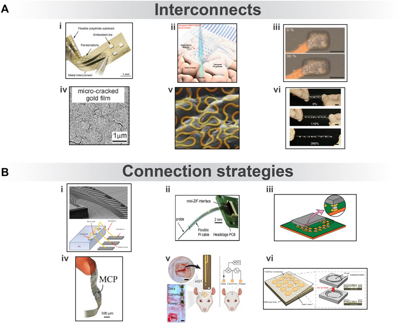
FIGURE 4. (A) Interconnections used to carry electrode information. i) Flexible polyimide-based device with an SI-based dice connected via sputter-deposited metal interconnects. Reproduced from (Stieglitz et al., 2023), licensed CC-BY-4.0. ii) PEDOT: PSS-EG electrodes and interconnects on PET provide a transparent sensing site for ECoG. Reproduced from (Cho et al., 2022), licensed CC-BY-NC. iii) Stretchable thin film cracked gold interconnects. Reproduced from (Lacour et al., 2006), with permission from AIP Publishing. iv) Au–TiO nanowires on the stretchable PDMS substrate, before and after 30% extension. Reproduced from (Tybrandt et al., 2018), licensed CC-BY-NC-4.0. v) Stretchable gold serpentine shapes over a skin replica material. Reproduced from (Fan et al., 2014), with permission from Springer Nature Limited. vi) Silver flake conductive ink is printed onto the stretchable PDMS substrate and retains conductivity of more than 100 S cm−1 up to 260% stretching. Reproduced from (Matsuhisa et al., 2015), licensed CC-BY-4.0. (B) Strategies to connect ribbon cables with rigid electronics. i) Wire bonding mechanism. Reproduced from (Tsai et al., 2016) with permission from IEEE. ii) The flexible PI cable is interfaced with external instrumentation via a mini ZIF connector. Reproduced from (Ayub et al., 2017), with permission from Springer Science Business Media New York. iii) Conventional flip-chip bonding. Reproduced from (Yokoshima et al., 2009), with permission from IEEE. iv) Two conformable arrays bonded by MCP. Reproduced from (Jastrzebska-Perfect et al., 2020b), licensed CC-BY-4.0. v) Conformable VIGT-based neural shank with a power generator and data receiver electrodes placed on the scalp. Reproduced from (Cea et al., 2023), licensed CC-BY-4.0. vi) Capillary forces deform the input/output pad to contact the CMOS pixels, upon which van der Waals forces become significant to establish structural and electrical contact. Reproduced from (Zhao et al., 2023), licensed CC BY-NC-4.0.
Flexible substrates lack the ability to withstand significant deformation. Thin-film metal deposits incorrectly can result in breakage during the deformation of the substrate. For this purpose, the use of nanostructures for interconnects allows high conductivity after repeated elongation (Figure 4Aiii) (Tybrandt et al., 2018). Silver nanowires embedded in PDMS maintain stable conductivity (5,285 S cm−1) in a wide range of strains (0%–50%) (Xu and Zhu, 2012). Similarly, gold microcrack interconnects on an elastomer substrate allow stretching to 32% without fatigue (Figure 4Aiv) (Lacour et al., 2006). Printable elastic conductor ink using silver flakes has also shown a high initial conductivity of 738 S cm−1 and a record high conductivity of 100 S cm−1 when stretched to 260% strain (Figure 4Av) (Matsuhisa et al., 2015). The carbon nanotube (CNT) interconnects on PDMS provides a stretchable transparent electrode array for applications requiring optical transparency (Zhang et al., 2018). Alternatively, the design of cables also enables stretchability materials, and the serpentine layout for interconnects offers exceptional stretchability (50%–90%) (Figure 4Avi) (Zhang et al., 2013). Another study showed that applying multiple cycles of strain (>140%) on the 7-µm Ecoflex substrate caused microcracks in the serpentine interconnects (Pan et al., 2017; Ji et al., 2020). Other layouts like Y-shaped PI/Pt/PI conductive tracks embedded in PDMS demonstrate excellent deformability and electrical stability at the 80% applied strain (Vachicouras et al., 2019). Apart from the metal interconnect, PEDOT: PSS films are both highly conductive and stretchable (higher than 4,100 S cm−1 under 100% strain), giving rise to transistor arrays up to five times higher in the island-to-interconnect ratio as compared to those using wavy metal interconnects (Figure 4Aii) (Qi et al., 2017).
Connectors form the bridge to transfer neural information from interconnects to the back end. However, their assembly with interconnects involves cumbersome probe guiding, wire bonding, and bundling techniques Figure 4Bi (Du et al., 2011). An alternative to wire bonding is solder ball bonding. This process is heat-activated, time-consuming, and requires a large area for cables (Kisban et al., 2007). Hard substrates like thin silicon enable the direct integration of multiplexing circuitry and electrode array on the same substrate, as in the case of Neuropixels (Neuropixels, 2023). However, this limits the flexibility of the probe. Currently, clinically adopted connector technologies allow 200 electrode channels to be connected to one Neuroport connector (Xie et al., 2014). Soft substrates show limited compatibility with these techniques, especially with the reduced contact pad size. Another way to connect flexible ribbon cables to PCBs is through ZIF connectors (Figure 4Bii). Thin ribbon cables require an additional backplate or stiffener around the connection point with a ZIF connector for greater thickness (Gutierrez et al., 2011). To avoid the time-consuming post-fabrication bonding of interconnects, a neural probe is designed with monolithically integrated PI cables and open-ended connectors to accommodate commercial ZIF connectors [(Novais et al., 2021)]. Bumps made on the surface of the film also facilitate a reliable connection such as in the case of flip-chip bonding (Figure 4Biii) (Govaerts et al., 2008). Ball bonding chips from Intan can be placed over a contact pad array of the probe and reflowed in an oven to robustly connect the chip [(intantech, 2023)]. However, due to the limitation of soft substrates to withstand high temperatures, adhesives such as anisotropic tape and paste are used to connect flexible cables with ease (Kim et al., 2010; Kim et al., 2013). Recently, organic mixed-conducting particulate composite materials (MCPs) comprising chitosan and sugar alcohol have been introduced to facilitate the bonding between soft and rigid electronics (Figure 4Biv). MCP creates an anisotropic interface for high-spatiotemporal resolution EEG signals (Jastrzebska-Perfect et al., 2020a). Ultrathin magnetically connectable films also enable freestanding devices that are easily incorporated with magnetic connectors (Zhang et al., 2021; Spanu et al., 2022). Moreover, thick permanent magnets integrated into MEMS systems hold potential for magnetic docking (Zmood et al., 2001; Jackson et al., 2016). Ionic communication is another interesting approach that enables standalone devices with wireless power and data transmission (Figure 4Bv) (Zhao et al., 2022; Cea et al., 2023). Ultimately, capillary and van der Waals forces establish a self-assembled ohmic contact between the electrode pads and CMOS chips (Figure 4Bvi). This is a scalable process that can form thousands of high-density interconnections (Zhao et al., 2023).
Bidirectional neural interfaces can potentially transform the fields of neuroprosthetics, brain–machine interfaces, and neuroscience by enabling bidirectional communication between the brain and external devices. These interfaces can highly impact the area of neuroprosthetics, such as visual prosthesis for the blind (Najarpour Foroushani et al., 2018; Fernández et al., 2020), brain–computer interfaces (BCIs) for individuals with severe disabilities (Even-Chen et al., 2020; Bouton, 2018), and neuroscience by augmenting the neuroscientific toolbox toward the understanding of brain function and the mechanisms underlying various neurological disorders (Müller et al., 2015; Abbott et al., 2019; Shekar et al., 2019).
As the needs of different applications for bidirectional neural interfaces continue to evolve, the technological challenges of these interfaces demand novel tailored solutions. On one hand, neuroprosthetic devices such as visual prostheses for the blind mainly focus on electrical stimulation of hundreds to thousands of sites, where recording is performed only for calibration purposes (Chen et al., 1979; Fernández et al., 2020). On the other hand, BCIs are focused on recording high spatial density and high-fidelity neural activity, where stimulation is performed on a limited number of channels (Ranjandish et al., 2018a; Even-Chen et al., 2020). Finally, some bidirectional neuro-electronic devices would benefit from both high-density recording and stimulation for closed-loop applications (Zhou et al., 2018; Shin et al., 2022; Topalovic et al., 2023). The balance in the directionality of the device shifts the challenges and requirements. For example, in recording-oriented applications, the signal-to-noise ratio, number of recording channels, and up-link data rate constitute the main trade-offs, while in stimulation-oriented applications, power management, power-efficient stimulation, and down-link communication should be optimized. Achieving the best possible trade-offs between these system-level aspects shapes the recent developments in bidirectional neural interfaces (Xu et al., 2019; Liu et al., 2020).
A bidirectional neural interface typically consists of four main blocks, as shown in Figure 5: an analog front end (AFE), which is responsible for amplifying, filtering, and digitizing neural signals from the brain; a stimulation unit, which is responsible for delivering electrical or optical stimulation to the brain to elicit neural activity; a power management unit (PMU), which is responsible for managing the power supply to the other units in the interface and may also include energy harvesting or wireless charging capabilities; and finally, a control unit (CU), which is responsible for processing and analyzing the neural signals and stimulation commands and communicating with external devices such as computers or prosthetic limbs, either using tethered approaches or wireless communications. In the following sections, the state-of-the-art and design decisions of each block will be discussed.
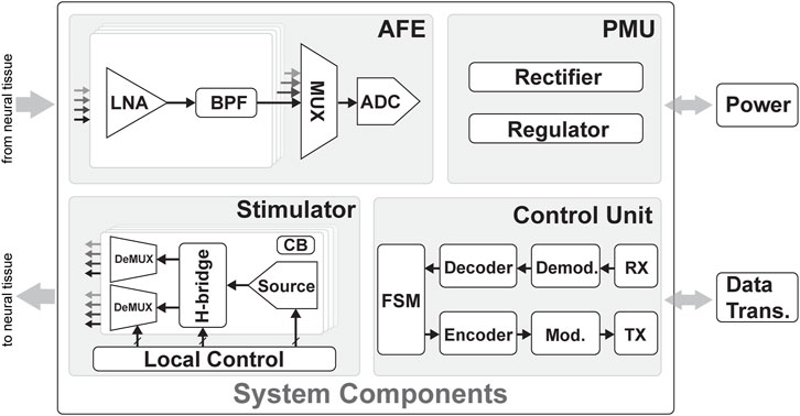
FIGURE 5. Overview of the system components of a bidirectional system with four main components: the power management unit (PMU), control unit (CU), analog front end (AFE), and stimulator unit. The PMU connects to the energy source and regulates the signal to the right voltage supply for the rest of the system. The CU connects to the data telemetry and contains blocks to demodulate incoming data and modulate outgoing data. The AFE contains a low-noise Amplifier (LNA) and bandpass filters (BPFs) and an analog-to-digital converter (ADC) to sense and digitize the neuronal signals from the electrodes. Multiplexers (MUXs) can be used to group several units into a single ADC. The stimulator unit contains the stimulation sources and H-bridges to generate biphasic current pulses; these pulses are demultiplexed (DEMUX) to connect one source to several electrodes. Finally, charge balancing (CB) circuits ensure the long-term safety of the stimulation.
Each of these blocks plays an essential role in the bidirectional flow of information between the brain and external devices and must be carefully designed and optimized for optimal performance and safety. The main trade-offs for the AFE and stimulation unit are area, power, safety, and reconfigurability. The focus of a device weighs the trade-offs in different scenarios. For example, a device developed for research purposes will likely benefit from high reconfigurability to gather all data, and the area or power is not limiting. At the same time, a system that needs to be implanted has strict requirements on the area and power consumption, which can be improved by compromising the reconfigurability of the device. In addition, challenges in implementing wireless power and communication include optimizing the power transfer efficiency, ensuring biocompatibility and stability, maintaining data security, and obtaining regulatory approval. Addressing these challenges is crucial to advance wireless power and data transmission in implantable neural interfaces and improving healthcare for individuals with neurological disorders.
Wireless communication and power transfer of medical devices are limited to the industrial, scientific, and medical (ISM) frequency bands. Popular center frequencies are 6.78, 13.56, and 40.68 MHz. Higher frequencies lead to higher absorption in the tissue (Gabriel et al., 1996), which is limited by a specific absorption rate (SAR) but leads to higher data rates and requires smaller transmitter components. Wireless power transmission in implantable neural interfaces at short implantation depths primarily utilizes inductive coupling (Kiani, 2022), which transfers power through electromagnetic fields. It involves an external power transmitter generating a magnetic field to induce a current in a receiving coil within the implant. Another method, radio frequency (RF) energy harvesting (Lee et al., 2020b), captures ambient electromagnetic radiation using antennas to convert it into electrical energy. Other methods for power transmission include ultrasound (Seo et al., 2016; Shi et al., 2021), NFC (He et al., 2018a), and infrared-based (IR) methods (Moon et al., 2021) Wireless data transmission methods include RF communication using electromagnetic waves (Lee and Ghovanloo, 2011), Bluetooth (Hampson et al., 2009; Zhou et al., 2018; Idogawa et al., 2021; Lee et al., 2023), near-field communication (He et al., 2018b), and optical communication with IR (Moon et al., 2021) or visible light (Xu et al., 2023).
The Analog front end (AFE) is one of the important units of a bidirectional neural interface. Its main purpose is to record, amplify, filter, and convert analog signals to digital signals. This recording unit is a crucial tool in various fields, including neuroscience research (Zhou et al., 2018), neuroprosthetics (Lo et al., 2017), neurological disorders (Lo et al., 2017; Ranjandish et al., 2018a; Rozgic et al., 2019; Jia et al., 2020; Uehlin et al., 2020), and clinical applications (Sahasrabuddhe et al., 2020). They enable scientists and clinicians to gain insights into neural functioning, study brain disorders, develop therapeutic interventions, and potentially restore lost sensory or motor function. In the following paragraphs, we will discuss the different blocks of an AFE and the most important challenges of each part.
The primary goal of an LNA is to amplify the weak neural signals while introducing as little additional noise as possible. Since neural signals are typically very small, on the order of micro-volts (µV), and are easily contaminated by various sources of electrical noise, we use the LNA before converting the analog signal to digital using an ADC. The most critical aspect of an LNA is its noise performance. It should have an extremely low input-referred noise level to avoid masking or distorting the neural signals of interest. In addition to noise performance, the LNA should provide a controllable and stable amplification gain. The gain should be sufficient to bring the weak neural signals to a measurable range without saturating or distorting the output. It is important to balance the gain with noise performance to achieve optimal results. Furthermore, the amplifier’s bandwidth determines the range of frequencies it can effectively amplify. It should cover the frequency range of the neural signals to avoid attenuating or distorting them. The bandwidth should be wide enough to capture both low-frequency and high-frequency components of the neural activity. Having an AFE with programmable gain and bandwidth (Ranjandish et al., 2018a) is desirable because it gives us reconfigurability in applications where the signal levels can vary significantly or the signal contains a wide range of frequencies; in these cases, focus on one part only might be required. Moreover, the amplifier should exhibit stable and linear characteristics over its intended operating range. Stability ensures that the gain and noise performance remains consistent over time, while linearity preserves the fidelity of the amplified signals. In terms of the input impedance of the amplifier, it should be high to minimize signal loading and avoid altering the neural signals. High input impedance ensures that the amplifier does not draw significant current from the neural tissue, preserving the integrity of the signals. Moreover, neural recording interfaces are often used in implantable or portable devices, so power consumption is an important consideration. The LNA should be designed to consume minimal power while maintaining its performance specifications. In addition, the neural recording interface needs to be miniaturized and integrated with other components in many cases. The LNA should be designed with compactness and integration in mind, allowing for efficient integration into the overall system. To this end, nowadays, most of the state-of-the-art neural recording systems are designed with CMOS technology as a system-on-a-chip (SoC) that contains all different units of neural recording systems as well as the AFE, which contains the LNA (Lo et al., 2017; Ranjandish et al., 2018a; Jia et al., 2020; Uehlin et al., 2020; Shin et al., 2023).
Designing an ultra-low noise amplifier for neural recording interfaces requires careful consideration of these specifications to ensure optimal performance and accurate neural signal acquisition. It often involves a trade-off between different parameters, such as gain, noise, and power consumption, to strike the right balance for the specific application.
DC drift cancellation is a technique used in AFEs to remove or mitigate the effects of a DC offset or drift in recorded neural signals. A DC offset refers to a constant voltage offset that may be present in the recorded signal. In contrast, a DC drift refers to slow variations or fluctuations in the baseline voltage level over time. These DC components can obscure the neural signals of interest and make accurate signal analysis challenging. There are different methods to eliminate a DC drift. One common approach to removing a DC offset is AC coupling (Harrison et al., 2007; Jia et al., 2020; Sahasrabuddhe et al., 2020; Lee et al., 2023). AC coupling involves inserting a high-pass filter in the signal path, which attenuates low-frequency components, including the DC offset. AC coupling is often achieved using a series capacitor in the signal path. In cases where AC coupling alone is insufficient or when dealing with a DC drift, additional techniques are applied to estimate and remove the DC component. This involves continuously monitoring and estimating the DC offset or drift value (Uehlin et al., 2020; Shin et al., 2023). This estimation can be achieved using various methods, such as averaging or adaptive algorithms. Once the DC offset or drift is estimated, it can be subtracted from the recorded signal to eliminate its influence. Another way is to incorporate calibration procedures to determine and compensate for the DC offset or drift. Calibration involves acquiring reference signals with known characteristics and using them to estimate and adjust the system’s DC offset or drift. This calibration process can be performed periodically or whenever necessary to maintain accurate signal acquisition (De Dorigo et al., 2018). Another approach to mitigate a DC drift is through differential amplification (Ghanbari et al., 2019). The common-mode DC offset or drift can be canceled by using differential amplifiers, which amplify the voltage difference between two input signals rather than a single-ended signal. Differential amplification helps reject common-mode signals, such as the DC offset or drift while preserving the differential neural signals. Sometimes AC-coupling is used with differential amplification (Wang et al., 2019).
It is important to note that DC drift cancellation techniques are typically employed in the analog domain before digitizing the signal for further processing. The specifics of DC drift cancellation methods may vary depending on the design and requirements of the neural recording system, including the number of channels, desired signal quality, and power constraints. By effectively canceling or mitigating DC offset and drift, neural recording systems can ensure accurate acquisition and analysis of neural signals, enabling researchers to study and understand the underlying neural activity more effectively.
Analog-to-digital converters (ADCs) are essential components in an AFE, and their selection and implementation are critical for accurate and reliable signal acquisition. Specifics such as resolution, sampling rate, and the ADC topology can have a significant impact on the performance and power consumption of the ADC. Reducing power and area in ADCs can be achieved using low-power topologies, multichannel ADCs, advanced process technology, and calibration techniques. Multiplexing one ADC over multiple channels is common in neural recording systems to achieve power and area savings. The choice of ADC topology for a neural recording interface depends on various factors such as power consumption, resolution, speed, linearity, noise performance, and area constraints. Different ADC topologies have different trade-offs and are suitable for different applications. Successive approximation register (SAR) ADC is a popular choice for low-to-medium resolution applications, typically ranging from 8 to 16 bits (Wang et al., 2019; Jia et al., 2020; Uehlin et al., 2020; Shin et al., 2023). It operates by iteratively comparing the input voltage with a reference voltage using a binary search algorithm. SAR ADCs offer a good resolution, low power consumption, and relatively low area requirements. However, they may have limited speed compared to other topologies, and the conversion time increases with higher resolution. In addition, delta-sigma ADCs are widely used in applications where high resolution (often 16–24 bits) and high accuracy are required (De Dorigo et al., 2018). They utilize oversampling and noise-shaping techniques to achieve excellent linearity and noise performance. Delta-sigma ADCs are known for their superior performance in low-frequency applications and their ability to suppress noise. However, they typically have slower conversion rates and higher power consumption than other topologies.
The selection of the best ADC topology for a neural recording interface should consider the application’s specific requirements. If high resolution is crucial, a delta-sigma ADC may be preferred. A SAR ADC can be a suitable choice for lower-resolution and power-constrained applications. A pipeline ADC could be a good option if high-speed acquisition is the priority. Additionally, noise performance, power consumption, and area requirements should be carefully evaluated to ensure the chosen topology meets the desired specifications of the neural recording interface.
On-chip signal processing is the technique of performing signal processing functions directly on the integrated circuit (IC) of a neural recording interface. It involves implementing signal processing algorithms, such as filtering, amplification, and feature extraction, in hardware, software, or a combination of both, on the same chip as the neural recording front-end. One of the advantages of using on-chip signal processing is reducing data bandwidth requirements by extracting relevant features of the recorded neural signals, allowing for efficient data storage and transmission. Furthermore, it enables real-time feedback and control, allowing for closed-loop experiments and neural prosthetic applications. Moreover, it improves the signal-to-noise ratio and dynamic range by removing unwanted noise and amplifying the neural signals. In addition to all other advantages, on-chip signal processing enables power-efficient processing by reducing the amount of data transmitted off-chip and minimizing external processing requirements. However, on-chip signal processing increases the chip area and power consumption due to the additional signal processing circuitry. It may also introduce extra noise and distortion due to the processing algorithms or hardware implementation limitations. Finally, using on-chip signal processing requires careful optimization of the algorithms and hardware to balance the trade-offs between processing complexity, power consumption, and area requirements.
Typically, there are three on-chip signal processing approaches. Digital signal processing (DSP) involves implementing signal processing algorithms using digital logic circuitry (Shin et al., 2023). This method offers flexibility in the design of the algorithms and can provide high precision and accuracy. However, implementing the digital logic requires additional power and area, which can be a limitation in low-power applications. Moreover, analog signal processing (ASP) involves performing signal processing functions using analog circuitry (Lee et al., 2023). This method can provide low power consumption and fast processing speeds, but it can be challenging to achieve high accuracy and precision due to the limitations of analog circuitry. In addition, there is mixed-signal processing (MSP) (Shin et al., 2022). MSP combines digital and analog signal processing techniques to balance accuracy, power consumption, and area requirements. This method offers the benefits of both digital and analog processing and is commonly used in neural recording interfaces.
Multiplexing is a technique used in neural recording devices to reduce power consumption and save area by sharing resources among multiple channels. In neural recording, multiplexing refers to sequentially or simultaneously acquiring signals from multiple electrodes or channels using a shared set of components. By multiplexing multiple channels onto a shared set of components, the overall power consumption and circuit area can be significantly reduced compared to having dedicated components for each channel.
Time-division multiplexing (TDM) is a common multiplexing technique used in neural recording devices (Berényi et al., 2014; Wang et al., 2019; Uehlin et al., 2020). It involves sequentially sampling the signals from each channel during different time slots. Sharing a single ADC across multiple channels can prevent the power consumption associated with multiple ADCs. TDM also reduces the required interconnects since the channels are time-multiplexed onto a single data line. Frequency division multiplexing (FDM) is another technique where different channels are assigned distinct frequency bands (Mikawa et al., 2019; Kim et al., 2021). Each channel’s signal is modulated onto a unique carrier frequency and combined into a single composite signal. FDM enables the simultaneous acquisition of multiple channels, reducing the overall acquisition time and allowing the efficient use of shared components.
Multiplexing techniques can be implemented in different locations of the AFE scheme. The simplest way is as shown in Figure 6A, with no multiplexing in AFE and just multiplexing all the data from AFE to other units. One of the most popular methods is to share one ADC among M channels Figure 6B. This can reduce the area and power consumption of the IC. However, the sampling frequency of the ADC increases M times, which can increase the power consumption of the ADC, and even driving buffers would be needed in the input of the ADC (Hashemi Noshahr et al., 2020). A new approach is to use multiplexing at the input of a single AFE shared by all channels (Figure 6C). This reduces space per channel and eliminates mismatches between channels, potentially lowering power consumption compared to traditional setups. However, this approach requires a high-bandwidth LNA to quickly multiplex all channels, which increases power consumption and introduces in-band noise due to aliasing (Sharma et al., 2018). Another technique for increasing the number of electrodes is to use a switch array. In this method, out of an array of M electrodes, N are selected and connected to AFEs Figure 6D (Dutta et al., 2019). The specific multiplexing scheme depends on the system requirements, the number of channels, and the desired trade-offs between power consumption, area utilization, and signal quality.
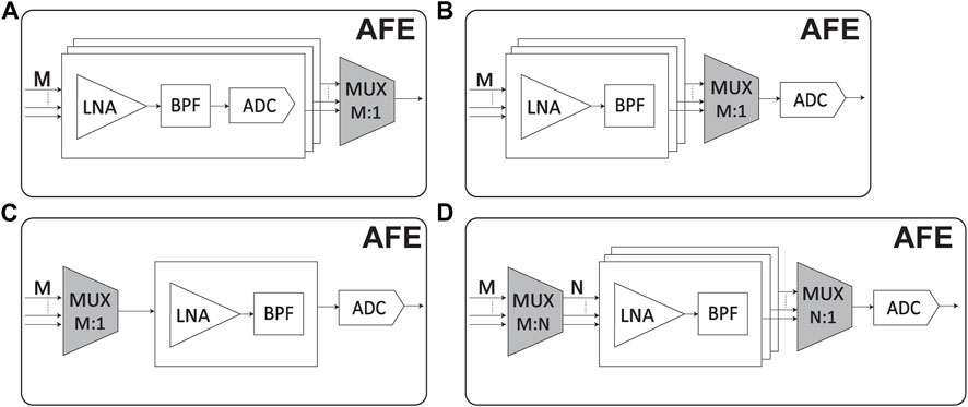
FIGURE 6. Block diagram of different AFEs based on the location of the multiplexer. (A) Non-multiplexing, (B) sharing ADC between M channels, (C) sharing AFE between M channels, and (D) switch array multiplexing (sharing N AFEs with M electrodes and one ADC for all N AFEs).
In electrical stimulation, electrical pulses are applied to the electrodes to activate nearby neurons. The pulses can be current- or voltage-driven, but current-mode stimulation (CMS) is commonly used as it offers better control over the charge delivery, which improves the safety of the stimulation. Conventionally, rectangular pulses are used for ease of implementation. The stimulation phase is followed by a balancing phase with opposite polarity to restore the charges delivered in the first phase, resulting in biphasic stimulation pulses. An example of a biphasic current pulse and resulting voltage transients are shown in Figure 7A. In some cases, other pulse shapes, such as Gaussian or triangular, are used with the aim to improve the energy efficiency of the stimulation (Wongsarnpigoon and Grill, 2010; Foutz et al., 2012). However, in this regard, it is important to consider additional losses that might occur in the output driver due to the non-rectangular pulse shapes as it might negate the efficiency improvement (Varkevisser et al., 2022).
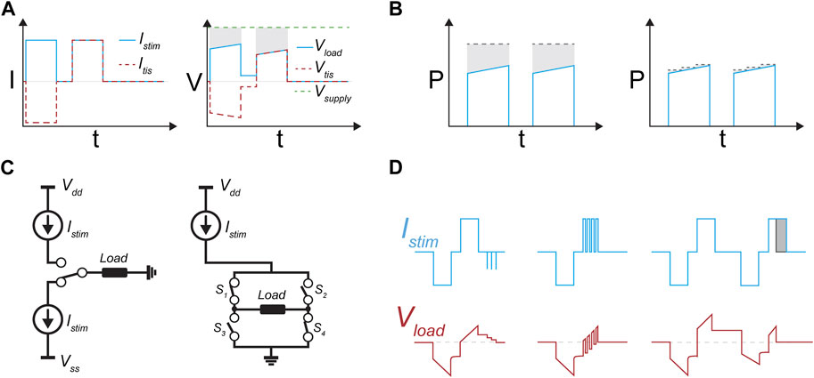
FIGURE 7. (A) Typical biphasic current pulse used in current-mode stimulation (left) and resulting voltage over the electrodes. (B) Power overhead losses when using a fixed voltage supply (left) and power saving opportunity of voltage scaling (right). (C) Monopolar (left) and bipolar (right) electrode configurations used in current-mode stimulators. (D) Examples of active charge-balancing techniques: pulse insertion (left), chopped anodic phase (middle), and anodic phase adjustments (right).
The essential blocks in a neurostimulator circuit are the stimulation source and a switch configuration to direct the stimulation toward the electrodes. Additional circuits can be added for safety or efficiency improvements. Multichannel stimulation systems often implement a modular architecture (Mikawa et al., 2019; Reich et al., 2021; Noorsal et al., 2022), offering several advantages of power, area, and complexity (Mikawa et al., 2019). In a modular architecture, the system is divided into multiple stimulation modules, each containing the essential components for a stimulation channel. Moreover, in stimulation, multiplexing can be used to save area. Using temporal interleaving, one stimulation source can drive multiple channels in one period (Kameda et al., 2014). However, this limits the reconfigurability of the stimulator as it requires a specific temporal pattern for multichannel capabilities. Depending on the application, spatial interleaving can also be applied. If not, all channels need to be stimulated in a single period and the module can connect to more electrodes than fit into one period. This reduces the size of the total system even further. However, the switch matrix that connects the source to each electrode increases in complexity.
Different electrode configurations can be used, as shown in Figure 7C. In a monopolar configuration, the stimulation electrode is driven both positively and negatively with respect to a distant reference electrode to create a biphasic pulse. This configuration thus requires two separate current sources. A bipolar configuration uses two nearby electrodes to deliver the stimulation. In this configuration, it is possible to use two current sources or a single source and change the connection to the electrodes to create biphasic pulses. Lastly, multipolar configurations are similar to the bipolar configuration, but multiple activation and/or return electrodes can be used.
Even though CMS is preferred for its charge controllability, the voltage drop over the current source leads to additional power dissipation, indicated by the shaded area in Figure 7A. Particularly in multichannel configurations, this leads to degradation of the power efficiency. In a multichannel system, the voltage supply must accommodate the channel with the highest voltage requirement. All other channels suffer from excessive losses in the current source. A scalable voltage supply can be used to reduce the overhead losses, as illustrated in Figure 7B. Different voltage scaling architectures have been proposed. Some designs control the output voltage from the transmitted power to the device (Noorsal et al., 2022). However, this regulation only allows adaptation of the system-level voltage supply. Thus, the efficiency improvement in a multichannel system is limited because it cannot regulate individual channels. Alternatively, on-chip DC/DC converters are used to scale the voltage supply (Arfin and Sarpeshkar, 2012; Luo et al., 2017; Luo and Ker, 2018). Depending on the implementation of the converter, this method can be suitable for multichannel systems. The area required for the converter, commonly implemented as a switched-capacitor DC/DC converter (Luo et al., 2017; Luo and Ker, 2018), is a limiting factor for channel-specific regulation. To overcome this problem, a multi-output DC/DC converter can be used (Rashidi et al., 2016). In this way, one converter can regulate multiple channels individually. As will be discussed in Section 4.3, adaptive voltage regulation is often integrated with the rectifier circuit to overcome conversion losses that lead to cascaded inefficiencies. In a modular system, a separate, scalable voltage supply for each module would lead to the best power performance. However, implementing a scaled voltage supply can be costly in the area. Therefore, the appropriate trade-off between area and power efficiency should be made.
The secondary phase of the biphasic current pulses restores the applied charge of the first phase because charge accumulation on the electrode interface can lead to harmful electrochemical reactions (Merrill et al., 2005). However, mismatches in the charge of both phases can still lead to accumulation over multiple periods. Charge balancing (CB) measures are required to prevent this and ensure long-term safety. The simplest implementation of charge balancing is passive discharge. After a stimulation pulse, the electrodes are connected, and any residual charge can discharge. The speed of this process is dependent on the impedance of the electrodes, and for many applications, the discharge rate is not fast enough to ensure safety in the long term (Sooksood et al., 2009). For faster recovery of residual charge, active CB techniques should be used. Active CB requires monitoring the residual charge, which can be performed by measuring the voltage over the electrodes when no current is present. Following this measurement, several methods can reduce the residual charge. The pulse insertion technique (Ortmanns et al., 2007; Sooksood et al., 2009; Jia et al., 2020; Pu et al., 2022) alternates current pulses with voltage measurement until the charge balance is satisfied. Instead of inserting pulses afterward, a chopped second (anodic) phase can directly control the charge to equilibrium (Ranjandish and Schmid, 2016; Ranjandish et al., 2018b). Alternatively, the anodic phase of subsequent pulses can be adjusted (Rathna, 2016; Son and Cha, 2020; Eshaghi et al., 2021). This requires several periods to restore CB but only one voltage measurement per period and thus reduces the time of a single period compared to the other techniques. The signal diagrams of some common CB techniques are shown in Figure 7D.
Table 1 compares several important parameters in designing a bidirectional neural interface, which concludes both recording and stimulation circuits. Artifact suppression, SoC integration, and on-chip processing are the focus of these works. Improving these techniques will make it possible to increase the number of recording and stimulation channels. Table 1 shows that having a high number of channels for both recording and stimulation is still a challenge, and more studies should be conducted in this regard. As for the recording units, the bandwidth of each design is different, depending on the target signal. The bandwidth for local field potentials (LFPs) is mostly around 200 Hz, while for spikes and action potentials, it is between 200 Hz and 10 kHz.
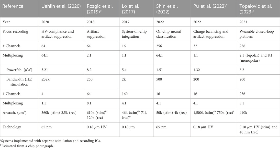
TABLE 1. Comparison of state-of-the-art bidirectional neural interface designs.
Wireless power transfer can be achieved by many modalities, such as inductive, ultrasound, or capacitive links (Kiani, 2022). Inductive links are widely preferred for biomedical implants where the wireless power transfer occurs over a short distance (near-field) between the transmitting and receiving devices (Noorsal et al., 2012; Rozgic et al., 2019; Jia et al., 2020; Kiani, 2022). An inductive power link uses resonance circuits to improve the coupling and power transfer. The resonating tank consists of a series or parallel-connected inductance and capacitor (LC) couple. For biomedical implants’ power and distance ranges, a parallel configuration on the receiver side is usually preferred (Jay and Palermo, 2014; Lukatskaya, 2016).
The power-receiving module has two main functions: rectifying the incoming signal and regulating the required voltage levels. The voltage conversion efficiency (VCR), the ratio between the output voltage and the peak voltage of the input signal, and power conversion efficiency (PCE), the ratio between the power delivered to the load and the received power, are two important metrics to compare the performance of power management stages. The simplest implementation of a rectifier circuit only uses diodes or diode-connected MOSFETs. However, these passive rectifiers suffer from a voltage drop over the diodes, which limits the VCR. The voltage drop over the diodes also causes conduction losses, leading to a reduced PCE. To overcome these drawbacks, active rectifier structures are proposed. In an active rectifier, diode-connected MOSFETs on one side (NMOS/PMOS) are replaced with actively controlled MOSFETs, and the other side is implemented with cross-coupled MOSFETs, as shown in Figure 8A. The active feedback circuit lowers the voltage drop over the MOSFETs, reducing the conduction losses and improving the VCR. However, the non-ideal timing of the switching leads to a reduction of the received power and possible reverse currents, degrading the performance of the rectifier (Lukatskaya, 2016). To prevent this, compensation techniques are proposed to minimize the delays in switching. The compensation circuits focus on compensating the delay of the feedback circuit by introducing an offset to the decision comparator (Lee and Ghovanloo, 2013; Li et al., 2015a; Lukatskaya, 2016; Hu et al., 2018; Ozalevli et al., 2018; Pal and Ki, 2020; Van Mulders et al., 2022).
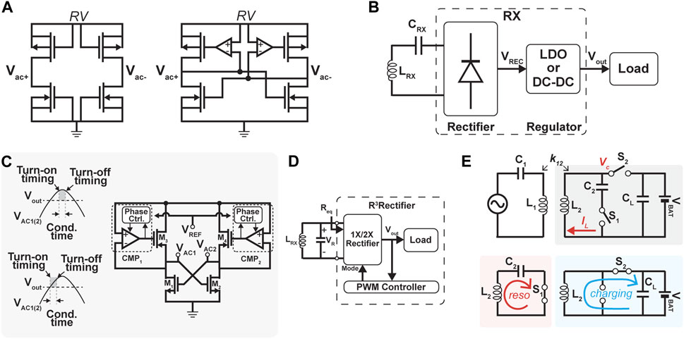
FIGURE 8. (A) Passive (left) and active (right) rectifier topologies [reproduced from (Almarri et al., 2023), licensed CC-BY-4.0]. (B) Conventional two-stage power management strategy using a rectifier, followed using a voltage regulator [reproduced from (Liu et al., 2018), licensed CC-BY-4.0]. (C) Regulating rectifier using phase control [adapted from (Liu et al., 2018), licensed CC-BY-4.0]. (D) Reconfigurable regulating rectifier (3R) [adapted from (Liu et al., 2018), licensed CC-BY-4.0]. (E) Multicycle current-mode regulation [adapted from (Kim et al., 2022), with permission from Korean Society of Medical and Biological Engineering].
The conventional architecture of a power management unit (PMU) in wirelessly powered systems consists of the receiving elements and a rectifier circuit that converts the incoming AC signal to a DC voltage, followed by a regulating stage that regulates the rectified voltage to a stable voltage required by the system, as shown in Figure 8B. However, the inefficiencies of both stages are cascaded, leading to low overall efficiency of the PMU. To improve efficiency, single-stage rectifying regulator circuits have been introduced. One method of regulating the output of an active rectifier is by controlling the conduction time of the active diodes (Figure 8C) (Liu et al., 2018). The design in (268) implements a phase control in the decision comparator to regulate the output voltage. Similarly, Kim et al. (2017) used pulse-width modulation (PWM) to control the conduction time of the switches and regulate the output voltage. However, for light loads, the conduction time would be short, leading to low PCE due to switching losses. Therefore, pulse frequency modulation (PFM) was added to reduce the switching events and increase the conduction time for low-power loads. Another method of single-stage regulation is a reconfigurable regulating rectifier topology (Figure 8D) (Li et al., 2015a; Li et al., 2015b; Cheng et al., 2017; Lu et al., 2023). The rectifier can switch between different gain (e.g., 1x and 2x) configurations in these designs. Additionally, using PWM control between different configurations, intermediate output voltages can be achieved. Finally, a multicycle regulation method can be used (Figure 8E) (Gougheri and Kiani, 2016; Lee et al., 2016; Lee HS. et al., 2022; Kim et al., 2022). This method uses the LC tank in two modes: resonant and charging modes. In the resonant mode, the tank is parallel connected and disconnected from the circuit for multiple cycles. This causes an energy build-up in the LC components. In the charging mode, the inductor is series connected to the storage capacitor, causing it to charge. In this way, the output voltage can be boosted above the incoming peak voltage without the need for bulky components of DC/DC boost topologies (Liu et al., 2018).
Wireless data transmission in neural interfaces utilizes various approaches to establish communication between the brain and external devices. Radiofrequency (RF) signals can be used to wirelessly transmit data between the neural interface and an external device (Jia et al., 2020). This method utilizes electromagnetic waves in the radio frequency range to carry information. RF communication is a commonly used wireless technology with well-established standards, making it widely accessible. RF signals can be transmitted over longer distances, allowing for more flexibility in device placement, and RF communication can achieve high data transfer rates, enabling real-time transmission of neural data. However, RF signals can be susceptible to interference from other electronic devices, potentially leading to data corruption or loss. In addition, RF communication often requires more power, which can impact the neural interface’s size, weight, and battery life. Moreover, RF signals can be intercepted, raising security concerns. Encryption and authentication measures should be implemented to mitigate risks.
Another approach for wireless data transmission is using Bluetooth (Hampson et al., 2009; Zhou et al., 2018; Idogawa et al., 2021; Lee et al., 2023). Bluetooth technology enables short-range wireless communication between devices. It can be utilized to establish a wireless link between the neural interface and a computer or mobile device. In addition, Bluetooth is supported by various devices, making it easier to connect with different platforms. Moreover, Bluetooth offers simple pairing and automatic connection capabilities, enhancing user convenience. On the other hand, Bluetooth has a relatively short-range communication capability, which may restrict the distance between the neural interface and the external device, and it consumes more power compared to other modalities, which can reduce the battery life. In addition, Bluetooth connections may have limited bandwidth, affecting the real-time transmission of large amounts of neural data. Furthermore, Bluetooth signals can experience interference from other devices operating in the same frequency range.
Using NFC is another method of wireless communication (He et al., 2018b). NFC allows for communication by bringing devices into close proximity, making it user-friendly and easy to initiate. NFC is designed for low-power applications, contributing to efficient energy usage in the neural interface. NFC utilizes encryption and authentication protocols, enhancing security during data transmission. Nevertheless, NFC has a short-range communication distance, typically within a few centimeters, which restricts the physical proximity between devices. Furthermore, NFC offers lower data transfer rates than other wireless technologies, limiting the amount of data that can be transmitted simultaneously. In addition, NFC requires devices to have NFC capabilities, which may not be universally available across all platforms.
Another method for data communication is using ultrasound (US) (Shi C. et al., 2020). US communication involves the transmission and reception of data using ultrasound waves with frequencies above the upper limit of human hearing (typically above 20 kHz, in the range of MHz). US offers centimeters of penetration due to its low tissue attenuation (Culjat et al., 2010). In addition, a much higher safe exposure intensity limit is allowed in ultrasound compared to RF (FDA, 2023). In addition to these modalities, using infrared (IR) light waves is another approach to wireless data communication (Moon et al., 2021). IR data communication typically involves two main components, an IR transmitter and an IR receiver. The transmitter emits modulated infrared signals containing the data to be transmitted, while the receiver captures and decodes these signals to retrieve the original data. Optoelectronic device technologies allow for high efficiency at the micrometer scale, which makes IR a good option for sub-micrometer data communications. However, IR data communications require a clear line of sight between the transmitter and receiver, meaning obstacles can interfere with the signal. In addition, IR signals have relatively short-range capabilities (<1 mm) compared to other methods (Wu et al., 2018).
There are different configurations for power and data transmission. One approach is to utilize separated inductive links for power and data transmission, as shown in Figure 9A (Ghovanloo and Atluri, 2007; Mandal and Sarpeshkar, 2008). This method allows for independent optimization of each link, resulting in increased data rate (Mandal and Sarpeshkar, 2008) and improved power efficiency. However, it requires a more complex antenna and experiences issues with crosstalk among the links (Ghovanloo and Atluri, 2007). Another configuration is using RF data links for data communication and inductive link for power transmission, as shown in Figure 9B. It can achieve higher data rates, but it consumes significantly more energy and requires more complex circuits and antenna structures. The simplest approach is to use a single inductive link for both power and data transmission (Figure 9C). In this technique, passive backward communication relies on backscattering. However, a limitation of this approach is that the power efficiency and data rate are constrained by conflicting requirements for efficient power transmission and high data rate (Mayordomo et al., 2013). Each approach to wireless data transmission in neural interfaces has its own set of advantages and limitations. The choice of method depends on the application’s specific requirements, including factors such as range, data transfer rates, power consumption, compatibility, and security considerations. Ongoing research and advancements in wireless communication technologies continue to improve the performance and capabilities of wireless neural interfaces.
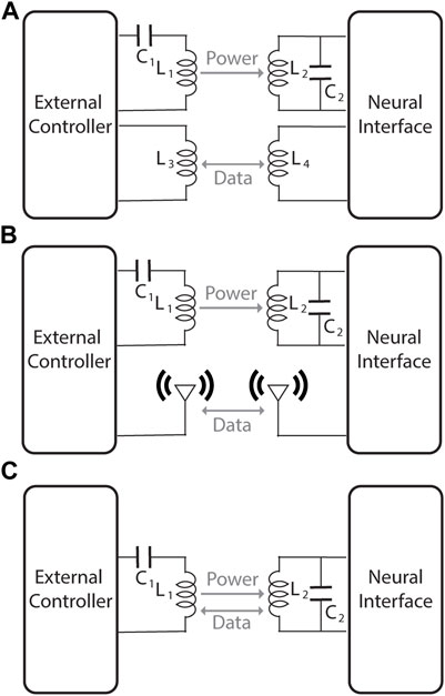
FIGURE 9. Examples of possible power and data transmission configurations. (A) Two separate inductive links are used. (B) An inductive power link is combined with an RF data link. (C) Power and data transmission use the same inductive link. Figure adapted from (Ha et al., 2019), with permission from Elsevier Inc.
The field of biomedical technology is inherently at the interface between various disciplines. Biology, medicine, engineering, and materials science are some of the fields relevant to advancing devices and therapeutics. However, in the fields of materials science and engineering, research, for example, on various technologies and materials branches out and leads development in parallel. Efficient problem-solving capacity necessitates not only collaboration and information exchange across disciplines but also across technology and materials development routes. This becomes obvious when we partition a biomedical device into a minimum number of functional parts or relevant problems that require specific solutions, but less so if we look at one of these parts and the different solutions that may be available, or the communication among them. Inter-technology/material solutions are needed.
To develop a biomedical device, interdisciplinary thinking is inevitable to even ask the right questions. However, some may have multiple answers (or solutions). Should we always choose the best solution that we have at hand? This question highlights the boundaries between research and development, novel and established (Figure 10). Innovation requires the right balance between those and quantized information exchange among different technology and material branches. University researchers have the luxury of not depending on financial outcomes, which enables shorter periods of information exchange and drives innovation. On the other hand, companies choose to either go for the best solution at hand or invest in research, which crosses the new and the established less frequently.
FIGURE 10. Interdisciplinarity and inter-technological solutions as a drive of innovation.
As a more concrete example, in the context of engineering and materials science, which relate to the research and development of hardware for neural interfaces, the combination of organic materials and CMOS circuits has emerged as a promising avenue for advancing the capabilities of BCIs and facilitating seamless communication between the human brain and electronic devices. This convergence of organic and inorganic materials shows potential to bring together the best of both worlds, enabling high-performance neural interfaces with enhanced biocompatibility and functionality. The fields of CMOS neural interfaces and organic bioelectronics have been mostly developing individually; however, there are indications that organic bioelectronics may offer the best front-end properties to the interface with neurons, while CMOS neural interfaces do not have, yet, any rival in terms of processing capabilities. Although curiosity-driven research should be prioritized in these individual fields, such that, on their own, novel improved solutions can be found, it is also clear that synergies between these technologies may lead to new breakthrough discoveries that have not yet been untapped. The combination of organic materials and CMOS circuits in neural interfaces presents, however, unique engineering challenges. The integration process requires careful consideration of material compatibility, electrical interfaces, and manufacturing techniques. Researchers are exploring innovative methods, such as flexible hybrid electronics, where organic and CMOS components are integrated on flexible substrates, enabling conformal and unobtrusive integration with neural tissue, with the organic materials in close contact with tissue and the CMOS components encapsulated with biocompatible materials and further away from the neural tissue of interest.
In conclusion, we hope that this review serves the scientific community by helping researchers to grasp and/or organize information on neural interfaces and that it promotes interdisciplinarity and inter-technology solutions that hold great potential for improving the quality of life for individuals with neurological conditions and ushering in a new era of human–machine interactions.
SD, FV, LS, and MA contributed equally to this work. TLC and GDS supervised this work. All authors contributed to the article and approved the submitted version.
This work was supported by the project G0F9421N, which has received funding within the framework of the Odysseus program from the Research Foundation—Flanders (FWO), as well as the project UPSIDE (ID 101070931), which has received funding within the framework of Horizon EIC 2021 Pathfinder Challenges by European Union. FV was supported by INTENSE project funded by the Dutch Research Council (NWO) under grant number 17619.
The authors declare that the research was conducted in the absence of any commercial or financial relationships that could be construed as a potential conflict of interest.
All claims expressed in this article are solely those of the authors and do not necessarily represent those of their affiliated organizations, or those of the publisher, the editors, and the reviewers. Any product that may be evaluated in this article, or claim that may be made by its manufacturer, is not guaranteed or endorsed by the publisher.
Abbott, J., Ye, T., Krenek, K., Gertner, R. S., Ban, S., Kim, Y., et al. (2019). A nanoelectrode array for obtaining intracellular recordings from thousands of connected neurons. Nat. Biomed. Eng. 4 (2), 232–241. doi:10.1038/s41551-019-0455-7
Abidian, M. R., Corey, J. M., Kipke, D. R., and Martin, D. C. (2010). Conducting-polymer nanotubes improve electrical properties, mechanical adhesion, neural attachment and neurite outgrowth of neural electrodes. Small 6 (3), 421–429. doi:10.1002/smll.200901868
Abidian, M. R., and Martin, D. C. (2009). Multifunctional nanobiomaterials for neural interfaces. Adv. Funct. Mater 19 (4), 573–585. doi:10.1002/adfm.200801473
Airaghi Leccardi, M. J. I., Vagni, P., and Ghezzi, D. (2019). Multilayer 3D electrodes for neural implants. J. Neural Eng. 16 (2), 026013. doi:10.1088/1741-2552/aae191
Alhabeb, M., Maleski, K., Anasori, B., Lelyukh, P., Clark, L., Sin, S., et al. (2017). Guidelines for bynthesis and processing of two-dimensional titanium carbide (Ti 3 C 2 T x MXene). Chem. Mater. 29 (18), 7633–7644. doi:10.1021/acs.chemmater.7b02847
Almarri, N., Jiang, D., Langlois, P. J., Rahal, M., and Demosthenous, A. (2023). High efficiency power management nnit for implantable optical-electrical stimulators. IEEE Open J. Circuits Syst. 4, 3–14. doi:10.1109/ojcas.2023.3240644
Altuna, A., Gabriel, G., De La Prida, L. M., Tijero, M., Guimerá, A., Berganzo, J., et al. (2010). SU-8-based microneedles for in vitro neural applications. J. Micromechanics Microengineering 20 (6), 064014. doi:10.1088/0960-1317/20/6/064014
Amar, A., Kouki, A., and Cao, H. (2015). Power approaches for implantable medical devices. Sensors 15 (11), 28889–28914. doi:10.3390/s151128889
Ansaldo, A., Castagnola, E., Maggiolini, E., Fadiga, L., and Ricci, D. (2011). Superior electrochemical performance of carbon nanotubes directly grown on sharp microelectrodes. ACS Nano 5 (3), 2206–2214. doi:10.1021/nn103445d
Aquilina, O. (2023). A brief history of cardiac pacing. Available from: https://www.ncbi.nlm.nih.gov/pmc/articles/PMC3232561/.
Araki, T., Bongartz, L. M., Kaiju, T., Takemoto, A., Tsuruta, S., Uemura, T., et al. (2020). Flexible neural interfaces for brain implants-The pursuit of thinness and high density. Flexible Print. Electron. 5, 043002. doi:10.1088/2058-8585/abc3ca
Arfin, S. K., and Sarpeshkar, R. (2012). An energy-efficient, adiabatic electrode stimulator with inductive energy pecycling and feedback current regulation. IEEE Trans. Biomed. Circuits Syst. 6 (1), 1–14. doi:10.1109/tbcas.2011.2166072
Ayub, S., Gentet, L. J., Fiáth, R., Schwaerzle, M., Borel, M., David, F., et al. (2017). Hybrid intracerebral probe with integrated bare LED chips for optogenetic studies. Biomed. Microdevices 19 (3), 49. doi:10.1007/s10544-017-0190-3
Baranauskas, G., Maggiolini, E., Castagnola, E., Ansaldo, A., Mazzoni, A., Angotzi, G. N., et al. (2011). Carbon nanotube composite coating of neural microelectrodes preferentially improves the multiunit signal-to-noise ratio. J. Neural Eng. 8 (6), 066013. doi:10.1088/1741-2560/8/6/066013
Barold, S. S. (2003). Willem einthoven and the birth of clinical electrocardiography a hundred pears ago. Card. Electrophysiol. Rev. 7 (1), 99–104. doi:10.1023/a:1023667812925
Barrese, J. C., Rao, N., Paroo, K., Triebwasser, C., Vargas-Irwin, C., Franquemont, L., et al. (2013). Failure mode analysis of silicon-based intracortical microelectrode arrays in non-human primates. J. Neural Eng. 10 (6), 066014. doi:10.1088/1741-2560/10/6/066014
Bazaka, K., and Jacob, M. (2012). Implantable devices: issues and challenges. Electron. (Basel) 2 (4), 1–34. doi:10.3390/electronics2010001
Bean, B. P. (2007). The action potential in mammalian central neurons. Nat. Rev. Neurosci. 8 (6), 451–465. doi:10.1038/nrn2148
Beebe, X., and Rose, T. L. (1988). Charge injection limits of activated iridium oxide electrodes with 0.2 ms pulses in bicarbonate buffered saline (neurological stimulation application). IEEE Trans. Biomed. Eng. 35 (6), 494–495. doi:10.1109/10.2122
Ben-Jacob, E., and Hanein, Y. (2008). Carbon nanotube micro-electrodes for neuronal interfacing. J. Mater Chem. 18 (43), 5181–5186. doi:10.1039/b805878b
Berényi, A., Somogyvári, Z., Nagy, A. J., Roux, L., Long, J. D., Fujisawa, S., et al. (2014). Large-scale, high-density (up to 512 channels) recording of local circuits in behaving animals. J. Neurophysiol. 111 (5), 1132–1149. doi:10.1152/jn.00785.2013
Berggren, M., and Malliaras, G. G. (2019). “How conducting polymer electrodes operate,” in Science (Washington, D.C., United States: American Association for the Advancement of Science), 233–234.
Bianchi, M., De Salvo, A., Asplund, M., Carli, S., Di Lauro, M., Schulze-Bonhage, A., et al. (2022). “Poly(3,4-ethylenedioxythiophene)-Based neural interfaces for recording and stimulation,” in Fundamental aspects and in vivo applications (Hoboken, New Jersey, United States: John Wiley and Sons Inc).
Blaschke, B. M., Tort-Colet, N., Guimerà-Brunet, A., Weinert, J., Rousseau, L., Heimann, A., et al. (2017). Mapping brain activity with flexible graphene micro-transistors. 2D Materials 4 (2), 025040. doi:10.1088/2053-1583/aa5eff
Boehler, C., Carli, S., Fadiga, L., Stieglitz, T., and Asplund, M. (2020). Tutorial: guidelines for standardized performance tests for electrodes intended for neural interfaces and bioelectronics. Nat. Protoc. 15 (11), 3557–3578. doi:10.1038/s41596-020-0389-2
Borda, E., Medagoda, D. I., Airaghi Leccardi, M. J. I., Zollinger, E. G., and Ghezzi, D. (2023a). Conformable neural interface based on off-stoichiometry thiol-ene-epoxy thermosets. Biomaterials 293, 121979. doi:10.1016/j.biomaterials.2022.121979
Borda, E., Medagoda, D. I., Airaghi Leccardi, M. J. I., Zollinger, E. G., and Ghezzi, D. (2023b). Conformable neural interface based on off-stoichiometry thiol-ene-epoxy thermosets. Biomaterials 293, 121979. doi:10.1016/j.biomaterials.2022.121979
Bouton, C. E. (2018). “Advances in invasive brain–computer interface technology and decoding methods for restoring movement and muture applications,” in Neuromodulation (Amsterdam, Netherlands: Elsevier), 415–425.
Bredas, J. L., and Marder, S. R. (2016). The WSPC reference on organic electronics: organic semiconductors. Hoboken, New Jersey, United States: World Scientific.
Buzśaki, G., and Wang, X. J. (2012). Mechanisms of gamma oscillations. Annu. Rev. Neurosci. 35, 203–225. doi:10.1146/annurev-neuro-062111-150444
Cea, C., Spyropoulos, G. D., Jastrzebska-Perfect, P., Ferrero, J. J., Gelinas, J. N., and Khodagholy, D. (2020). Enhancement-mode ion-based transistor as a comprehensive interface and real-time processing unit for in vivo electrophysiology. Nat. Mater 19 (6), 679–686. doi:10.1038/s41563-020-0638-3
Cea, C., Zhao, Z., Wisniewski, D. J., Spyropoulos, G. D., Polyravas, A., Gelinas, J. N., et al. (2023). Integrated internal ion-gated organic electrochemical transistors for stand-alone conformable bioelectronics. Nat. Mater. doi:10.1038/s41563-023-01599-w
Chan, H. Y., Aslam, D. M., Wiler, J. A., and Casey, B. (2009). A novel diamond microprobe for neuro-chemical and -electrical recording in neural prosthesis. J. Microelectromechanical Syst. 18 (3), 511–521. doi:10.1109/jmems.2009.2015493
Chen, C. H., Lin, C. Te, Hsu, W. L., Chang, Y. C., Yeh, S. R., Li, L. J., et al. (2013). A flexible hydrophilic-modified graphene microprobe for neural and cardiac recording. Nanomedicine 9 (5), 600–604. doi:10.1016/j.nano.2012.12.004
Chen, H., Zhao, C., Zhang, M., Chen, Q., Ma, J., and Zheng, J. (2016). Molecular understanding and structural-based design of Polyacrylamides and polyacrylates as antifouling materials. Langmuir 32 (14), 3315–3330. doi:10.1021/acs.langmuir.6b00386
Chen, R., Canales, A., and Anikeeva, P. (2017). “Neural recording and modulation technologies,” in Nature reviews materials (New York, NY, United States: Nature Publishing Group).
Chen, X., Wang, F., Fernandez, E., and Roelfsema, P. R. (1979). Shape perception via a high-channel-count neuroprosthesis in monkey visual cortex. Science 370 (6521), 1191–1196. doi:10.1126/science.abd7435
Cheng, L., Ki, W. H., and Tsui, C. Y. (2017). A 6.78-MHz single-stage wireless power receiver using a 3-mode reconfigurable resonant regulating rectifier. IEEE J. Solid-State Circuits. 52 (5), 1412–1423. doi:10.1109/jssc.2017.2657603
Cho, Y. U., Lee, J. Y., Jeong, U. J., Park, S. H., Lim, S. L., Kim, K. Y., et al. (2022). Ultra-low cost, facile fabrication of transparent neural electrode array for electrocorticography with bhotoelectric artifact-free cptogenetics. Adv. Funct. Mater 32 (10), 2105568. doi:10.1002/adfm.202105568
Cogan, S. F. (2008). Neural stimulation and recording electrodes. Annu. Rev. Biomed. Eng. 10, 275–309. doi:10.1146/annurev.bioeng.10.061807.160518
Cornuéjols, R., Albon, A., Joshi, S., Taylor, J. A., Baca, M., Drakopoulou, S., et al. (2023). Design, characterization, and in vivo application of multi-conductive layer organic electrocorticography probes. ACS Appl. Mater Interfaces 15, 22854–22863. doi:10.1021/acsami.3c00553
Culjat, M. O., Goldenberg, D., Tewari, P., and Singh, R. S. (2010). A review of tissue eubstitutes for ultrasound imaging. Ultrasound Med. Biol. 36 (6), 861–873. doi:10.1016/j.ultrasmedbio.2010.02.012
Cullen, D. K., Patel, R. A., Doorish, J. F., Smith, D. H., and Pfister, B. J. (2008). Developing a tissue-engineered neural-electrical relay using encapsulated neuronal constructs on conducting polymer fibers. J. Neural Eng. 5 (4), 374–384. doi:10.1088/1741-2560/5/4/002
Daniel, A. (2008). Bernards GGMRMO. Organic semiconductors in sensor applications. Berlin, Heidelberg: Springer Berlin Heidelberg.
David-Pur, M., Bareket-Keren, L., Beit-Yaakov, G., Raz-Prag, D., and Hanein, Y. (2014). All-carbon-nanotube flexible multi-electrode array for neuronal recording and stimulation. Biomed. Microdevices 16 (1), 43–53. doi:10.1007/s10544-013-9804-6
Davis, S. P., Landis, B. J., Adams, Z. H., Allen, M. G., and Prausnitz, M. R. (2004). Insertion of microneedles into skin: measurement and prediction of insertion force and needle fracture force. J. Biomech. 37 (8), 1155–1163. doi:10.1016/j.jbiomech.2003.12.010
De Dorigo, D., Moranz, C., Graf, H., Marx, M., Wendler, D., Shui, B., et al. (2018). Fully immersible lubcortical neural probes with modular architecture and a delta-sigma ADC integrated under each electrode for parallel peadout of 144 recording sites. IEEE J. Solid-State Circuits 53 (11), 3111–3125. doi:10.1109/jssc.2018.2873180
Dijk, G., Kaszas, A., Pas, J., and O’Connor, R. P. (2022). Fabrication and in vivo 2-photon microscopy validation of transparent PEDOT:PSS microelectrode arrays. Microsyst. Nanoeng. 8 (1), 90. doi:10.1038/s41378-022-00434-7
Dipalo, M., Amin, H., Lovato, L., Moia, F., Caprettini, V., Messina, G. C., et al. (2017). Intracellular and extracellular recording of spontaneous action potentials in mammalian neurons and cardiac cells with 3D plasmonic nanoelectrodes. Nano Lett. 17 (6), 3932–3939. doi:10.1021/acs.nanolett.7b01523
Dong, R., Wang, L., Hang, C., Chen, Z., Liu, X., Zhong, L., et al. (2021). Printed stretchable liquid metal electrode arrays for in vivo neural recording. Small 17 (14), 2006612. doi:10.1002/smll.202006612
Driscoll, N., Erickson, B., Murphy, B. B., Richardson, A. G., Robbins, G., Apollo, N. V., et al. (2021). MXene-infused bioelectronic interfaces for multiscale electrophysiology and stimulation. Sci. Transl. Med. 13 (612), eabf8629. doi:10.1126/scitranslmed.abf8629
Driscoll, N., Richardson, A. G., Maleski, K., Anasori, B., Adewole, O., Lelyukh, P., et al. (2018). Two-Dimensional Ti3C2 MXene for high-resolution neural interfaces. ACS Nano 12 (10), 10419–10429. doi:10.1021/acsnano.8b06014
Du, J., Blanche, T. J., Harrison, R. R., Lester, H. A., and Masmanidis, S. C. (2011). Multiplexed, high density electrophysiology with nanofabricated neural probes. PLoS One 6 (10), e26204. doi:10.1371/journal.pone.0026204
Duskalov, I. K., Dotsinsky, I. A., and Christov, (1998). Developments in ECG acquisition, preprocessing, parameter measurement, and recording. IEEE Eng. Med. Biol. Mag. 17 (2), 50–58. doi:10.1109/51.664031
Dutta, B., Andrei, A., Harris, T. D., Lopez, C. M., O’Callahan, J., Putzeys, J., et al. “The neuropixels probe: A CMOS based integrated microsystems platform for neuroscience and brain-computer interfaces,” in Proceedings of the 2019 IEEE International Electron Devices Meeting (IEDM), San Francisco, CA, USA, December 2019 (IEEE).
Eshaghi, F., Najafiaghdam, E., and Kassiri, H. “A 24-channel neurostimulator IC with one-shot impedance-adaptive channel-specific charge balancing,” in Proceedings of the 2021 IEEE Custom Integrated Circuits Conference (CICC), Austin, TX, USA, April 2021 (IEEE), 1–2.
European Commission, (2023). Marie skłodowska-curie actions developing talents, advancing research. https://marie-sklodowska-curie-actions.ec.europa.eu/.
Even-Chen, N., Muratore, D. G., Stavisky, S. D., Hochberg, L. R., Henderson, J. M., Murmann, B., et al. (2020). Power-saving design opportunities for wireless intracortical brain–computer interfaces. Nat. Biomed. Eng. 4 (10), 984–996. doi:10.1038/s41551-020-0595-9
Fan, B., Rusinek, C. A., Thompson, C. H., Setien, M., Guo, Y., Rechenberg, R., et al. (2020). Flexible, diamond-based microelectrodes fabricated using the diamond growth side for neural sensing. Microsyst. Nanoeng. 6 (1), 42. doi:10.1038/s41378-020-0155-1
Fan, J. A., Yeo, W. H., Su, Y., Hattori, Y., Lee, W., Jung, S. Y., et al. (2014). Fractal design concepts for stretchable electronics. Nat. Commun. 5, 3266. doi:10.1038/ncomms4266
Fang, H., Yu, K. J., Gloschat, C., Yang, Z., Song, E., Chiang, C. H., et al. (2017). Capacitively coupled arrays of multiplexed flexible silicon transistors for long-term cardiac electrophysiology. Nat. Biomed. Eng. 1 (3), 0038. doi:10.1038/s41551-017-0038
Fang, H., Zhao, J., Yu, K. J., Song, E., Farimani, A. B., Chiang, C. H., et al. (2016). Ultrathin, transferred layers of thermally grown silicon dioxide as biofluid barriers for biointegrated flexible electronic systems. Proc. Natl. Acad. Sci. U. S. A. 113 (42), 11682–11687. doi:10.1073/pnas.1605269113
Farina, D., Merletti, R., and Enoka, R. M. (2004). The extraction of neural strategies from the surface EMG. J. Appl. Physiol. 96 (4), 1486–1495. doi:10.1152/japplphysiol.01070.2003
Fda, (2023). Guidance for industry and FDA staff - information for manufacturers seeking marketing clearance of diagnostic ultrasound systems and transducers. https://corpora.tika.apache.org/base/docs/govdocs1/780/780232.html.
Fekete, Z., Németh, A., Márton, G., Ulbert, I., and Pongrácz, A. (2015). Experimental study on the mechanical interaction between silicon neural microprobes and rat dura mater during insertion. J. Mater Sci. Mater Med. 26 (2), 70–79. doi:10.1007/s10856-015-5401-y
Ferlauto, L., D’Angelo, A. N., Vagni, P., Leccardi, M. J. I. A., Mor, F. M., Cuttaz, E. A., et al. (2018). Development and characterization of PEDOT:PSS/alginate soft microelectrodes for application in neuroprosthetics. Front. Neurosci. 12, 648. doi:10.3389/fnins.2018.00648
Fernández, E., Alfaro, A., and González-López, P. (2020). Toward long-term communication with the brain in the blind by intracortical stimulation: challenges and future prospects. Front. Neurosci. 14, 681. doi:10.3389/fnins.2020.00681
Fomani A, A., and Mansour, R. R. (2011). Fabrication and characterization of the flexible neural microprobes with improved structural design. Sens. Actuators A Phys. 168 (2), 233–241. doi:10.1016/j.sna.2011.04.024
Fonds Wetenschappelijk Onderzoek, (2023). Fonds Wetenschappelijk Onderzoek. https://www.fwo.be/.
Foutz, T. J., Ackermann, D. M., Kilgore, K. L., and McIntyre, C. C. (2012). Energy efficient neural stimulation: coupling circuit design and membrane biophysics. PLoS One 7 (12), e51901. doi:10.1371/journal.pone.0051901
Gabriel, S., Lau, R. W., and Gabriel, C. (1996). The dielectric properties of biological tissues: II. Measurements in the frequency range 10 Hz to 20 GHz. Phys. Med. Biol. 41 (11), 2251–2269. doi:10.1088/0031-9155/41/11/002
Ghanbari, M. M., Piech, D. K., Shen, K., Faraji Alamouti, S., Yalcin, C., Johnson, B. C., et al. (2019). A sub-mm 3 ultrasonic free-floating implant for multi-mote neural recording. IEEE J. Solid-State Circuits 54 (11), 3017–3030. doi:10.1109/jssc.2019.2936303
Ghidiu, M., Lukatskaya, M. R., Zhao, M. Q., Gogotsi, Y., and Barsoum, M. W. (2014). Conductive two-dimensional titanium carbide ‘clay’ with high volumetric capacitance. Nature 516 (7529), 78–81. doi:10.1038/nature13970
Ghovanloo, M., and Atluri, S. (2007). A wide-band power-efficient inductive wireless link for implantable microelectronic devices using multiple carriers. IEEE Trans. Circuits Syst. I Regul. Pap. 54 (10), 2211–2221. doi:10.1109/tcsi.2007.905187
Gold, C., Girardin, C. C., Martin, K. A. C., and Koch, C. (2009). High-amplitude positive spikes recorded extracellularly in cat visual cortex. J. Neurophysiol. 102 (6), 3340–3351. doi:10.1152/jn.91365.2008
Goryu, A., Numano, R., Ikedo, A., Ishida, M., and Kawano, T. (2012). Nanoscale tipped microwire arrays enhance electrical trap and depth injection of nanoparticles. Nanotechnology 23 (41), 415301. doi:10.1088/0957-4484/23/41/415301
Gougheri, H. S., and Kiani, M. (2016). Current-based resonant power delivery with multi-cycle switching for extended-range inductive power transmission. IEEE Trans. Circuits Syst. I Regul. Pap. 63 (9), 1543–1552. doi:10.1109/tcsi.2016.2579258
Govaerts, J., Vandecasteele, B., and Vanfleteren, J. (2008). Interconnecting drivers to flexible displays. J. Soc. Inf. Disp. 16 (7), 765. doi:10.1889/1.2953484
Green, R., and Abidian, M. R. (2015). Conducting polymers for neural prosthetic and neural interface applications. Adv. Mater. 27, 7620–7637. doi:10.1002/adma.201501810
Groppe, D. M., Bickel, S., Keller, C. J., Jain, S. K., Hwang, S. T., Harden, C., et al. (2013). Dominant frequencies of resting human brain activity as measured by the electrocorticogram. Neuroimage 79, 223–233. doi:10.1016/j.neuroimage.2013.04.044
Guan, S., Wang, J., Gu, X., Zhao, Y., Hou, R., Fan, H., et al. (2019). Elastocapillary self-assembled neurotassels for stable neural activity recordings. journal-Sci. Adv. 5, eaav2842. doi:10.1126/sciadv.aav2842
Gutierrez, C. A., Lee, C., Kim, B., and Meng, E. “Epoxy-less packaging methods for electrical contact to parylene-based flat flexible cables,” in Proceedings of the 2011 16th International Solid-State Sensors, Actuators and Microsystems Conference, TRANSDUCERS’11, Beijing, China, June 2011, 2299–2302.
Ha, S., Kim, C., Mercier, P. P., and Cauwenberghs, G. (2019). “Wireless data communication for ECoG implants,” in High-density integrated electrocortical neural interfaces (Amsterdam, Netherlands: Elsevier), 145–169.
Hampson, R. E., Collins, V., and Deadwyler, S. A. (2009). A wireless recording system that utilizes Bluetooth technology to transmit neural activity in freely moving animals. J. Neurosci. Methods 182 (2), 195–204. doi:10.1016/j.jneumeth.2009.06.007
Harrison, R. R., Watkins, P. T., Kier, R. J., Lovejoy, R. O., Black, D. J., Greger, B., et al. (2007). A low-power integrated circuit for a wireless 100-electrode neural recording system. IEEE J. Solid-State Circuits 42 (1), 123–133. doi:10.1109/jssc.2006.886567
Hashemi Noshahr, F., Nabavi, M., and Sawan, M. (2020). Multi-Channel neural recording implants: A review. Sensors 20 (3), 904. doi:10.3390/s20030904
Hassan, A. R., Zhao, Z., Ferrero, J. J., Cea, C., Jastrzebska-Perfect, P., Myers, J., et al. (2022). Translational organic neural interface devices at single neuron resolution. Adv. Sci. 9 (27), 2202306. doi:10.1002/advs.202202306
Hassler, C., Boretius, T., and Stieglitz, T. (2011). Polymers for neural implants. J. Polym. Sci. Part B Polym. Phys. 49, 18–33. doi:10.1002/polb.22169
He, W., McConnell, G. C., and Bellamkonda, R. V. (2006). Nanoscale laminin coating modulates cortical scarring response around implanted silicon microelectrode arrays. J. Neural Eng. 3 (4), 316–326. doi:10.1088/1741-2560/3/4/009
He, Z., Jiang, Y., Kim, I., Jin, H., Dong, C., Li, J., et al. “A wireless powered implantable and flexible neural recording and stimulating system based on NFC protocol,” in Proceedings of the 2018 IEEE International Conference on Integrated Circuits, Technologies and Applications (ICTA), Beijing, China, November 2018, 100–101.
He, Z., Jiang, Y., Kim, I., Jin, H., Dong, C., Li, J., et al. “A wireless powered implantable and flexible neural recording and stimulating system based on NFC protocol,” in Proceedings of the 2018 IEEE International Conference on Integrated Circuits, Technologies and Applications (ICTA), Beijing, China, November 2018 (IEEE), 100–101.
Hejazi, M., Tong, W., Ibbotson, M. R., Prawer, S., and Garrett, D. J. (2021). Advances in carbon-based microfiber electrodes for neural interfacing. Front. Neurosci. 15, 658703. doi:10.3389/fnins.2021.658703
Henze, D. A., Borhegyi, Z., Csicsvari, J., Mamiya, A., Harris, K. D., Buzs, O., et al. (2000). Intracellular features predicted by extracellular recordings in the Hippocampus in vivo. Available from: www.jn.physiology.org.
Hess, A. E., Capadona, J. R., Shanmuganathan, K., Hsu, L., Rowan, S. J., Weder, C., et al. (2011). Development of a stimuli-responsive polymer nanocomposite toward biologically optimized, MEMS-based neural probes. J. Micromechanics Microengineering 21 (5), 054009. doi:10.1088/0960-1317/21/5/054009
Hu, L., Cheng, L., Yao, Y., Yim, T. S., Ki, W. H., and Tsui, C. Y. “A 40.68MHz active rectifier with hybrid delay compensation scheme,” in Proceedings of the 2018 IEEE Asia Pacific Conference on Circuits and Systems (APCCAS), Chengdu, China, October 2018 (IEEE), 501–504.
Huang, Z., Zeng, Q., Hui, Y., Alahi, M. E. E., Qin, S., and Wu, T. (2020). Fast polymerization of polydopamine based on titanium dioxide for high-performance flexible electrodes. ACS Appl. Mater Interfaces 12 (12), 14495–14506. doi:10.1021/acsami.9b19875
Huang, Z., Zeng, Q., Qin, S., and Wu, T. (2021). In-situ growth of platinum nanowires on polydopamine for enhancing mechanical and electrochemical properties of flexible microelectrode arrays. IEEE Sens. J. 21 (20), 22868–22877. doi:10.1109/jsen.2021.3109451
Human Frontier Science Program, (2023). Human frontier science program. https://www.hfsp.org/.
Idogawa, S., Yamashita, K., Sanda, R., Numano, R., Koida, K., and Kawano, T. (2021). A lightweight, wireless Bluetooth-low-energy neuronal recording system for mice. Sens. Actuators B Chem. 331, 129423. doi:10.1016/j.snb.2020.129423
intantech, (2023). RHD electrophysiology amplifier chips. http://intantech.com/products_RHD2000.html.
Jackson, N., Pedrosa, F. J., Bollero, A., Mathewson, A., and Olszewski, O. Z. (2016). Integration of thick-film permanent magnets for MEMS applications. J. Microelectromechanical Syst. 25 (4), 716–724. doi:10.1109/jmems.2016.2574958
Jastrzebska-Perfect, P., Spyropoulos, G. D., Cea, C., Zhao, Z., Rauhala, O. J., Viswanathan, A., et al. (2020b). Mixed-conducting particulate composites for soft electronics. Sci. Adv. 6 (17), eaaz6767. doi:10.1126/sciadv.aaz6767
Jastrzebska-Perfect, P., Chowdhury, S., Spyropoulos, G. D., Zhao, Z., Cea, C., Gelinas, J. N., et al. (2020a). “Translational neuroelectronics,” in Advanced functional materials (Weinheim, Germany: Wiley-VCH Verlag).
Jay, R., and Palermo, S. “Resonant coupling analysis for a two-coil wireless power transfer system,” in Proceedings of the 2014 IEEE Dallas Circuits and Systems Conference (DCAS), Richardson, TX, USA, October 2014 (IEEE), 1–4.
Jeong, J., Min, K. S., and Kim, S. J. (2019). Microfabrication process for long-term reliable neural electrode arrays using liquid crystal polymer (LCP). Microelectron. Eng. 216, 111096. doi:10.1016/j.mee.2019.111096
Ji, B., Xie, Z., Hong, W., Jiang, C., Guo, Z., Wang, L., et al. (2020). Stretchable Parylene-C electrodes enabled by serpentine structures on arbitrary elastomers by silicone rubber adhesive. J. Materiomics 6 (2), 330–338. doi:10.1016/j.jmat.2019.11.006
Jia, Y., Guler, U., Lai, Y. P., Gong, Y., Weber, A., Li, W., et al. (2020). A trimodal wireless implantable neural interface system-on-chip. IEEE Trans. Biomed. Circuits Syst. 14 (6), 1207–1217. doi:10.1109/tbcas.2020.3037452
Jorfi, M., Skousen, J. L., Weder, C., and Capadona, J. R. (2015a). Progress towards biocompatible intracortical microelectrodes for neural interfacing applications. J. Neural Eng. 12, 011001. doi:10.1088/1741-2560/12/1/011001
Jorfi, M., Skousen, J. L., Weder, C., and Capadona, J. R. (2015b). Progress towards biocompatible intracortical microelectrodes for neural interfacing applications. J. Neural Eng. 12, 011001. doi:10.1088/1741-2560/12/1/011001
Jun, J. J., Steinmetz, N. A., Siegle, J. H., Denman, D. J., Bauza, M., Barbarits, B., et al. (2017). Fully integrated silicon probes for high-density recording of neural activity. Nature 551 (7679), 232–236. doi:10.1038/nature24636
Kameda, S., Hayashida, Y., Tanaka, Y., Akita, D., and Yagi, T. “A multichannel current stimulator chip for spatiotemporal pattern stimulation of neural tissues,” in Proceedings of the 2014 36th Annual International Conference of the IEEE Engineering in Medicine and Biology Society, Chicago, IL, USA, August 2014, 5011–5015.
Kandel, E. R. (2000).SJHJTM. Principles of neural science. 4th Edition. New York, NY, United States: McGraw-Hill.
Keefer, E. W., Botterman, B. R., Romero, M. I., Rossi, A. F., and Gross, G. W. (2008). Carbon nanotube coating improves neuronal recordings. Nat. Nanotechnol. 3 (7), 434–439. doi:10.1038/nnano.2008.174
Khodagholy, D., Doublet, T., Quilichini, P., Gurfinkel, M., Leleux, P., Ghestem, A., et al. (2013a). In vivo recordings of brain activity using organic transistors. Nat. Commun. 4, 1575. doi:10.1038/ncomms2573
Khodagholy, D., Gelinas, J. N., Thesen, T., Doyle, W., Devinsky, O., Malliaras, G., et al. (2015b). NeuroGrid: recording action potentials from the surface of the brain. Nat. Neurosci. 18 (2), 310–315. doi:10.1038/nn.3905
Khodagholy, D., Gelinas, J. N., Thesen, T., Doyle, W., Devinsky, O., Malliaras, G. G., et al. (2015a). NeuroGrid: recording action potentials from the surface of the brain. Nat. Neurosci. 18 (2), 310–315. doi:10.1038/nn.3905
Khodagholy, D., Gelinas, J. N., Zhao, Z., Yeh, M., Long, M., Greenlee, J. D., et al. (2016). Organic electronics for high-resolution electrocorticography of the human brain. Sci. Adv. 2 (11), e1601027. doi:10.1126/sciadv.1601027
Khodagholy, D., Rivnay, J., Sessolo, M., Gurfinkel, M., Leleux, P., Jimison, L. H., et al. (2013b). High transconductance organic electrochemical transistors. Nat. Commun. 4, 2133. doi:10.1038/ncomms3133
Kiani, M. (2022). Wireless power transfer and management for medical applications: wireless power. IEEE Solid-State Circuits Mag. 14 (3), 41–52. doi:10.1109/mssc.2022.3178671
Kim, B. J., Kuo, J. T. W., Hara, S. A., Lee, C. D., Yu, L., Gutierrez, C. A., et al. (2013). 3D Parylene sheath neural probe for chronic recordings. J. Neural Eng. 10 (4), 045002. doi:10.1088/1741-2560/10/4/045002
Kim, C., Ha, S., Park, J., Akinin, A., Mercier, P. P., and Cauwenberghs, G. (2017). A 144-MHz fully integrated resonant regulating rectifier with hybrid pulse modulation for mm-sized implants. IEEE J. Solid-State Circuits 52 (11), 3043–3055. doi:10.1109/jssc.2017.2734901
Kim, D. H., Viventi, J., Amsden, J. J., Xiao, J., Vigeland, L., Kim, Y. S., et al. (2010). Dissolvable films of silk fibroin for ultrathin conformal bio-integrated electronics. Nat. Mater 9 (6), 511–517. doi:10.1038/nmat2745
Kim, J., Ouh, H., and Johnston, M. L. (2021). Multi-Channel biopotential acquisition system using frequency-division multiplexing with cable motion artifact suppression. IEEE Trans. Biomed. Circuits Syst. 15 (6), 1419–1429. doi:10.1109/tbcas.2021.3131642
Kim, J. H., Hassan, N. ul, Lee, S. J., Jung, Y. W., and Shin, S. U. (2022). A resonant current-mode wireless power transfer for implantable medical devices: an overview. Biomed. Eng. Lett. 12 (3), 229–238. doi:10.1007/s13534-022-00231-1
Kireev, D., Zadorozhnyi, I., Qiu, T., Sarik, D., Brings, F., Wu, T., et al. (2017). Graphene field-effect transistors for in vitro and ex vivo recordings. IEEE Trans. Nanotechnol. 16 (1), 1–7. doi:10.1109/tnano.2016.2639028
Kisban, S., Herwik, S., Seidl, K., Rubehn, B., Jezzini, A., Umilta, M. A., et al. “Microprobe array with low impedance electrodes and highly flexible polyimide cables for a cute neural recording,” in Proceedings of the 2007 29th Annual International Conference of the IEEE Engineering in Medicine and Biology Society, Lyon, France, August 2007 (IEEE), 175–178.
Klimesch, W. (2012). Alpha-band oscillations, attention, and controlled access to stored information. Trends Cognitive Sci. 16, 606–617. doi:10.1016/j.tics.2012.10.007
Koezuka, H., and Tsumura, A. (1989). Field-effect transistor utilizing conducting polymers. Synth. Met. 28 (1–2), 753–760. doi:10.1016/0379-6779(89)90600-0
Kuzum, D., Takano, H., Shim, E., Reed, J. C., Juul, H., Richardson, A. G., et al. (2014). Transparent and flexible low noise graphene electrodes for simultaneous electrophysiology and neuroimaging. Nat. Commun. 5, 5259. doi:10.1038/ncomms6259
Kyndiah, A., Leonardi, F., Tarantino, C., Cramer, T., Millan-Solsona, R., Garreta, E., et al. (2020). Bioelectronic recordings of cardiomyocytes with accumulation mode electrolyte gated organic field effect transistors. Biosens. Bioelectron. 150, 111844. doi:10.1016/j.bios.2019.111844
Lacour, S. P., Chan, D., Wagner, S., Li, T., and Suo, Z. (2006). Mechanisms of reversible stretchability of thin metal films on elastomeric substrates. Appl. Phys. Lett. 88 (20), 88. doi:10.1063/1.2201874
Lecomte, A., Castagnola, V., Descamps, E., Dahan, L., Blatché, M. C., Dinis, T. M., et al. (2015). Silk and PEG as means to stiffen a parylene probe for insertion in the brain: toward a double time-scale tool for local drug delivery. J. Micromechanics Microengineering 25 (12), 125003. doi:10.1088/0960-1317/25/12/125003
Lecomte, A., Lecestre, A., Bourrier, D., Blatché, M. C., Jalabert, L., Descamps, E., et al. (2017). Deep plasma etching of Parylene C patterns for biomedical applications. Microelectron. Eng. 177, 70–73. doi:10.1016/j.mee.2017.02.012
Lee, B., Yeon, P., and Ghovanloo, M. (2016). A multicycle Q-modulation for dynamic optimization of inductive links. IEEE Trans. Industrial Electron. 63 (8), 5091–5100. doi:10.1109/tie.2016.2550009
Lee, B., Zubair, M. N., Marquez, Y. D., Lee, D. M., Kalayjian, L. A., Heck, C. N., et al. (2015). A single-center experience with the NeuroPace RNS system: A review of techniques and potential problems. World Neurosurg. 84 (3), 719–726. doi:10.1016/j.wneu.2015.04.050
Lee, H. M., and Ghovanloo, M. (2013). A power-efficient wireless capacitor charging system through an inductive link. IEEE Trans. Circuits Syst. II Express Briefs 60 (10), 707–711. doi:10.1109/tcsii.2013.2278104
Lee, H. M., and Ghovanloo, M. (2011). An integrated power-efficient active rectifier with offset-controlled high speed comparators for inductively powered applications. IEEE Trans. Circuits Syst. I Regul. Pap. 58 (8), 1749–1760. doi:10.1109/tcsi.2010.2103172
Lee, H. S., Ahn, J., Eom, K., Jung, W., Lee, S. J., Jung, Y. W., et al. (2022b). A power-efficient resonant current mode receiver with wide input range over breakdown voltages using automated maximum efficiency control. IEEE Trans. Power Electron 37 (7), 8738–8750. doi:10.1109/tpel.2022.3151427
Lee, H. S., Eom, K., Park, M., Ku, S. B., Lee, K., Kim, T., et al. (2023). A multi-channel neural recording system with neural spike scan and adaptive electrode selection for high-density neural interface. IEEE Trans. Circuits Syst. I Regul. Pap. 70 (7), 2844–2857. doi:10.1109/tcsi.2023.3268686
Lee, J., Leung, V., Lee, A. H., Huang, J., Asbeck, P., Mercier, P. P., et al. .2020a Wireless ensembles of sub-mm microimplants communicating as a network near 1 GHz in a neural application. BioRxiv. doi:10.1101/2020.09.11.293829
Lee, K. Y., Moon, H., Kim, B., Kang, Y. N., Jang, J. W., Choe, H. K., et al. (2020b). Development of a polydimethylsiloxane-based electrode array for electrocorticography. Adv. Mater Interfaces 7 (24), 2001152. doi:10.1002/admi.202001152
Lee, M. B., Kramer, D. R., Peng, T., Barbaro, M. F., Liu, C. Y., Kellis, S., et al. (2019). Clinical neuroprosthetics: today and tomorrow. J. Clin. Neurosci. 68, 13–19. doi:10.1016/j.jocn.2019.07.056
Lee, S. H., Thunemann, M., Lee, K., Cleary, D. R., Tonsfeldt, K. J., Oh, H., et al. (2022a). Scalable thousand channel penetrating microneedle arrays on flex for multimodal and large area coverage BrainMachine interfaces. Adv. Funct. Mater 32 (25), 2112045. doi:10.1002/adfm.202112045
Lee, W., Kim, D., Matsuhisa, N., Nagase, M., Sekino, M., Malliaras, G. G., et al. (2017). Transparent, conformable, active multielectrode array using organic electrochemical transistors. Proc. Natl. Acad. Sci. 114 (40), 10554–10559. doi:10.1073/pnas.1703886114
Li, C., Bai, H., and Shi, G. (2009). Conducting polymer nanomaterials: electrosynthesis and applications. Chem. Soc. Rev. 38 (8), 2397. doi:10.1039/b816681c
Li, X., Tsui, C. Y., and Ki, W. H. (2015a). A 13.56 MHz wireless power transfer system with reconfigurable resonant regulating rectifier and wireless power control for implantable medical devices. IEEE J. Solid-State Circuits 50 (4), 978–989. doi:10.1109/jssc.2014.2387832
Li, X., Tsui, C. Y., and Ki, W. H. (2015b). Power management analysis of inductively-powered implants with 1X/2X reconfigurable rectifier. IEEE Trans. Circuits Syst. I Regul. Pap. 62 (3), 617–624. doi:10.1109/tcsi.2014.2366814
Li, Y., Hu, Y., Wei, H., Cao, W., Qi, Y., Zhou, S., et al. (2022). Two-dimensional Ti3C2Tx MXene promotes electrophysiological maturation of neural circuits. J. Nanobiotechnology 20 (1), 398. doi:10.1186/s12951-022-01590-8
Liang, C., Liu, Y., Lu, W., Tian, G., Zhao, Q., Yang, D., et al. (2022). Strategies for interface issues and challenges of neural electrodes. Nanoscale. NLM (Medline) 14, 3346–3366. doi:10.1039/d1nr07226a
Lim, G. P., Soon, C. F., Ma, N. L., Morsin, M., Nayan, N., Ahmad, M. K., et al. (2021). Cytotoxicity of MXene-based nanomaterials for biomedical applications: a mini review. Environ. Res. 201, 111592. doi:10.1016/j.envres.2021.111592
Lim, J., Lee, S., Kim, J., Hong, J., Lim, S., Kim, K., et al. (2023). Hybrid graphene electrode for the diagnosis and treatment of epilepsy in free-moving animal models. NPG Asia Mater 15 (1), 7. doi:10.1038/s41427-023-00464-1
Lin, H. A., Zhu, B., Wu, Y. W., Sekine, J., Nakao, A., Luo, S. C., et al. (2018). Dynamic poly(3,4-ethylenedioxythiophene)s integrate low impedance with redox-switchable biofunction. Adv. Funct. Mater 28 (12), 1703890. doi:10.1002/adfm.201703890
Liu, Y., Li, B., Huang, M., Chen, Z., and Zhang, X. (2018). An overview of regulation topologies in resonant wireless power transfer systems for consumer electronics or bio-implants. Energies (Basel) 11 (7), 1737. doi:10.3390/en11071737
Liu, Y., Urso, A., Ponte, R. M. da, Costa, T., Valente, V., Giagka, V., et al. (2020). Bidirectional bioelectronic interfaces: system design and circuit implications. IEEE Solid-State Circuits Mag. 12 (2), 30–46. doi:10.1109/mssc.2020.2987506
Lo, Y. K., Kuan, Y. C., Culaclii, S., Kim, B., Wang, P. M., Chang, C. W., et al. (2017). A fully integrated wireless SoC for motor function recovery after spinal cord injury. IEEE Trans. Biomed. Circuits Syst. 11 (3), 497–509. doi:10.1109/tbcas.2017.2679441
Loeb, G. E., Byers, C. L., Rebscher, S. J., Casey, D. E., Fong, M. M., Schindler, R. A., et al. (1983). Design and fabrication of an experimental cochlear prosthesis. Biol. Eng. Comput. 21, 241–254. doi:10.1007/bf02478489
Lu, T., Chang, Z. Y., Jiang, J., Makinwa, K., and Du, S. “A 13.56MHz fully integrated 91.8% efficiency single-stage dual-output regulating voltage doubler for biomedical wireless power transfer,” in Proceedings of the 2023 IEEE Custom Integrated Circuits Conference (CICC), San Antonio, TX, USA, April 2023 (IEEE), 1–2.
Lüderitz, B. (2003). Historical perspectives on interventional electrophysiology. J. Interventional Cardiac Electrophysiol. 9 (2), 75–83. doi:10.1023/a:1026226816096
Lukatskaya, M. R. (2016). Adaptive on/off delay-compensated active rectifiers for wireless power transfer systems. IEEE J. Solid-State Circuits. 51 (3), 712–723.
Lukatskaya, M. R., Kota, S., Lin, Z., Zhao, M. Q., Shpigel, N., Levi, M. D., et al. (2017). Ultra-high-rate pseudocapacitive energy storage in two-dimensional transition metal carbides. Nat. Energy 2 (8), 17105. doi:10.1038/nenergy.2017.105
Luo, Z., Ker, M. D., Yang, T. Y., and Cheng, W. H. (2017). A digitally dynamic power supply technique for 16-channel 12 V-tolerant stimulator realized in a 0.18- μm 1.8-V/3.3-V low-voltage CMOS process. IEEE Trans. Biomed. Circuits Syst. 11 (5), 1087–1096. doi:10.1109/tbcas.2017.2713122
Luo, Z., and Ker, M. D. (2018). A high-voltage-tolerant and power-efficient stimulator with adaptive power supply realized in low-voltage CMOS process for implantable biomedical applications. IEEE J. Emerg. Sel. Top. Circuits Syst. 8 (2), 178–186. doi:10.1109/jetcas.2018.2796381
Mandal, S., and Sarpeshkar, R. (2008). Power-efficient impedance-modulation wireless data links for biomedical implants. IEEE Trans. Biomed. Circuits Syst. 2 (4), 301–315. doi:10.1109/tbcas.2008.2005295
Masvidal-Codina, E., Illa, X., Dasilva, M., Calia, A. B., Dragojević, T., Vidal-Rosas, E. E., et al. (2019). High-resolution mapping of infraslow cortical brain activity enabled by graphene microtransistors. Nat. Mater 18 (3), 280–288. doi:10.1038/s41563-018-0249-4
Matsuhisa, N., Kaltenbrunner, M., Yokota, T., Jinno, H., Kuribara, K., Sekitani, T., et al. (2015). Printable elastic conductors with a high conductivity for electronic textile applications. Nat. Commun. 6, 7461. doi:10.1038/ncomms8461
Mayordomo, I., Drager, T., Spies, P., Bernhard, J., and Pflaum, A. (2013). An overview of technical challenges and advances of inductive wireless power transmission. Proc. IEEE 101 (6), 1302–1311. doi:10.1109/jproc.2013.2243691
Mercanzini, A., Cheung, K., Buhl, D. L., Boers, M., Maillard, A., Colin, P., et al. (2008). Demonstration of cortical recording using novel flexible polymer neural probes. Sens. Actuators A Phys. 143 (1), 90–96. doi:10.1016/j.sna.2007.07.027
Merrill, D. R., Bikson, M., and Jefferys, J. G. R. (2005). Electrical stimulation of excitable tissue: design of efficacious and safe protocols. J. Neurosci. Methods 141 (2), 171–198. doi:10.1016/j.jneumeth.2004.10.020
Middya, S., Carnicer-Lombarte, A., Curto, V. F., Hilton, S., Genewsky, A., Rutz, A. L., et al. (2022). Multishank thin-film neural probes and implantation system for high-resolution neural recording applications. Adv. Electron Mater, 2200883. doi:10.1002/aelm.202200883
Mikawa, M., Kawazoe, S., Fukuoka, R., and Nakano, N. “A delta-sigma modulator with frequency division multiplexing for multi-channel EEG acquisition front-end,” in Proceedings of the 2019 26th IEEE International Conference on Electronics, Circuits and Systems (ICECS), Genoa, Italy, November 2019 (IEEE), 97–100.
Minev, I. R., Moshayedi, P., Fawcett, J. W., and Lacour, S. P. (2013). Interaction of glia with a compliant, microstructured silicone surface. Acta Biomater. 9 (6), 6936–6942. doi:10.1016/j.actbio.2013.02.048
Misra, S., Reed, K. B., Douglas, A. S., Ramesh, K. T., and Okamura, A. M. “Needle-tissue interaction forces for bevel-tip steerable needles,” in Proceedings of the 2nd Biennial IEEE/RAS-EMBS International Conference on Biomedical Robotics and Biomechatronics, Scottsdale, Az, USA, October 2008, 224–231.
Molazemhosseini, A., Viola, F. A., Berger, F. J., Zorn, N. F., Zaumseil, J., and Caironi, M. (2021). A rapidly stabilizing water-gated field-effect transistor based on printed single-walled carbon nanotubes for biosensing applications. ACS Appl. Electron Mater 3 (7), 3106–3113. doi:10.1021/acsaelm.1c00332
Moon, E., Barrow, M., Lim, J., Lee, J., Nason, S. R., Costello, J., et al. (2021). Bridging the “last millimeter” gap of brain-machine interfaces via near-infrared wireless power transfer and data communications. ACS Photonics 8 (5), 1430–1438. doi:10.1021/acsphotonics.1c00160
Müller, J., Ballini, M., Livi, P., Chen, Y., Radivojevic, M., Shadmani, A., et al. (2015). High-resolution CMOS MEA platform to study neurons at subcellular, cellular, and network levels. Lab. Chip 15 (13), 2767–2780. doi:10.1039/c5lc00133a
Muñoz, J., Leonardi, F., Özmen, T., Riba-Moliner, M., González-Campo, A., Baeza, M., et al. (2019). Carbon-paste nanocomposites as unconventional gate electrodes for electrolyte-gated organic field-effect transistors: electrical modulation and bio-sensing. J. Mater Chem. C Mater 7 (47), 14993–14998. doi:10.1039/c9tc04929k
Musk, E. (2019). An integrated brain-machine interface platform with thousands of channels. J. Med. Internet Res. 21 (10), e16194. doi:10.2196/16194
Najafi, K., Rostami, B., Amin Sandoughsaz, Z., Hetrick, V. L., and Ahmed, O. J., Sea of electrodes array (SEA): extremely dense and high-count silicon-based electrode array technology for high-resolution high-bandwidth interfacing with 3D neural structures. Biorxiv. doi:10.1101/2021.01.24.427975
Najarpour Foroushani, A., Pack, C. C., and Sawan, M. (2018). Cortical visual prostheses: from microstimulation to functional percept. J. Neural Eng. 15 (2), 021005. doi:10.1088/1741-2552/aaa904
Neuropixels (2023). Neuropixels. https://www.neuropixels.org/.
Nielsen, C. B., Giovannitti, A., Sbircea, D. T., Bandiello, E., Niazi, M. R., Hanifi, D. A., et al. (2016). Molecular design of semiconducting polymers for high-performance organic electrochemical transistors. J. Am. Chem. Soc. 138 (32), 10252–10259. doi:10.1021/jacs.6b05280
Nimbalkar, S., Castagnola, E., Balasubramani, A., Scarpellini, A., Samejima, S., Khorasani, A., et al. (2018). Ultra-capacitive carbon neural probe allows simultaneous long-term electrical stimulations and high-resolution neurotransmitter detection. Sci. Rep. 8 (1), 6958. doi:10.1038/s41598-018-25198-x
Noorsal, E., Sooksood, K., Bihr, U., Becker, J., and Ortmanns, M. “Distributed clock gating for power reduction of a programmable waveform generator for neural stimulation,” in Proceedings of the 2012 Annual International Conference of the IEEE Engineering in Medicine and Biology Society, San Diego, CA, USA, August 2012 (IEEE), 3878–3881.
Noorsal, E., Xu, H., Sooksood, K., and Ortmanns, M. (2022). “Multichannel microstimulating SoC,” in Handbook of biochips (New York, NY, USA: Springer New York), 1285–1316.
Novais, A., Calaza, C., Fernandes, J., Fonseca, H., Monteiro, P., Gaspar, J., et al. (2021). Hybrid multisite silicon neural probe with integrated flexible connector for interchangeable packaging. Sensors 21 (8), 2605. doi:10.3390/s21082605
Obien, M. E. J., Deligkaris, K., Bullmann, T., Bakkum, D. J., and Frey, U. (2015). “Revealing neuronal function through microelectrode array recordings,” in Frontiers in neuroscience (Lausanne, Switzerland: Frontiers Media S.A.), 423.
Oken, B. S. (1996). Electrophysiology of mind: event-related brain potentials and cognition. J. Clin. Neurophysiology 13 (3), 261. doi:10.1097/00004691-199605000-00011
Ordonez, J., Schuettler, M., Boehler, C., Boretius, T., and Stieglitz, T. (2012). Thin films and microelectrode arrays for neuroprosthetics. MRS Bull. 37, 590–598. doi:10.1557/mrs.2012.117
Ortmanns, M., Rocke, A., Gehrke, M., and Tiedtke, H. Jü (2007). A 232-channel epiretinal stimulator ASIC. IEEE J. Solid-State Circuits 42 (12), 2946–2959. doi:10.1109/jssc.2007.908693
Ozalevli, E., Femia, N., Di Capua, G., Subramonian, R., Du, D., Sankman, J., et al. (2018). A cost-effective adaptive rectifier for low power loosely coupled wireless power transfer systems. IEEE Trans. Circuits Syst. I Regul. Pap. 65 (7), 2318–2329. doi:10.1109/tcsi.2017.2780169
Pal, S., and Ki, W. H. (2020). 40.68 MHz digital on-off delay-compensated active rectifier for WPT of biomedical applications. IEEE Trans. Circuits Syst. II Express Briefs 67 (12), 3307–3311. doi:10.1109/tcsii.2020.2991797
Pan, Y. Y., Huang, J., Wang, Z. M., Yu, D. W., Yang, B., and Ma, Y. G. (2017). Computational investigation on the large energy gap between the triplet excited-states in acenes. RSC Adv. 7 (43), 26697–26703. doi:10.1039/c7ra02559a
Park, D. W., Schendel, A. A., Mikael, S., Brodnick, S. K., Richner, T. J., Ness, J. P., et al. (2014). Graphene-based carbon-layered electrode array technology for neural imaging and optogenetic applications. Nat. Commun. 5, 5258. doi:10.1038/ncomms6258
Pas, J., Rutz, A. L., Quilichini, P. P., Slézia, A., Ghestem, A., Kaszas, A., et al. (2018). A bilayered PVA/PLGA-bioresorbable shuttle to improve the implantation of flexible neural probes. J. Neural Eng. 15 (6), 065001. doi:10.1088/1741-2552/aadc1d
Patil, A. C., Bandla, A., Liu, Y. H., Luo, B., and Thakor, N. V. (2020). Nontransient silk sandwich for soft, conformal bionic links. Mater. Today 32, 68–83. doi:10.1016/j.mattod.2019.08.007
Pitsalidis, C., Pappa, A. M., Boys, A. J., Fu, Y., Moysidou, C. M., van Niekerk, D., et al. (2022). Organic bioelectronics for in vitro systems. Chem. Rev. 122 (4), 4700–4790. doi:10.1021/acs.chemrev.1c00539
Polikov, V. S., Tresco, P. A., and Reichert, W. M. (2005). Response of brain tissue to chronically implanted neural electrodes. J. Neurosci. Methods 148, 1–18. doi:10.1016/j.jneumeth.2005.08.015
Pranti, A. S., Schander, A., Bödecker, A., and Lang, W. (2018). Pedot: PSS coating on gold microelectrodes with excellent stability and high charge injection capacity for chronic neural interfaces. Sens. Actuators B Chem. 275, 382–393. doi:10.1016/j.snb.2018.08.007
Pu, H., Malekzadeh-Arasteh, O., Danesh, A. R., Nenadic, Z., Do, A. H., and Heydari, P. (2022). A CMOS dual-mode brain-computer interface chipset with 2-mV precision time-based charge balancing and stimulation-side artifact suppression. IEEE J. Solid-State Circuits 57 (6), 1824–1840. doi:10.1109/jssc.2021.3108578
Qi, D., Liu, Z., Liu, Y., Jiang, Y., Leow, W. R., Pal, M., et al. (2017). Highly stretchable, compliant, polymeric microelectrode arrays for in vivo electrophysiological interfacing. Adv. Mater. 29 (40), 1702800. doi:10.1002/adma.201702800
Ranjandish, R., and Schmid, A. “An active charge balancing method based on self-oscillation of the anodic current,” in Proceedings of the 2016 IEEE Biomedical Circuits and Systems Conference (BioCAS), Shanghai, China, October 2016 (IEEE), 496–499.
Ranjandish, R., Shoaei, O., and Schmid, A. “A fully fail-safe capacitive-based charge metering method for active charge balancing in deep brain stimulation,” in Proceedings of the 2018 14th Conference on PhD Research in Microelectronics and Electronics (PRIME), Prague, Czech Republic, July 2018 (IEEE), 249–252.
Ranjandish, R., Ture, K., Maloberti, F., Dehollain, C., and Schmid, A. “All wireless, 16-channel epilepsy control system with sub-µw/channel and closed-loop stimulation using a switched-capacitor-based active charge balancing method,” in Proceedings of the ESSCIRC 2018 - IEEE 44th European Solid State Circuits Conference (ESSCIRC), Dresden, Germany, September 2018, 226–229.
Rashidi, A., Yazdani, N., and Sodagar, A. M. “Fully-implantable, multi-channel, microstimulator with tracking supply ribbon and energy recovery,” in Proceedings of the 2016 38th Annual International Conference of the IEEE Engineering in Medicine and Biology Society (EMBC), Orlando, FL, USA, August 2016 (IEEE), 1818–1821.
Rastogi, S. K., Raghavan, G., Yang, G., and Cohen-Karni, T. (2017). Effect of graphene on nonneuronal and neuronal cell viability and stress. Nano Lett. 17 (5), 3297–3301. doi:10.1021/acs.nanolett.7b01215
Rathna, C. (2016). PI controller scheme for charge balance in implantable electrical stimulators. Sadhana 41, 31–45. doi:10.1007/s12046-016-0461-3
Redolfi Riva, E., and Micera, S. (2021). Progress and challenges of implantable neural interfaces based on nature-derived materials. Bioelectron. Med. 7 (1), 6. doi:10.1186/s42234-021-00067-7
Reeder, J., Kaltenbrunner, M., Ware, T., Arreaga-Salas, D., Avendano-Bolivar, A., Yokota, T., et al. (2014). Mechanically adaptive organic transistors for implantable electronics. Adv. Mater. 26 (29), 4967–4973. doi:10.1002/adma.201400420
Reich, S., Sporer, M., Haas, M., Becker, J., Schuttler, M., and Ortmanns, M. (2021). A high-voltage compliance, 32-channel digitally interfaced neuromodulation system on chip. IEEE J. Solid-State Circuits 56 (8), 2476–2487. doi:10.1109/jssc.2021.3076510
Richardson-Burns, S. M., Hendricks, J. L., Foster, B., Povlich, L. K., Kim, D. H., and Martin, D. C. (2007). Polymerization of the conducting polymer poly(3,4-ethylenedioxythiophene) (PEDOT) around living neural cells. Biomaterials 28 (8), 1539–1552. doi:10.1016/j.biomaterials.2006.11.026
Righi, M., Puleo, G. L., Tonazzini, I., Giudetti, G., Cecchini, M., and Micera, S. (2018). Peptide-based coatings for flexible implantable neural interfaces. Sci. Rep. 8 (1), 502. doi:10.1038/s41598-017-17877-y
Riva, E. R., D’alessio, A., and Micera, S. (2022). Polysaccharide layer-by-layer coating for polyimide-based neural interfaces. Micromachines (Basel) 13 (5), 692. doi:10.3390/mi13050692
Rivnay, J., Wang, H., Fenno, L., Deisseroth, K., and Malliaras, G. G. (2017). Next-generation probes, particles, and proteins for neural interfacing. Sci. Adv. 3 (6), e1601649. doi:10.1126/sciadv.1601649
Robblee, L. S., Mangaudis, M. J., Lasinsky, E. D., Kimball, A. G., and Brummer, S. B. (1985). Charge injection properties of thermally-prepared iridium oxide films. MRS Proc. 55, 303. doi:10.1557/proc-55-303
Rose, T. L., and Robblee, L. S. (1990). Electrical stimulation with Pt electrodes. VIII. Electrochemically safe charge injection limits with 0.2 ms pulses (neuronal application). IEEE Trans. Biomed. Eng. 37 (11), 1118–1120. doi:10.1109/10.61038
Rossetti, N., Hagler, J., Kateb, P., and Cicoira, F. (2021). Neural and electromyography PEDOT electrodes for invasive stimulation and recording. J. Mater Chem. C Mater 9 (23), 7243–7263. doi:10.1039/d1tc00625h
Rozgic, D., Hokhikyan, V., Jiang, W., Akita, I., Basir-Kazeruni, S., Chandrakumar, H., et al. (2019). A 0.338 cm3, artifact-free, 64-contact neuromodulation platform for simultaneous stimulation and sensing. IEEE Trans. Biomed. Circuits Syst. 13 (1), 38–55. doi:10.1109/TBCAS.2018.2889040
Rubehn, B., and Stieglitz, T. (2010). In vitro evaluation of the long-term stability of polyimide as a material for neural implants. Biomaterials 31 (13), 3449–3458. doi:10.1016/j.biomaterials.2010.01.053
Ruhunage, C., Dhawan, V., Nawarathne, C. P., Hoque, A., Cui, X. T., and Alvarez, N. T. (2023). Evaluation of polymer-coated carbon nanotube flexible microelectrodes for biomedical applications. Bioengineering 10 (6), 647. doi:10.3390/bioengineering10060647
Sahasrabuddhe, K., Khan, A. A., Singh, A. P., Stern, T. M., Ng, Y., Tadić, A., et al. (2020). The argo: a high channel count recording system for neural recording in vivo. J. Neural Eng. 18, 015002. doi:10.1088/1741-2552/abd0ce
Schander, A., Stemmann, H., Tolstosheeva, E., Roese, R., Biefeld, V., Kempen, L., et al. (2016). Design and fabrication of novel multi-channel floating neural probes for intracortical chronic recording. Sens. Actuators A Phys. 247, 125–135. doi:10.1016/j.sna.2016.05.034
Schwan, H. P. (1968). Electrode polarization impedance and measurements in biological materials. Ann. N. Y. Acad. Sci. 148 (1), 191–209. doi:10.1111/j.1749-6632.1968.tb20349.x
Schwartz, A. B., Cui, X. T., Weber, D. J., and Moran, D. W. (2006). Brain-controlled interfaces: movement restoration with neural prosthetics. Neuron 52 (1), 205–220. doi:10.1016/j.neuron.2006.09.019
Seo, D., Neely, R. M., Shen, K., Singhal, U., Alon, E., Rabaey, J. M., et al. (2016). Wireless recording in the peripheral nervous system with ultrasonic neural dust. Neuron 91 (3), 529–539. doi:10.1016/j.neuron.2016.06.034
Sharma, M., Gardner, A., Strathman, H., Warren, D., Silver, J., and Walker, R. (2018). Acquisition of neural action potentials using rapid multiplexing directly at the electrodes. Micromachines (Basel) 9 (10), 477. doi:10.3390/mi9100477
Shekar, S., Jayant, K., Rabadan, M. A., Tomer, R., Yuste, R., and Shepard, K. L. (2019). A miniaturized multi-clamp CMOS amplifier for intracellular neural recording. Nat. Electron 2 (8), 343–350. doi:10.1038/s41928-019-0285-3
Shen, W., Karumbaiah, L., Liu, X., Saxena, T., Chen, S., Patkar, R., et al. (2015). Extracellular matrix-based intracortical microelectrodes: toward a microfabricated neural interface based on natural materials. Microsyst. Nanoeng. 1, 15010. doi:10.1038/micronano.2015.10
Shi, C., Andino-Pavlovsky, V., Lee, S. A., Costa, T., Elloian, J., Konofagou, E. E., et al. (2021). Application of a sub–0.1-mm 3 implantable mote for in vivo real-time wireless temperature sensing. Sci. Adv. 7 (19), eabf6312. doi:10.1126/sciadv.abf6312
Shi, C., Costa, T., Elloian, J., Zhang, Y., and Shepard, K. L. (2020b). A 0.065-mm 3 monolithically-integrated ultrasonic wireless sensing mote for real-time physiological temperature monitoring. IEEE Trans. Biomed. Circuits Syst. 14 (3), 412–424. doi:10.1109/tbcas.2020.2971066
Shi, Y., Liu, R., He, L., Feng, H., Li, Y., and Li, Z. (2020a). Recent development of implantable and flexible nerve electrodes. Smart Mater Med. 1, 131–147. doi:10.1016/j.smaim.2020.08.002
Shin, U., Ding, C., Woods, V., Widge, A. S., and Shoaran, M. (2023). A 16-channel low-power neural connectivity extraction and phase-locked deep brain stimulation SoC. IEEE Solid State Circuits Lett. 6, 21–24. doi:10.1109/lssc.2023.3238797
Shin, U., Ding, C., Zhu, B., Vyza, Y., Trouillet, A., Revol, E. C. M., et al. (2022). NeuralTree: a 256-channel 0.227-μJ/Class versatile neural activity classification and closed-loop neuromodulation SoC. IEEE J. Solid-State Circuits 57 (11), 3243–3257. doi:10.1109/jssc.2022.3204508
Shur, M., Fallegger, F., Pirondini, E., Roux, A., Bichat, A., Barraud, Q., et al. (2020). Soft printable electrode coating for neural interfaces. ACS Appl. Bio Mater 3 (7), 4388–4397. doi:10.1021/acsabm.0c00401
Son, J. Y., and Cha, H. K. (2020). An implantable neural stimulator IC with anodic current pulse modulation based active charge balancing. IEEE Access 8, 136449–136458. doi:10.1109/access.2020.3012028
Song, E., Chiang, C. H., Li, R., Jin, X., Zhao, J., Hill, M., et al. (2019). Flexible electronic/optoelectronic microsystems with scalable designs for chronic biointegration. Proc. Natl. Acad. Sci. U. S. A. 116 (31), 15398–15406. doi:10.1073/pnas.1907697116
Sooksood, K., Stieglitz, T., and Ortmanns, M. (2009). An experimental study on passive charge balancing. Adv. Radio Sci. 7, 197–200. doi:10.5194/ars-7-197-2009
Spanu, A., Martines, L., and Bonfiglio, A. (2021). Interfacing cells with organic transistors: a review of in vitro and in vivo applications. Lab. Chip 21 (5), 795–820. doi:10.1039/d0lc01007c
Spanu, A., Taki, M., Baldazzi, G., Mascia, A., Cosseddu, P., Pani, D., et al. (2022). Epidermal electrodes with ferrimagnetic/conductive properties for biopotential recordings. Bioengineering 9 (5), 205. doi:10.3390/bioengineering9050205
Spyropoulos, G. D., Gelinas, J. N., and Khodagholy, D. (2019a). Internal ion-gated organic electrochemical transistor: a building block for integrated bioelectronics. Sci. Adv. 5, eaau7378. doi:10.1126/sciadv.aau7378
Spyropoulos, G. D., Gelinas, J. N., and Khodagholy, D. (2019b). Internal ion-gated organic electrochemical transistor: a building block for integrated bioelectronics. Sci. Adv. 5, eaau7378. doi:10.1126/sciadv.aau7378
Stavrinidou, E., Leleux, P., Rajaona, H., Fiocchi, M., Sanaur, S., and Malliaras, G. G. (2013). A simple model for ion injection and transport in conducting polymers. J. Appl. Phys. 113 (24), 244501. doi:10.1063/1.4812236
Steins, H., Mierzejewski, M., Brauns, L., Stumpf, A., Kohler, A., Heusel, G., et al. (2022). A flexible protruding microelectrode array for neural interfacing in bioelectronic medicine. Microsyst. Nanoeng. 8 (1), 131. doi:10.1038/s41378-022-00466-z
Stieglitz, T., Gueli, C., Martens, J., Floto, N., Eickenscheidt, M., Sporer, M., et al. (2023). Highly conformable chip-in-foil implants for neural applications. Microsyst. Nanoeng. 9 (1), 54. doi:10.1038/s41378-023-00527-x
Stieglitz, T. (2010). Manufacturing, assembling and packaging of miniaturized neural implants. Microsyst. Technol. 16 (5), 723–734. doi:10.1007/s00542-009-0988-x
Suresh, A., Wellenius, P., Baliga, V., Luo, H., Lunardi, L. M., and Muth, J. F. (2010). Fast all-transparent integrated circuits based on indium gallium zinc oxide thin-film transistors. IEEE Electron Device Lett. 31 (4), 317–319. doi:10.1109/led.2010.2041525
Takeuchi, S., Suzuki, T., Mabuchi, K., and Fujita, H. (2004). 3D flexible multichannel neural probe array. J. Micromechanics Microengineering 14 (1), 104–107. doi:10.1088/0960-1317/14/1/014
Tang, C., Xie, S., Wang, M., Feng, J., Han, Z., Wu, X., et al. (2020). A fiber-shaped neural probe with alterable elastic moduli for direct implantation and stable electronic–brain interfaces. J. Mater Chem. B 8 (20), 4387–4394. doi:10.1039/d0tb00508h
Terkan, K., Zurita, F., Jamal Khalaf, T., Rinklin, P., Teshima, T., Kohl, T., et al. (2020). Soft peripheral nerve interface made from carbon nanotubes embedded in silicone. Apl. Mater 8 (10), 101111. doi:10.1063/5.0021887
Tolstosheeva, E., Biefeld, V., and Lang, W. (2015). Accelerated soak performance of BPDA-PPD polyimide for implantable MEAs. Meas. Procedia Eng. 120, 36–40. doi:10.1016/j.proeng.2015.08.560
Topalovic, U., Barclay, S., Ling, C., Alzuhair, A., Yu, W., Hokhikyan, V., et al. (2023). A wearable platform for closed-loop stimulation and recording of single-neuron and local field potential activity in freely moving humans. Nat. Neurosci. 26, 517–527. doi:10.1038/s41593-023-01260-4
Torricelli, F., Adrahtas, D. Z., Bao, Z., Berggren, M., Biscarini, F., Bonfiglio, A., et al. (2021). Electrolyte-gated transistors for enhanced performance bioelectronics. Nat. Rev. Methods Prim. 1 (1), 66. doi:10.1038/s43586-021-00065-8
Tsai, J. T., Chang, C. C., Chen, W. P., and Chou, J. H. (2016). Optimal parameter design for IC wire bonding process by using fuzzy logic and taguchi method. IEEE Access 4, 3034–3045. doi:10.1109/access.2016.2581258
Tsumura, A., Koezuka, H., and Ando, T. (1986). Macromolecular electronic device: field-effect transistor with a polythiophene thin film. Appl. Phys. Lett. 49 (18), 1210–1212. doi:10.1063/1.97417
Turner, J. N., Shain, W., Szarowski, D. H., Andersen, M., Martins, S., Isaacson, M., et al. (1999). Cerebral astrocyte response to micromachined silicon implants. Available from: http://www.idealibrary.com.
Tybrandt, K., Khodagholy, D., Dielacher, B., Stauffer, F., Renz, A. F., Buzsáki, G., et al. (2018). High-density stretchable electrode grids for chronic neural recording. Adv. Mater. 30 (15), 1706520. doi:10.1002/adma.201706520
Uehlin, J. P., Smith, W. A., Pamula, V. R., Pepin, E. P., Perlmutter, S., Sathe, V., et al. (2020). A single-chip bidirectional neural interface with high-voltage stimulation and adaptive artifact cancellation in standard CMOS. IEEE J. Solid-State Circuits. 55 (7), 1749–1761. doi:10.1109/jssc.2020.2991524
Uguz, I., Proctor, C. M., Curto, V. F., Pappa, A. M., Donahue, M. J., Ferro, M., et al. (2017). A microfluidic ion pump for in vivo drug delivery. Adv. Mater. 29 (27), 1701217–1701226. doi:10.1002/adma.201701217
Vachicouras, N., Tarabichi, O., Kanumuri, V. V., Tringides, C. M., Macron, J., Fallegger, F., et al. (2019). Microstructured thin-film electrode technology enables proof of concept of scalable, soft auditory brainstem implants. Available from: https://www.science.org.
Van Mulders, J., Delabie, D., Lecluyse, C., Buyle, C., Callebaut, G., Van der Perre, L., et al. (2022). Wireless power transfer: systems, circuits, standards, and Use cases. Sensors 22 (15), 5573. doi:10.3390/s22155573
Varkevisser, F., Costa, T. L., and Serdijn, W. A. (2022). Energy efficiency of pulse shaping in electrical stimulation: the interdependence of biophysical effects and circuit design losses. Biomed. Phys. Eng. Express 8 (6), 065009. doi:10.1088/2057-1976/ac8c47
Velasco-Bosom, S., Gurke, J., Han, S., Lee, M. C., and Malliaras, G. G. (2023). Flexible conducting polymer electrodes for selective stimulation of small sensory fibers in humans. Adv. Mater Technol. 8 (1), 2200748. doi:10.1002/admt.202200748
Verplancke, R., Cauwe, M., Schaubroeck, D., Cuypers, D., Vandecasteele, B., Mader, L., et al. (2020). Development of an active high-density transverse intrafascicular micro-electrode probe. J. Micromechanics Microengineering 30 (1), 015010. doi:10.1088/1361-6439/ab5df2
Vitale, F., Summerson, S. R., Aazhang, B., Kemere, C., and Pasquali, M. (2015). Neural stimulation and recording with bidirectional, soft carbon nanotube fiber microelectrodes. ACS Nano 9 (4), 4465–4474. doi:10.1021/acsnano.5b01060
Viventi, J., Kim, D. H., Vigeland, L., Frechette, E. S., Blanco, J. A., Kim, Y. S., et al. (2011). Flexible, foldable, actively multiplexed, high-density electrode array for mapping brain activity in vivo. Nat. Neurosci. 14 (12), 1599–1605. doi:10.1038/nn.2973
Vomero, M., Castagnola, E., Ciarpella, F., Maggiolini, E., Goshi, N., Zucchini, E., et al. (2017). Highly stable glassy carbon interfaces for long-term neural stimulation and low-noise recording of brain activity. Sci. Rep. 7, 40332. doi:10.1038/srep40332
Vomero, M., Gueli, C., Zucchini, E., Fadiga, L., Erhardt, J. B., Sharma, S., et al. (2020a). Flexible bioelectronic devices based on micropatterned monolithic carbon fiber mats. Adv. Mater Technol. 5 (2), 1900713. doi:10.1002/admt.201900713
Vomero, M., Porto Cruz, M. F., Zucchini, E., Ciarpella, F., Delfino, E., Carli, S., et al. (2020b). Conformable polyimide-based μECoGs: bringing the electrodes closer to the signal source. Biomaterials 255, 120178. doi:10.1016/j.biomaterials.2020.120178
Wang, S., Lopez, C. M., Garakoui, S. K., Chun, H., Salinas, D. G., Sijbers, W., et al. (2019). A compact quad-shank CMOS neural probe with 5,120 addressable recording sites and 384 fully differential parallel channels. IEEE Trans. Biomed. Circuits Syst. 13 (6), 1625–1634. doi:10.1109/tbcas.2019.2942450
Wang, Y., Garg, R., Hartung, J. E., Goad, A., Patel, D. A., Vitale, F., et al. (2021). Ti 3 C2 Tx MXene flakes for optical control of neuronal electrical activity. ACS Nano 15 (9), 14662–14671. doi:10.1021/acsnano.1c04431
Weltman, A., Yoo, J., and Meng, E. (2016). Flexible, penetrating brain probes enabled by advances in polymer microfabrication. Micromachines. MDPI Ag. 7, 180. doi:10.3390/mi7100180
Wilks, S., Richardson-Burns, S. M., Hendricks, J. L., Martin, D. C., and Otto, K. J. (2009). Poly(3,4-ethylenedioxythiophene) as a micro-neural interface material for Electrostimulation. Front. Neuroeng 2, 7. doi:10.3389/neuro.16.007.2009
Williamson, A., Ferro, M., Leleux, P., Ismailova, E., Kaszas, A., Doublet, T., et al. (2015). Localized neuron stimulation with organic electrochemical transistors on delaminating depth probes. Adv. Mater. 27 (30), 4405–4410. doi:10.1002/adma.201500218
Wongsarnpigoon, A., and Grill, W. M. (2010). Energy-efficient waveform shapes for neural stimulation revealed with a genetic algorithm. J. Neural Eng. 7 (4), 046009. doi:10.1088/1741-2560/7/4/046009
Wu, X., Lee, I., Dong, Q., Yang, K., Kim, D., Wang, J., et al. “A 0.04MM 3 16NW wireless and batteryless sensor system with integrated cortex-m0+ processor and optical communication for cellular temperature measurement,” in Proceedings of the 2018 IEEE Symposium on VLSI Circuits, Honolulu, HI, USA, June 2018 (IEEE), 191–192.
Xie, X., Rieth, L., Williams, L., Negi, S., Bhandari, R., Caldwell, R., et al. (2014). Long-term reliability of Al2O3 and Parylene C bilayer encapsulated Utah electrode array based neural interfaces for chronic implantation. J. Neural Eng. 11 (2), 026016. doi:10.1088/1741-2560/11/2/026016
Xu, F., and Zhu, Y. (2012). Highly conductive and stretchable silver nanowire conductors. Adv. Mater. 24 (37), 5117–5122. doi:10.1002/adma.201201886
Xu, J., Nguyen, A. T., and Yang, Z. (2019). “Advances in neural recording and stimulation devices,” in Engineering in medicine (Amsterdam, Netherlands: Elsevier), 335–363.
Xu, W., Wang, J., Cheng, S., and Xu, X. (2022). “Flexible organic transistors for neural activity recording,” in Applied physics reviews (College Park, Maryland, United States: American Institute of Physics Inc.).
Xu, Z., Truong, N. D., Nikpour, A., and Kavehei, O. (2023). A miniaturized and low-energy subcutaneous optical telemetry module for neurotechnology. J. Neural Eng. 20 (3), 036017. doi:10.1088/1741-2552/acd147
Yang, J., Du, M., Wang, L., Li, S., Wang, G., Yang, X., et al. (2018). Bacterial cellulose as a supersoft neural interfacing substrate. ACS Appl. Mater Interfaces 10 (39), 33049–33059. doi:10.1021/acsami.8b12083
Yin, L., Cheng, H., Mao, S., Haasch, R., Liu, Y., Xie, X., et al. (2014). Dissolvable metals for transient electronics. Adv. Funct. Mater 24 (5), 645–658. doi:10.1002/adfm.201301847
Yokoshima, T., Yamaji, Y., Kikuchi, K., Nakagawa, H., and Aoyagi, M. “A method of “chemical flip-chip bonding” without loading and heating for ultra-fine chip-to-substrate interconnects,” in Proceedings of the 2009 59th Electronic Components and Technology Conference, San Diego, CA, USA, May 2009.
Yoshida Kozai, T. D., Langhals, N. B., Patel, P. R., Deng, X., Zhang, H., Smith, K. L., et al. (2012). Ultrasmall implantable composite microelectrodes with bioactive surfaces for chronic neural interfaces. Nat. Mater 11 (12), 1065–1073. doi:10.1038/nmat3468
Zare Bidoky, F., Tang, B., Ma, R., Jochem, K. S., Hyun, W. J., Song, D., et al. (2020). Sub-3 V ZnO electrolyte-gated transistors and circuits with screen-printed and photo-crosslinked ion gel gate dielectrics: new routes to improved performance. Adv. Funct. Mater 30 (20), 1902028. doi:10.1002/adfm.201902028
Zeng, F. G. (2022). Celebrating the one millionth cochlear implant. Jasa Express Lett. 2 (7), 077201. doi:10.1121/10.0012825
Zeng, Q., Huang, Z., Cai, G., and Wu, T. (2021). Platinum nanocrystal assisted by low-content iridium for high-performance flexible electrode: applications on neural interface, water oxidation, and anti-microbial contamination. Adv. Mater Interfaces 8 (22), 2100965. doi:10.1002/admi.202100965
Zeng, Q., Xia, K., Zhang, Y., and Wu, T. (2019). Well controlled 3D iridium oxide/platinum nanocomposites with greatly enhanced electrochemical performances. Adv. Mater Interfaces 6 (18), 1900356. doi:10.1002/admi.201900356
Zeng, Q., Yu, S., Fan, Z., Huang, Y., Song, B., and Zhou, T. (2022). Nanocone-array-based platinum-iridium oxide neural microelectrodes: structure, electrochemistry, durability and biocompatibility study. Nanomaterials 12 (19), 3445. doi:10.3390/nano12193445
Zhang, C. J., Anasori, B., Seral-Ascaso, A., Park, S. H., McEvoy, N., Shmeliov, A., et al. (2017). Transparent, flexible, and conductive 2D titanium carbide (MXene) films with high volumetric capacitance. Adv. Mater. 29 (36), 1702678. doi:10.1002/adma.201702678
Zhang, D., Dashtimoghadam, E., Fahimipour, F., Hu, X., Li, Q., Bersenev, E. A., et al. (2020). Tissue-adaptive materials with independently regulated modulus and transition temperature. Adv. Mater. 32 (50), 2005314. doi:10.1002/adma.202005314
Zhang, J., Guo, Y., Hu, W., Soon, R. H., Davidson, Z. S., and Sitti, M. (2021). Liquid crystal elastomer-based magnetic composite films for reconfigurable shape-morphing soft miniature machines. Adv. Mater. 33 (8), 2006191. doi:10.1002/adma.202006191
Zhang, J., Liu, X., Xu, W., Luo, W., Li, M., Chu, F., et al. (2018). Stretchable transparent electrode arrays for simultaneous electrical and optical interrogation of neural circuits in vivo. Nano Lett. 18 (5), 2903–2911. doi:10.1021/acs.nanolett.8b00087
Zhang, Y., Fu, H., Su, Y., Xu, S., Cheng, H., Fan, J. A., et al. (2013). Mechanics of ultra-stretchable self-similar serpentine interconnects. Acta Mater 61 (20), 7816–7827. doi:10.1016/j.actamat.2013.09.020
Zhao, E. T., Hull, J. M., Mintz Hemed, N., Uluşan, H., Bartram, J., Zhang, A., et al. (2023). A CMOS-based highly scalable flexible neural electrode interface. journal-Sci. Adv. 9, eadf9524. doi:10.1126/sciadv.adf9524
Zhao, Z., Spyropoulos, G. D., Cea, C., Gelinas, J. N., and Khodagholy, D. (2022). Ionic communication for implantable bioelectronics. Sci. Adv. 8, eabm7851. doi:10.1126/sciadv.abm7851
Zhou, A., Santacruz, S. R., Johnson, B. C., Alexandrov, G., Moin, A., Burghardt, F. L., et al. (2018). A wireless and artefact-free 128-channel neuromodulation device for closed-loop stimulation and recording in non-human primates. Nat. Biomed. Eng. 3 (1), 15–26. doi:10.1038/s41551-018-0323-x
Zmood, R. B., Qin, L., and Sood, D. K. (2001). Smart magnetic structures for MEMS. Smart Mater. Bull. 2001 (7), 9–12. doi:10.1016/s1471-3918(01)80141-6
Keywords: neuroelectronics, bioelectronics, neurostimulation, brain–machine interface, BCI
Citation: Drakopoulou S, Varkevisser F, Sohail L, Aqamolaei M, Costa TL and Spyropoulos GD (2023) Hybrid neuroelectronics: towards a solution-centric way of thinking about complex problems in neurostimulation tools. Front. Electron. 4:1250655. doi: 10.3389/felec.2023.1250655
Received: 30 June 2023; Accepted: 03 August 2023;
Published: 12 September 2023.
Edited by:
Dimitrios Koutsouras, Imec, NetherlandsReviewed by:
Andrea Spanu, University of Cagliari, ItalyCopyright © 2023 Drakopoulou, Varkevisser, Sohail, Aqamolaei, Costa and Spyropoulos. This is an open-access article distributed under the terms of the Creative Commons Attribution License (CC BY). The use, distribution or reproduction in other forums is permitted, provided the original author(s) and the copyright owner(s) are credited and that the original publication in this journal is cited, in accordance with accepted academic practice. No use, distribution or reproduction is permitted which does not comply with these terms.
*Correspondence: Tiago L. Costa, dC5tLmwuZGFjb3N0YUB0dWRlbGZ0Lm5s; George D. Spyropoulos, Z2Vvcmdpb3Muc3B5cm9wb3Vsb3NAdWdlbnQuYmU=
†These authors have contributed equally to this work and share first authorship
Disclaimer: All claims expressed in this article are solely those of the authors and do not necessarily represent those of their affiliated organizations, or those of the publisher, the editors and the reviewers. Any product that may be evaluated in this article or claim that may be made by its manufacturer is not guaranteed or endorsed by the publisher.
Research integrity at Frontiers
Learn more about the work of our research integrity team to safeguard the quality of each article we publish.