- School of Integrated Circuits, Beijing National Research Center for Information Science and Technology (BNRist), Tsinghua University, Beijing, China
Analog resistive random-access memory (RRAM)-based computation-in-memory (CIM) technology is promising for constructing artificial intelligence (AI) with high energy efficiency and excellent scalability. However, the large overhead of analog-to-digital converters (ADCs) is a key limitation. In this work, we propose a novel LINKAGE architecture that eliminates PE-level ADCs and leverages an analog data transfer module to implement inter-array data processing. A blockwise dataflow is further proposed to accelerate convolutional neural networks (CNNs) to speed up compute-intensive layers and solve the unbalanced pipeline problem. To obtain accurate and reliable benchmark results, key component modules, such as straightforward link (SFL) modules and Tile-level ADCs, are designed in standard 28 nm CMOS technology. The evaluation shows that LINKAGE outperforms the conventional ADC/DAC-based architecture with a 2.07×∼11.22× improvement in throughput, 2.45×∼7.00× in energy efficiency, and 22%–51% reduction in the area overhead while maintaining accuracy. Our LINKAGE architecture can achieve 22.9∼24.4 TOPS/W energy efficiency (4b-IN/4b-W) and 1.82 ∼4.53 TOPS throughput with the blockwise method. This work demonstrates a new method for significantly improving the energy efficiency of CIM chips, which can be applied to general CNNs/FCNNs.
1 Introduction
Deep neural networks (DNNs) have seen explosive growth in many AI applications over the last few years, such as computer vision and speech recognition (Sze et al., 2017). Many domain-specific DNN accelerators have been designed for edge applications, where massive data need to be transferred between computing and memory units. The memory access latency in von Neumann architecture is difficult to improve, and this largely limits its energy efficiency (Sze et al., 2017; Xu et al., 2018). Due to their advantages of high density, multilevel capability, and CMOS compatibility, analog RRAM-based computation-in-memory (CIM) chips have been widely investigated as promising candidates to improve energy efficiency and reduce memory bandwidth requirements (Zidan et al., 2018; Zhang et al., 2020). However, although the RRAM array has high computation density and energy efficiency, the overhead of the digital-to-analog converter (DAC) and analog-to-digital converter (ADC) between arrays greatly limits the system energy efficiency. For example, it has been shown that 2-bit DAC power consumption accounts for up to 24% of total consumption and 8-bit ADC accounts for as much as 61% (Liu et al., 2020; Shafiee et al., 2016). In addition, the energy cost of data movements due to the loaded and stored intermediate digital data also limits the system energy efficiency; this cost can reach 83% of the total cost in PRIME (Chi et al., 2016).
To address these issues, several recent works have proposed using RRAM to perform in-RRAM partial sum accumulation and adopting RRAM as an analog local buffer to enhance analog data locality, such as in CASCADE (Chou et al., 2019). Other works have proposed applying analog CMOS components between RRAM arrays to reduce the ADC/DAC overhead (Bayat et al., 2018; Kiani et al., 2021; Zhou et al., 2021). However, these methods are mainly suitable for fully connected neural networks (FCNNs). The convolutional layers are compute-bound. Although a convolutional operation can be represented by general matrix‒matrix multiplications (GEMMs) via the Im2Col operation (Qin et al., 2020), the next convolutional layer cannot start its operation until enough outputs have been generated by the previous convolutional layer. The data should be aggregated in a buffer between the convolutional layers. However, the proposed components in Bayat et al. (2018), Kiani et al. (2021), and Zhou et al. (2021) cannot buffer intermediate data. Therefore, the energy efficiency can be significantly reduced when the methods are generalized to CNNs. In addition, the shift-add process can be moved before the AD conversions process and conducted in the analog domain, effectively eliminating the digital shift-add module (Jiang et al., 2022a). TIMELY achieves up to an 18.2× improvement over ISAAC (Shafiee et al., 2016) in energy efficiency. The energy efficiency of ISAAC is approximately 300 GOPs/W. Yun et al. (2021) proposed value-aware ADC bypass techniques and improved the overall system energy efficiency by up to 3.43 in 8-bit precision networks compared to ISAAC. BRAHMS (Song et al., 2021) reorders the activation and pooling functions in front of AD conversions and forms fused operators to eliminate useless AD conversions. It exhibits 6.64× energy reduction on average than ISAAC-like with 4-bit RRAM precision. ENNA (Jiang et al., 2022b; Jiang et al., 2023) has a CIM architecture based on an ADC-free sub-array design with a pulse-width-modulation (PWM)-based input encoding scheme to improve the throughput. To address the overhead of peripheral circuits and local access in analog RRAM-based CIM systems, we present the straightforward link in analog domain and generalizable (LINKAGE) architecture. The key contributions of this paper are as follows:
• The proposed LINKAGE architecture eliminates PE-level ADCs and leverages an analog data transfer module to implement inter-array data processing. It exploits a straightforward link module that can save the inter-array analog data to the local analog domain and directly transfer analog data to the next layer.
• For CNNs, we propose a blockwise method to speed up compute-intensive layers and solve the unbalanced pipeline problem.
• To obtain accurate and reliable evaluation results, the key component modules are designed in standard 28 nm CMOS technology. Our LINKAGE architecture can achieve 22.9∼24.4 TOPS/W energy efficiency and 1.82 ∼4.53 TOPS throughput (4b-IN/4b-W/4b-O) with the blockwise method.
2 Background
2.1 CNN and data reuse
There are three forms of data reuse in the process of CNNs (Chen et al., 2017), as shown in Figure 1A. The first form is the input feature map (IFM) reuse. Each IFM can be reused by M kernels to generate M output feature map (OFM) channels. The second form is the kernel reuse. Each kernel can be reused by multiple IFMs. The third form is the convolution reuse. Each kernel weight is reused E × E times in one IFM, and each IFM pixel is reused K × K times in one kernel. The next patch of an IFM simply needs to update #stride×#K×#Channel input pixels. E and K are the size of each IFM plane and each kernel plane, respectively. To maximize the energy efficiency and minimize the memory bandwidth, the goal is to make the most of the three forms of data reuse in the analog RRAM-based CIM system. For the IFM reuse and kernel reuse, the IFMs are encoded as voltage-level based inputs of the bit-lines (BLs), and the kernel weights are represented as the conductance matrixes of RRAM arrays. RRAM is non-volatile memory, so the conductance matrixes can be stored on the chip all the time. Therefore, IFMs and kernels are naturally reused for the RRAM-based CIM system. Furthermore, we propose a blockwise mapping method and dataflow to take advantage of the convolution reuse to reduce data communication and redundant data production.
2.2 Blocked pipeline in CNNs
For convolutional neural networks, the size of the input feature map will become smaller and smaller with the number of layers and the convolution kernel dimension will increase. This results in a low computation/weight ratio for deeper neural network layers and a high computation/weight ratio for shallower layers. The first few layers of a convolutional neural network are compute-intensive, as shown in Figure 1B. When all layers of the VGG16 network are mapped only once to the CIM chip, the number of operands in the first two layers is much larger than that in the other layers and the number of arrays required for each layer is much larger than the first two layers. The process will be blocked in the first few compute-intensive layers. It leads to an unbalance in the pipeline and eventually causes the throughput bottleneck of the system. To improve the throughput of the system, the pipeline should be balanced, such as ISAAC and PipeLayer, replicating the weights of the first few layers of the network to improve the intra-layer parallelism. In short, the first two layers of convolutional neural networks have the highest ratio of computation/weight, large parameters in feature maps, and large amounts of interlayer data transmission. To accelerate the two most compute-intensive layers, a blockwise mapping method and dataflow are proposed to solve the problems of an unbalanced pipeline. In addition, the proposed blockwise method can reuse the analog data stored in local analog buffers, greatly reducing the constraints of data transmission.
3 Proposed implementation
3.1 Design of ADC-less RRAM PE
Figure 2A shows the design of the ADC-less RRAM processing element (PE). One PE consists of a 576 × 128 1T1R RRAM array, BL analog buffers, current subtractors, straightforward links (SFLs), and a digital control module. For the 1T1R array, word-lines (WLs) and source-lines (SLs) are horizontal, and BLs are vertical to SLs. Neural network weights are represented as the conductance of RRAM cells. One weight needs to be represented by two RRAM cells because RRAMs cannot represent negative weights directly. Each 1T1R cell stores a 4-bit value. The subtraction result between the two cells’ conductance is the real weight value. There are two reasons for the PE size. First, 576 is a multiple of 3 × 3. The PE size can match the size of the convolutional layer and maximize the array utilization. Second, for IR-drop, the RRAM array with 128 columns and 576 rows can obtain a small accuracy loss (Zhang et al., 2019). The PE is an analog input and analog output. The analog inputs are the voltage-level-based inputs encoded by DACs of a higher level of the hierarchy. First, the inputs are applied to RRAM arrays through BL analog buffers. The buffer is a unity gain buffer (UGB), which is a single-ended operational amplifier (OpAmp) with negative unit feedback. The OpAmp is a two-stage amplifier with a class-AB output stage, as shown in Figure 2C. UGBs are adopted to stabilize the analog voltage and drive the BLs of RRAM arrays. Then, vector-matrix multiplication (VMM) between the voltage-level-based inputs and weight matrix is implemented through the RRAM array, and it generates analog current outputs. Current subtractors (I-SUB) based on the current mirror structure (Xue et al., 2019) are used to subtract two current outputs. At last, the subtracted currents are converted to analog voltages through charge-based conversion. The analog voltages will be stored in the ADC-less RRAM PE temporarily and applied to the next RRAM array as read voltages. The conversion, temporary local analog storage, and driver are all realized by the proposed SFL module.
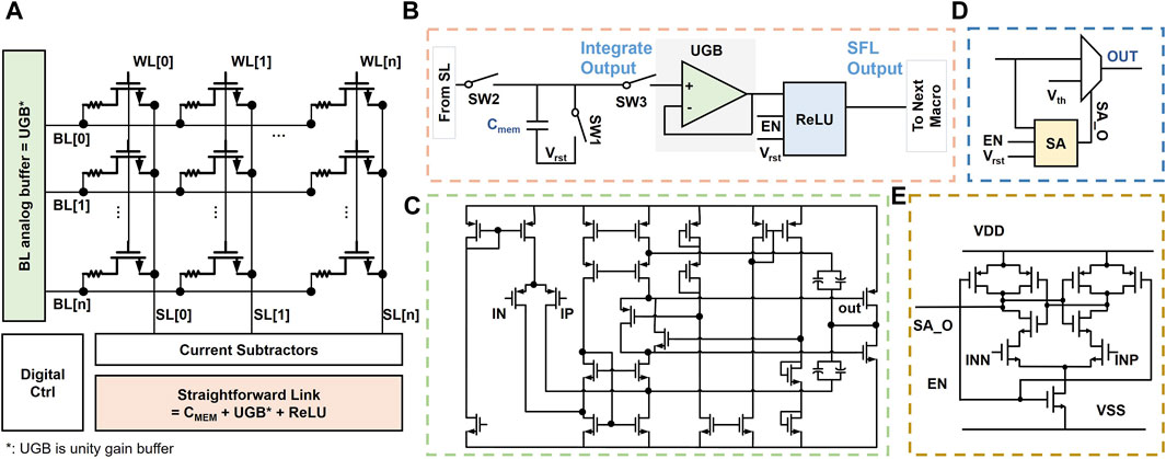
FIGURE 2. (A) ADC-less RRAM PE design; (B) schematic representation of the straightforward link (SFL). The SFL consists of a capacitor, a unity gain buffer (UGB), and a ReLU module; (C) amplifier in the UGB or BL analog buffer; (D) the ReLU module comprises a sense amplifier (SA) and a 2-to-1 MUX. (E) The SA is a latch-based voltage mode SA.
Figure 2B demonstrates the design of the SFL. It comprises a capacitor for charge-based current-to-voltage conversion, a UGB as a voltage buffer for stabilizing the voltage and driving the BLs of the next RRAM array, and a rectified linear units (ReLU) module for the activation function. Figure 2D shows the schematic representation of the ReLU module, composed of a sense amplifier (SA, as shown in Figure 2E) and a 2-to-1 multiplexer (MUX). The capacitor is used not only as a converter but also as an analog memory (CMEM). The retention time of CMEM is on the order of milliseconds, the same as DRAM, so charges in the CMEM would not reduce within 100 ns. The capacitance value needs to ensure that the range of integrated voltages is no more than the maximum read voltage, 0.2 V. In one 576 × 128 1T1R RRAM array, the subtracted currents distribute within ±11uA through algorithm evaluations. Therefore, the capacitance value is 550 fF, with an integration time of 10 ns.
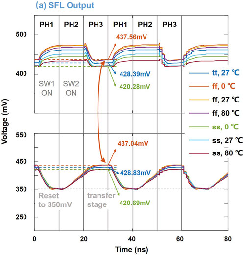
We design the SFL module in a standard 28-nm CMOS process through Cadence Virtuoso. The simulation waveforms are shown in Figure 3. In the first phase (PH1), only switch (SW) 1 is turned on and the CMEM is reset to 350 mV. In the second phase (PH2), only SW 2 is turned on and the CMEM is integrated by the subtracted current to realize the charge-based current-to-voltage conversion. In the third phase (PH3), only SW 3 is turned on and the temporarily stored voltages across the CMEM are rectified by the ReLU module and then drive the next RRAM array. The latency of the three phases is 30 ns, and each phase occupies for 10 ns. The key metric of SFL is to transfer the analog data to the next array accurately. Because analog voltages are sensitive to noise and interference, the SFL can be affected by process, voltage, and temperature (PVT) variations. We simulate the SFL under different process corners, temperatures, and supply voltages. The waveforms shown in Figure 3 demonstrate that the integrated voltages across the CMEM are transferred to the next array in all PVT situations. There is a deviation of about 0.4–0.5 mV. The total integrated noise of CMEM and UGB is 0.12 mVrms and 0.53 mVrms, respectively. The UGB offset is −65 μV, and the charge injected to CMEM is 6.29 × 10⁻¹⁹ C (about 1.1 μV). We consider all the PVT, noise, and interference in the neural network accuracy simulation and benchmark on the ResNet18/CIFAR-10. Because the one-sided swing of SFLs is 200 mV (@ tt, 27°C, and varies under different corners), the total deviation, 0.4–0.5 mV, is relatively little compared to the swing. In addition, random noise is considered during the offline training of the neural network, so the neural network can resist circuit noise after noise-aware training. Finally, neural networks also have a certain tolerance for noise. The accuracy can be maintained under noise and interference of the SFLs (as shown in Table 1).
3.2 Hierarchical architecture
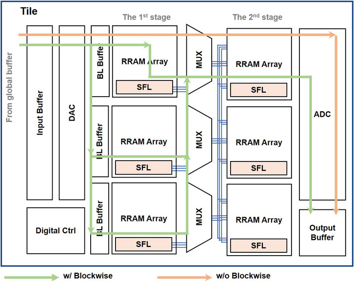
There are two levels, the PE level and Tile level, in the LINKAGE hierarchy. One Tile consists of ADC-less RRAM PEs. Figure 4 shows the Tile-level of LINKAGE architecture. There are two consecutive ADC-less PE stages, processing two continuous layers of neural networks. The PE level leverages an analog data transfer module to implement inter-array data processing. Although the LINKAGE eliminates ADC, DAC, and local buffers at the PE level, it still needs digital quantization modules at the Tile level to provide the scalability for a large-scale hierarchical system design. It needs to digitize the analog outputs and store them in global buffers for various neural network layers. The Tile of LINKAGE is designed for two consecutive layers. The first layer is mapped to the PEs of the first stage in the Tile, and the second layer is mapped to the PEs of the second stage. The pipelines in LINKAGE are organized by pairs, and two layers occupy a pipeline stage. The second layer can realize the data conversion using Tile-level ADCs to prepare the data for the next pipeline stage. In addition, large NN layers are split and mapped to multiple PEs. For the sum required after splitting, the currents can be summed by connecting two currents to the same node.
Early layers are more compute-intensive, especially the first two layers. To speed up the two most compute-intensive layers, we propose a blockwise mapping method and dataflow for LINKAGE to solve the unbalanced pipeline and communication-bound problems. First, the first two layer’s IFMs have the largest size in the plane. It will block the pipeline severely for long latency to prepare enough data for the next layers. Second, the huge inter-layer data would cause communication-bound problems. The proposed blockwise method can reuse the stored inter-layer data and largely reduce data that need to be digitalized.
Figure 5 illustrates the blockwise mapping method and dataflow. We assume that two consecutive convolutional layers are (C, K1, K1, N) and (N, K2, K2, M), where K1 and K2 are the kernel sizes, C is the input channel of the first layer, N is the input channel of the first layer and the output channel of the second layer, and M is the output channel of the second layer. At each time step, the input block moves by one stride in the IFM, as shown in Figure 5A. One subblock is the size of (C, K1, K1), the same as one kernel of the first layer. Each subblock is unfolded to a C × K1 × K1 vector to be input to a RRAM array, as shown in Figure 5B, and the array outputs N results. Similarly, the second layer needs N × K2 × K2 data; otherwise, it cannot start the complete VMM operation. To construct a balanced flow, the first layer is replicated by K2 × K2 on RRAM arrays. An input block also contains K2 × K2 subblocks, and the subblocks are staggered one stride, as shown in Figure 5C. In the first time step, the K2 × K2 subblocks are unfolded to K2 × K2 vectors and all input to RRAM arrays simultaneously. The first layer outputs N × K2 × K2 results, and they are stored in the CMEM of SFLs. Next, the results are transferred and input to the second layer through SFLs. The second layer outputs M results. At the next time step, the input block moves by one stride. K2 × (K2 -1) subblocks in this input block are the same as in the last time step. The N × K2 × (K2 -1) results of these subblocks have been stored in the CMEM of SFLs, so they need not be recalculated. Only the new K2 subblocks will be calculated, and N × K2 × 1 results are updated into CMEM. Therefore, N × K2 × K2 outputs can be calculated simultaneously at a one-time step. The N × K2 × K2 inputs of the second layer are organized through MUX sets. Each MUX is controlled by a mod-K2 synchronous counter.
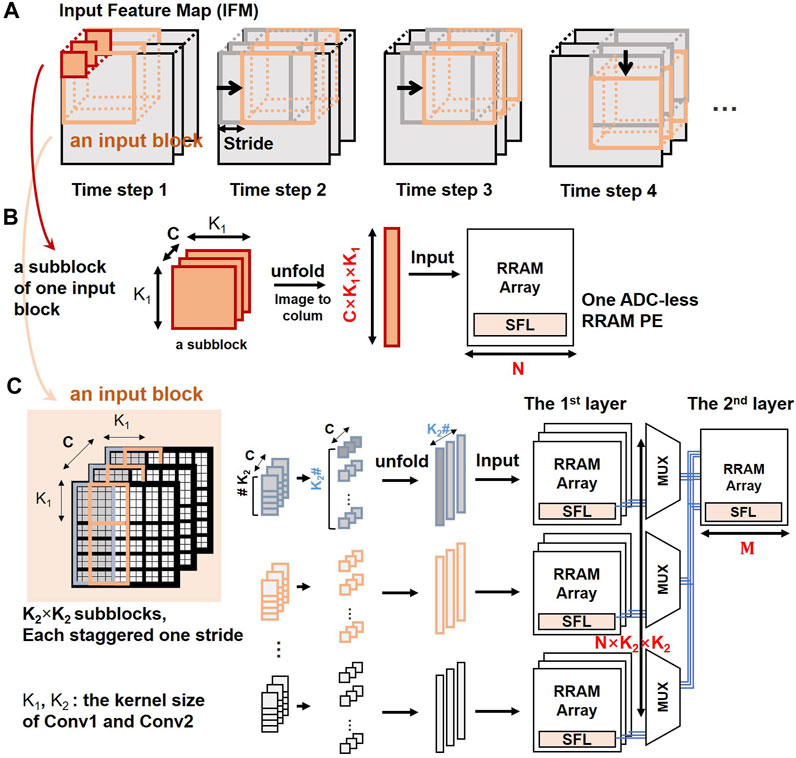
FIGURE 5. The blockwise mapping method and dataflow for two consecutive convolutional layers. (A) At each time step, the input block moves by one stride in the IFM; (B) Each subblock is unfolded and input to an ADC-less RRAM PE; (C) Only the new K2 subblocks will be calculated and N × K2 × 1 results are updated into CMEM.
Figures 6A, C illustrate the dataflow of the first two consecutive convolutional layers at the architectural level. For the first layer, Conv1, input data are loaded from input buffers to the DACs. The N × K2 × K2 outputs are obtained simultaneously from RRAM arrays in the first stage. The output currents are converted to analog voltages by the SFLs and then stored in the local analog domain. The analog voltages can be directly applied to RRAM arrays in the second stage through the SFLs. Then, the results of the second layer, Conv2, are output through the ADCs and stored first-in first-out (FIFO). It should be noted that the Tile of LINKAGE used to compute convolutional layers is designed for two consecutive layers. Otherwise, the number of replications will increase exponentially. Therefore, the convolutional layers are computed in pairs in the LINKAGE architecture. For the basic block of ResNet (Zhang et al., 2019), if there is a shortcut layer, the workflow of the shortcut layer is marked with a dotted line (as shown in Figure 6C). The currents of shortcut and conv2 can be summed by connecting the two currents to the same node. Figures 6B, D illustrate the dataflow of the other two consecutive layers. These layers of the neural network are less compute-intensive than the first two layers. It would not adopt array replication and the blockwise method.
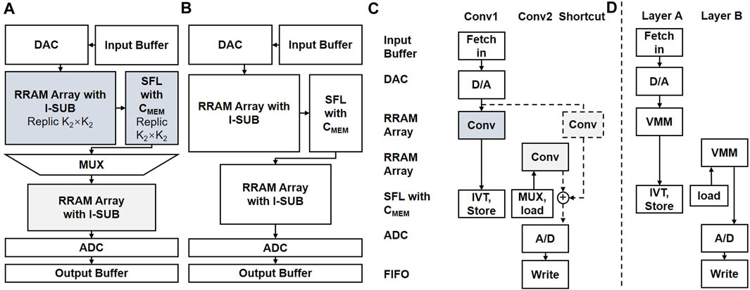
FIGURE 6. Dataflow between PEs for (A, C) two consecutive convolutional layers and (B, D) other two consecutive layers.
4 Evaluations
4.1 Experimental setup
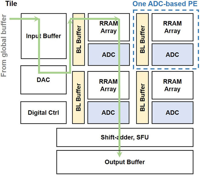
To provide a fair comparison, we build a baseline design with conventional ADC-based PE, as shown in Figure 7. This CIM architecture consists of local buffers, DACs, RRAM arrays, ADCs, shift adders, controllers, and special function units (SFUs), such as pooling units and ReLU. The analog output currents of RRAM arrays are converted to digital voltages through ADCs. Then, outputs of each part are added by a shift-adder, and the results can be stored in a local buffer as inputs to other Tiles. The DAC is shared by RRAM arrays. The 8-bit DAC would have an enormous overhead and be impossible to design, so we choose a 4-bit DAC. We retrain the NN with lower bit width weights and activations. The input and output are both 4 bits, and the weight is also 4 bits. As shown in Table 2, the accuracy loss is within 2%. We design the 4-bit ADC and 4-bit DAC modules in a standard 28-nm CMOS process. The 4-bit DAC consists of an R-ladder and clamping buffers. The R-ladder generates discrete voltages, and the clamping buffers are UGBs used to clamp the 24 analog voltage levels. In addition, each row in an RRAM array needs a BL analog buffer to drive the input voltage. One ADC is reused by eight SLs in the baseline design.
4.2 Benchmark results and discussion
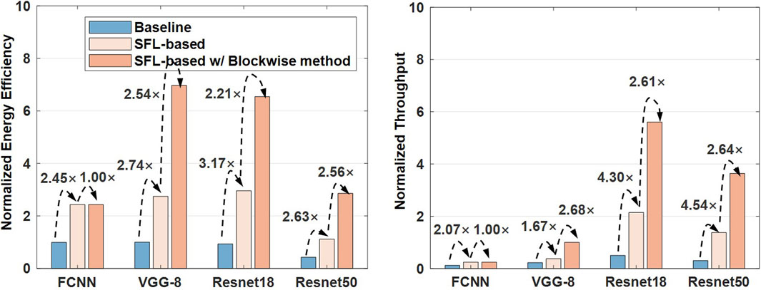
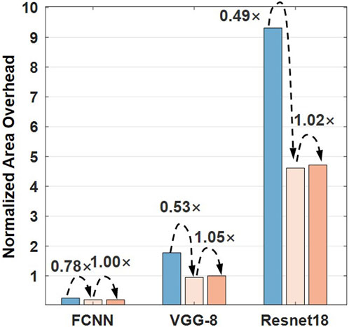
To ensure the analysis is close to the real prototype, we build an end-to-end CIM simulator with an integrated framework from the device to the algorithm. The simulator includes the noise-aware offline training algorithms, the complete design of the circuit and architecture for the RRAM neural process unit, and the non-idealities of RRAM (Liu and Gao, 2021). The performances of modules (measured from the circuit’s design) are integrated into the PE level in the LINKAGE hierarchy. For different neural networks, the performance and energy efficiency are evaluated, according to the network structure and the LINKAGE architecture. Figure 8 shows the benchmark results on FCNN/MNIST, VGG-8/CIFAR-10, and ResNet-18/CIFAR-10 and ResNet-50/CIFAR-10. The energy efficiency of proposed SFL-based designs could perform 2.45×∼3.17× better than baseline designs, and the throughput of SFL-based designs performs 1.67×∼4.30× better for different tasks. The IFMs are processed continuously inter-array without quantization, so the latency is reduced and the workloads for Tile-level ADCs are decreased. Our LINKAGE architecture can achieve 8.51∼10.35 TOPS/W energy efficiency (4b-IN/4b-W) and 0.68 ∼1.73 TOPS throughput without the blockwise method. The blockwise method can further improve the energy efficiency by 2.21×∼2.54×. LINKAGE architecture can achieve 22.9∼24.4 TOPS/W energy efficiency and 1.82 ∼4.53 TOPS throughput with the blockwise method. SFL-based designs could reduce the area by 22%–51% (Figure 9), particularly benefitted from a substantial reduction in the total number of BL buffers and ADCs at the Tile-level. In addition, the blockwise method achieves more than twice energy efficiency with little area overhead.
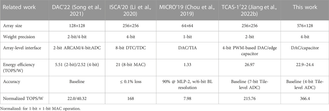
To provide a comparison, LINKAGE and other related RRAM-based CIM macros are compared, as shown in Table 3. These works also propose ADC-less solutions to solve the ADC overhead problem. We list their array-level interfacing solutions, energy efficiency, and recognition accuracy. The accuracy of these tasks is maintained to the software baseline. To intuitively compare these works, energy efficiency of macros is normalized to a 1-bit × 1-bit multiply and accumulate operation (MAC). (Input bits × weight bits × energy efficiency, or MAC bits × energy efficiency). As shown in Table 3, this work has the highest normalized energy efficiency.
5 Conclusion
In this work, we propose a CIM architecture design that eliminates PE-level ADCs. It exploits a straightforward link module that can save the inter-array analog data to the local analog domain and directly transfer analog data to the next array. Furthermore, for CNNs, we propose a blockwise dataflow to speed up compute-intensive layers and solve the unbalanced pipeline problem. To obtain accurate and reliable evaluation results, PE-level modules are designed in the standard 28-nm CMOS technology. Our LINKAGE architecture can achieve 22.9∼24.4 TOPS/W energy efficiency and 1.82 ∼4.53 TOPS throughput (4b-IN/4b-W/4b-O) with the blockwise method. The evaluation results demonstrate that the LINKAGE architecture could significantly improve the energy efficiency of CIM chips. In addition, LINKAGE provides a new type of PE and extends the search space in CIM design.
Data availability statement
The original contributions presented in the study are included in the article/Supplementary Material; further inquiries can be directed to the corresponding author.
Author contributions
YL proposed the LINKAGE architecture and performed most analyses. PY and BG checked its feasibility. PY, QL, and DW checked the function of the straightforward link module. HQ and HW conducted the studies on the RRAM arrays. QZ performed some analyses on algorithms. YL, BG, and JT prepared the manuscript. All authors contributed to the article and approved the submitted version.
Funding
This work is supported by Natural Science Foundation of China (92064001, 62025111), OPPO-THU Joint Project, IoT Intelligent Microsystem Center of Tsinghua University-China Mobile Joint Research Institute, and Beijing Advanced Innovation Center for Integrated Circuits.
Conflict of interest
The authors declare that the research was conducted in the absence of any commercial or financial relationships that could be construed as a potential conflict of interest.
Publisher’s note
All claims expressed in this article are solely those of the authors and do not necessarily represent those of their affiliated organizations, or those of the publisher, the editors, and the reviewers. Any product that may be evaluated in this article, or claim that may be made by its manufacturer, is not guaranteed or endorsed by the publisher.
References
Bayat, F. M., Prezioso, M., Chakrabarti, B., Nili, H., Kataeva, I., and Strukov, D. (2018). Implementation of multilayer perceptron network with highly uniform passive memristive crossbar circuits. Nat. Commun. 9 (1), 2331. doi:10.1038/s41467-018-04482-4
Chen, Y. H., Krishna, T., Emer, J. S., and Sze, V. (2017). Eyeriss: An energy-efficient reconfigurable accelerator for deep convolutional neural networks. IEEE J. Solid-State Circuits 52, 127–138. doi:10.1109/JSSC.2016.2616357
Chi, P., Li, S., Xu, C., Zhang, T., Zhao, J., Liu, Y., et al. (2016). “PRIME: A novel processing-in-memory architecture for neural network computation in ReRAM-based main memory,” in ACM/IEEE 43rd Annual International Symposium on Computer Architecture (ISCA), 27–39. doi:10.1109/ISCA.2016.13
Chou, T., Tang, W., Botimer, J., and Zhang, Z. (2019). “CASCADE: Connecting RRAMs to extend analog dataflow in an end-to-end en-memory processing paradigm,” in 52nd Annual IEEE/ACM International Symposium on Microarchitecture, 114–125. doi:10.1145/3352460.3358328
He, K., Zhang, X., Ren, S., and Sun, J. (2016). “Deep residual learning for image recognition,” in IEEE Conference on Computer Vision and Pattern Recognition (CVPR), 770–778. doi:10.1109/CVPR.2016.90
Jiang, H., Li, W., Huang, S., Cosemans, S., Catthoor, F., and Yu, S. (2022a). Analog-to-Digital converter design exploration for compute-in-memory accelerators. IEEE Des. Test. 39, 48–55. doi:10.1109/MDAT.2021.3050715
Jiang, H., Li, W., Huang, S., and Yu, S. (2022b). “A 40nm analog-input ADC-free compute-in-memory RRAM macro with pulse-width modulation between sub-arrays,” in IEEE Symposium on VLSI Technology and Circuits, 266–267. doi:10.1109/VLSITechnologyandCir46769.2022.9830211
Jiang, H., Huang, S., Li, W., and Yu, S. (2023). ENNA: An efficient neural network accelerator design based on ADC-free compute-in-memory subarrays. IEEE Trans. Circuits Syst. I Regul. Pap. 70, 353–363. doi:10.1109/TCSI.2022.3208755
Kiani, F., Yin, J., Wang, Z., Yang, J. J., and Xia, Q. (2021). A fully hardware-based memristive multilayer neural network. Sci. Adv. 7, 19. doi:10.1126/sciadv.abj4801
Li, W., Xu, P., Zhao, Y., Li, H., Xie, Y., and Lin, Y. (2020). “TIMELY: Pushing Data Movements and Interfaces in PIM Accelerators Towards Local and in Time Domain,” in ACM/IEEE 47th Annual International Symposium on Computer Architecture (ISCA), 832–845. doi:10.1109/ISCA45697.2020.00073
Liu, Q., Gao, B., Yao, P., Wu, D., Chen, J., Pang, Y., et al. (2020). “A fully integrated analog ReRAM based 78.4TOPS/W compute-in-memory chip with fully parallel MAC computing,” in 2020 IEEE International Solid- State Circuits Conference (ISSCC), 500–502. doi:10.1109/ISSCC19947.2020.9062953
Liu, Y., and Gao, B. (2021). “System and technology Co-optimization for RRAM based computation-in-memory chip,” in International Conference on IC Design and Technology (ICICDT) (IEEE), 1–4. doi:10.1109/ICICDT51558.2021.9626398
Qin, E., Samajdar, A., Kwon, H., Nadella, V., Srinivasan, S., Das, D., et al. (2020). “SIGMA: A sparse and irregular GEMM accelerator with flexible interconnects for DNN training,” in IEEE International Symposium on High Performance Computer Architecture (HPCA), 58–70. doi:10.1109/HPCA47549.2020.00015
Shafiee, A., Nag, A., Muralimanohar, N., Balasubramonian, R., Strachan, J. P., Hu, M., et al. (2016). “ISAAC: A convolutional neural network accelerator with in-situ analog arithmetic in crossbars,” in ACM/IEEE 43rd Annual International Symposium on Computer Architecture (ISCA), 14–26. doi:10.1109/ISCA.2016.12
Song, T., Chen, X., Zhang, X., and Han, Y. (2021). “BRAHMS: Beyond conventional RRAM-based neural network accelerators using hybrid analog memory system,” in 58th ACM/IEEE Design Automation Conference (DAC), 1033–1038. doi:10.1109/DAC18074.2021.9586247
Sze, V., Chen, Y.-H., Yang, T.-J., and Emer, J. S. (2017). Efficient processing of deep neural networks: A tutorial and survey. Proc. IEEE 105, 2295–2329. doi:10.1109/JPROC.2017.2761740
Xu, X., Ding, Y., Hu, S. X., Niemier, M., Cong, J., Hu, Y., et al. (2018). Scaling for edge inference of deep neural networks. Nat. Electron 1, 216–222. doi:10.1038/s41928-018-0059-3
Xue, C.-X., Chen, W.-H., Liu, J.-S., Li, J.-F., Lin, W.-Y., Lin, W.-E., et al. (2019). “A 1Mb multibit ReRAM computing-in-memory macro with 14.6ns parallel MAC computing time for CNN based AI edge processors,” in IEEE International Solid- State Circuits Conference (ISSCC), 388–390. doi:10.1109/ISSCC.2019.8662395
Yun, H., Shin, H., Kang, M., and Kim, L.-S. (2021). “Optimizing ADC utilization through value-aware bypass in ReRAM-based DNN accelerator,” in 58th ACM/IEEE Design Automation Conference (DAC), 1087–1092. doi:10.1109/DAC18074.2021.9586140
Zhang, W., Peng, X., Wu, H., Gao, B., He, H., Zhang, Y., et al. (2019). “Design guidelines of RRAM based neural-processing-unit: A joint device-circuit-algorithm analysis,” in 56th Annual Design Automation Conference (DAC), 1–6. doi:10.1145/3316781.3317797
Zhang, W., Gao, B., Tang, J., Yao, P., Yu, S., and Chang, M. (2020). Neuro-inspired computing chips. Nat. Electron 3, 371–382. doi:10.1038/s41928-020-0435-7
Zhou, S., Wu, Y., Ni, Z., Zhou, X., Wen, H., Zou, Y., et al. (2016). DoReFa-Net: Training low bitwidth convolutional neural networks with low bitwidth gradients. arXiv preprint arXiv: 1606.06160
Zhou, K., Zhao, C., Fang, J., Jiang, J., Chen, D., Huang, Y., et al. (2021). An energy efficient computing-in-memory accelerator with 1T2R cell and fully analog processing for edge AI applications. IEEE Trans. Circuits Syst. II Express Briefs 68, 2932–2936. doi:10.1109/TCSII.2021.3065697
Keywords: computation-in-memory, resistive random-access memory, computing-intensive, straightforward link, energy efficiency, throughput
Citation: Liu Y, Gao B, Yao P, Liu Q, Zhang Q, Wu D, Tang J, Qian H and Wu H (2023) Straightforward data transfer in a blockwise dataflow for an analog RRAM-based CIM system. Front. Electron. 4:1129675. doi: 10.3389/felec.2023.1129675
Received: 22 December 2022; Accepted: 03 April 2023;
Published: 17 April 2023.
Edited by:
Can Li, The University of Hong Kong, Hong Kong SAR, ChinaReviewed by:
Xiaoming Chen, Chinese Academy of Sciences (CAS), ChinaBing Li, Capital Normal University, China
Copyright © 2023 Liu, Gao, Yao, Liu, Zhang, Wu, Tang, Qian and Wu. This is an open-access article distributed under the terms of the Creative Commons Attribution License (CC BY). The use, distribution or reproduction in other forums is permitted, provided the original author(s) and the copyright owner(s) are credited and that the original publication in this journal is cited, in accordance with accepted academic practice. No use, distribution or reproduction is permitted which does not comply with these terms.
*Correspondence: Bin Gao, Z2FvYjFAdHNpbmdodWEuZWR1LmNu
 Yuyi Liu
 Bin Gao
 Peng Yao
 Qi Liu
 Qingtian Zhang
 Dong Wu
 Jianshi Tang
 Huaqiang Wu
