 Dong-Hyun Seo
 Baibhab Chatterjee
 Sean M. Scott2
 Shreyas Sen
- 1School of Electrical and Computer Engineering, Purdue University, West Lafayette, IN, United States
- 2Landauer, Inc., Chicago, IL, United States
This article presents the design and analysis of a resistive sensor interface with three different designs of phase noise-energy-resolution scalability in time-based resistance-to-digital converters (RDCs), including test chip implementations and measurements, targeted toward either minimizing the energy/conversion step or maximizing bit-resolution. The implemented RDCs consist of a three-stage differential ring oscillator, which is current starved using the resistive sensor, a differential-to-single-ended amplifier, and digital modules and serial interface. The first RDC design (baseline) included the basic structure of time-based RDC and targeted low-energy/conversion step. The second RDC design (goal: higher-resolution) aimed to improve the rms jitter/phase noise of the oscillator with help of speed-up latches, to achieve high bit-resolution as compared to the first RDC design. The third RDC design (goal: process portability) reduced the power consumption by scaling the technology with the improved phase-noise design, achieving 1-bit better resolution as that of the second RDC design. Using time-based implementation, the RDCs exhibit energy-resolution scalability and consume a measured power of 861 nW with 18-bit resolution in design 1 in TSMC 0.35 μm technology (with 10 ms read-time, with one readout every second). Measurements of designs 2 and 3 demonstrate power consumption of 19.2 μW with 20-bit resolution using TSMC 0.35μm and 17.6 μW with 20-bit resolution using TSMC 0.18μm, respectively (both with 10 ms read-time, repeated every second). With 30 ms read-time, design 3 achieves 21-bit resolution, which is the highest resolution reported for a time-based ADC. The 0.35-μm time-based RDC is the lowest-power time-based ADC reported, while the 0.18-μm time-based RDC with speed-up latch offers the highest resolution. The active chip-area for all three designs is less than 1.1 mm2.
1 Introduction
In recent years, low-power sensing devices have presented great potentials for many technology applications including diagnosis, physiological monitoring, and health care systems (Lorussi et al., 2004; Rairigh et al., 2009; Tavakoli et al., 2010; Lin Shu et al., 2015; Kwon et al., 2016). The pursuit of convenience for continuous monitoring in sensing applications requires these devices to have a small form of factor and low power consumption for battery-powered wearable/portable use. Thus, integrated circuits (ICs) are needed in sensing fields in order to create sensing applications. The most critical requirement of sensing devices is the accurate transmission of data/information, which requires high bit-resolution. The key challenge in designing high-resolution sensing ICs derives from system/circuit/ambient noise and power, exhibiting trade-offs among achievable resolution, noise, and power (Harrison and Charles, 2003).
1.1 Motivation and Related Works
Figure 1 shows the fundamental advantages provided by the time/frequency-mode analog-to-digital converter (ADC) over voltage/current mode ADC for low-speed and high-resolution applications in the noise- and supply voltage-limited regime. Although digital signal processors and integrated circuits take advantage of technology scaling to achieve improvements in power, speed, size, and cost, scaling of supply voltage causes a significant disadvantage to the available voltage dynamic range. In addition, the voltage/current-mode ADC interface requires signal-conditioning circuits such as analog amplifiers and filters between the sensor devices and the ADC, thus making it challenging to reduce power. Also, voltage/current-mode ADCs need sophisticated noise-canceling techniques to diminish the quantization noise as displayed in Figure 1A, which improves the signal-to-noise ratio (SNR) and bit-resolution. On the other hand, the reduction of gate delays has led an improvement in “time-resolution” in scaled devices. Furthermore, the time/frequency-mode ADC can achieve high resolution with increased enable time which can integrate residues over more time, leading to a time-domain averaging of the noise which is displayed in Figure 1B. Thus, sensing the data/information through time-based techniques (which is a time difference between two rising or falling edges) can potentially represent a better solution than sensing in voltage mode (which is a difference between two node voltages), when ADCs are implemented in a scaled process (Elsayed et al., 2011). The time-domain ADC can be as simple as a ring oscillator (that converts resistance to frequency by starving the ring oscillator with the resistive sensor), the output frequency of which can be provided to a multi-bit digital counter with a predefined enable time. The output of the counter would be a direct digital representation of the resistance.
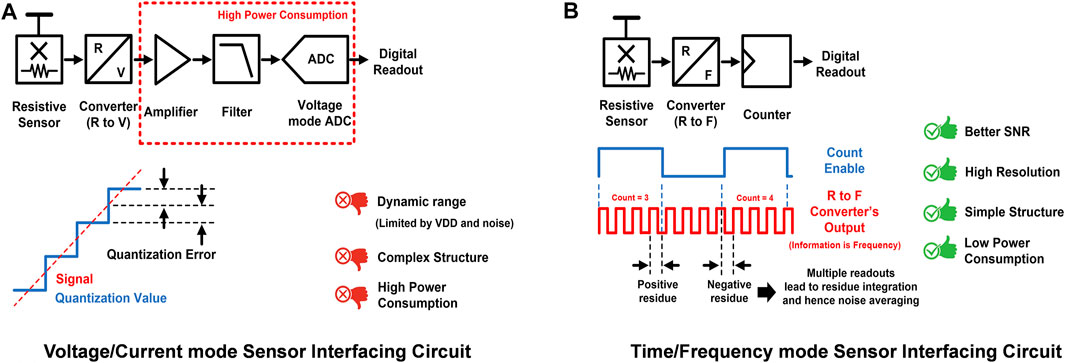
FIGURE 1. Inherent advantages provided by time/frequency-mode ADCs over voltage/current-mode ADCs for low-speed high-resolution resistive-sensing applications: (A) traditional voltage/current-mode ADC sensor-interfacing circuits and (B) time/frequency-mode ADC sensor-interfacing circuits.
Along with the popularization of sensing applications and their increasing demands, devices with low power consumption and high-resolution sensor have been increasingly preferred. Resistive sensors possess numerous strengths, including good stability, low cost, and ease to be interfaced by readout circuits. Due to these strengths, resistive sensors have been extensively practiced and utilized in diverse fields such as physiological monitoring and environmental and biomedical analysis (van den Heever et al., 2009; Gardner et al., 2010; Saxena et al., 2011; Lv et al., 2013). As devices that include a resistive sensor are widely adopted in sensing applications with diverse dynamic range requirements (such as temperature, pressure, and radiation), this article aims to analyze energy-resolution scalability of the proposed time-based resistance-to-digital converter (RDC).
1.2 Contribution
Specific contributions of this article are:
• This article presents the lowest-power and the energy/conversion step time-based RDC for low-frequency applications.
• This article presents the ways to enhance the energy-resolution trade-offs in the time-based RDC, improving the rms jitter/phase noise with help of speed-up latches, to achieve higher bit-resolution.
• This article presents the power/performance trade-off in experiment through three different design variations (optimized toward lowest energy baseline, higher resolution, and process portability), tapeout, and IC measurements.
This article is organized as follows: Section 2 describes the operating principle and system architecture of three designs of energy-resolution scalable time-based RDC. Section 3 presents the details of the circuit design with the simulation. Section 4 explains and describes the system-level simulation and result of time-based RDC. Section 5 shows experimental results of the implemented chips along with a comparison with the state of the art. Finally, concluding remarks are presented in Section 6.
2 System Architecture
Figure 2 shows the operating principle of the proposed RDC with time-based architectures that help to achieve better bit-resolution with more measurement time (Tmeas.). The proposed time-based RDC converts an input signal to a corresponding frequency and then measures this frequency over a longer period of time. It focused on maximizing the resolution and exploring the jitter-dominated resolution limit. The bit-resolution of the time-based RDC is determined by the scaled quantization error (which is the ratio of one counting cycle with the total measurement time, i.e.,
where k refers to the slope of the linearly accumulating rms jitter/phase noise with Tmeas. The bit-resolution can be defined by Eq. 2 (Chatterjee et al., 2019b).
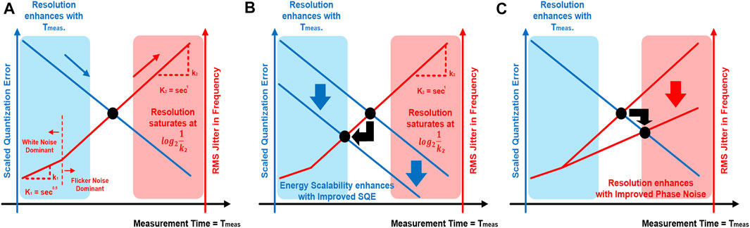
FIGURE 2. Operating principle of the time-based RDC: (A) resolution trade-offs between scaled quantization noise and jitter/phase noise of the ring oscillator in the design: quantization error decreases with time, whereas jitter accumulates with time, resulting in a saturated maximum achievable resolution in the jitter-dominated region; (B) reduction in measurement time (and hence measurement energy and energy/conversion step) by reducing the scaled quantization error of the ring oscillator;(C) improvement in resolution resulting from improving jitter/phase noise of the ring oscillator.
Even though Tmeas. increases, the bit-resolution is eventually saturated at log 2
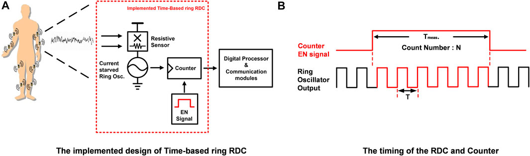
FIGURE 3. System architecture: (A) simplified diagram of time-based ring-RDC-based sensor node and (B) the timing of the RDC and counter.
The proposed time-based RDC architecture is a suitable approach for the extremely low-frequency (or effectively almost a DC quantity) signal input application. The high-oversampling ratio enabled by low-frequency input signals and by the availability of time, in modern CMOS process technology, can be leveraged to reduce the scaled quantization error (SQE) with the increased measurement time, which leads to the two key benefits, i.e., energy-resolution scalability and ultralow power.
3 Circuit Design
3.1 0.35-μm Time-Based RDC
Figure 4A shows the 0.35-μm time-based RDC, which includes resistive sensor devices that are integrated in the same chip, a current-starved three-stage differential ring oscillator (DRO), which has a tail transistor seperately for each stage, and a differential-to-single-ended amplifier in order to convert the resistance to frequency, which directly depends on the delay introduced by each inverter stage. Limiting the amount of current is a way to control the delay. In this architecture, the resistive sensors are designed in a way that the generated frequency primarily depends on the amount of current allowed by the resistance and not on other factors such as the load capacitance CL. From the concepts of impulse sensitivity function (ISF) and noise modulating function (NMF) (Hajimiri et al., 1999), the phase noise at a particular offset increases with the number of stages for a DRO with given power dissipation and frequency. In order to minimize the issues, the number of stage was fixed at a minimal required number (3) for implementation of a DRO. The phase noise for the single-ended ring oscillator (SRO), on the other hand, would not have the issue of increasing phase noise with number of stages (Hajimiri et al., 1999; Abidi, 2006).
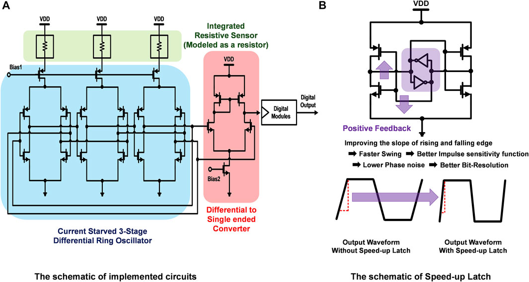
FIGURE 4. Implemented circuit schematic: (A) a resistive sensor, a current-starved three-stage differential ring oscillator, and a differential-to-singled-ended amplifier and (B) improving the slope of rising and falling edge of a three-stage ring oscillator using the speed-up latch.
However, the effects of common mode supply and substrate noise would have been more severe for the SRO because of the nonsymmetric structure. Symmetry was considered to be an important factor during layout as it contributes to minimizing the effects of supply and substrate noise. The differential-to-single-ended converter which is connected to the output of the three-stage DRO does not require voltage gain, since the input of the differential-to-single-ended converter is rail-to-rail. This means that the transconductance (gm) requirement of the differential-to-single-ended converter is small. As a result, the power consumption of the differential-to-single-ended converter is small with extremely relaxed design constraints which makes the overall design almost digital and scaling-friendly. The 0.35-um time-based RDC has the phase noise of −106.3 dBc/Hz at 1 MHz offset and oscillation frequency of 63.8 MHz with 94.4 uW non-duty cycled power consumption (when continuously on) in simulation (Chatterjee et al., 2019b).
3.2 0.35-μm Time-Based RDC With the Speed-Up Latch
Figure 4B shows how the speed-up latch is implemented with the 0.35-μm time-based RDC. The single-side band (SSB) phase noise of the DRO is defined by Eqs 3–5 (Hajimiri et al., 1999).
where η is the ratio of stage delay of rising/falling time, N is the number of DRO stages, k is the Boltzmann constant, T is temperature, P is the power dissipation, RLItail is the output swing, fo is the output frequency, and Δf is the offset frequency at which phase noise is calculated. Increasing power reduces phase noise, and reducing frequency of the operation will also reduce phase noise at a particular offset. Improving the slope of rising and falling edge of a three-stage ring oscillator enhances the phase noise performance by improving the swing. Using speed-up latches at the output of each stage of the DRO, we improve the white-noise-induced phase noise to −124.5 dBc/Hz at 1 MHz offset, as verified through simulations. The speed-up latch provides positive feedback, improving the slope of rising and falling edge of a three-stage ring oscillator as shown in Figure 4B (Baert and Dehaene, 2020).
In Figures 5A,B,C, the simulated power consumption, frequency, and phase noise are presented, respectively, as a function of the sizing of the transistors in the speed-up latch and the DRO. Since the current is limited by the resistive sensor, increasing the size of the DRO transistors capacitively loads the circuit and reduces the frequency. However, since the output of the latch provides positive feedback, the slope of output of each stage of the DRO increases (increasing the swing and frequency), which is described in Figure 5B. The phase noise improves with the level of power dissipation. However, the best design points are different in terms of power consumption, frequency, and phase noise in 0.35-μm time-based RDC with the speed-up latch. For this reason, a cost function is defined by Eq. 6.
where PN, F, and P represent the scaled linear phase noise, frequency, and power of the DRO, respectively. Reducing this cost function would mean reducing PN at a high frequency of operation but at lower power. In Figure 5D, the minimized cost function and the optimized sizing of the speed-up latch and sizing of the W/L ratio of the NMOS in the ring oscillator are presented. For the best performance, the NMOS (W/L) ratios of the speed-up latch is determined to be 4, and the NMOS (W/L) ratios of the DRO is determined to be 25 at 83.2 MHz with 1.83 mW non-duty cycled power consumption (when continuously on) in simulation. The PMOS W/L ratios are two times of the NMOS W/L ratios in both cases (DRO and speed-up latch) because both the DRO and the speed-up latch are inverter-based. The length L for design 2 is the minimum specified by the technology files.
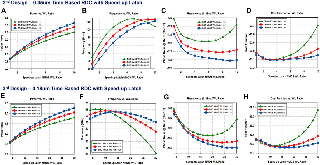
FIGURE 5. Simulation results for the time-based RDC in 0.35μm and 0.18μm technology: (A) power (design 2), (B) frequency (design 2), (C) phase noise (design 2), (D) minimization cost function vs. sizing of the DRO transistors (design 2), (E) power dDesign 3), (F) frequency (design 3), (G) phase noise (design 3), and (H) minimization cost function vs. sizing of the DRO transistors (design 3).
3.3 0.18-μm Time-Based RDC With the Speed-Up Latch
Technology scaling is the decisive factor that leads to a high-performance circuit. The threshold voltage of the device must be reduced proportionally as supply voltage reduces to sustain the output performance of the transistor. Technology scaling has also reduced the gate delay, the parasitic capacitances, and the energy and active power per transition. From Eq. 3, improving the delay of a three-stage ring oscillator enhances the phase noise performance by improving the ratio of stage delay of rising/falling time. Scaling down from 0.35μm to 0.18μm technology with the use of speed-up latches at the output of each stage of the DRO improves the power dissipation and the phase noise to 1.3 mW (when continuously on) and −130.5 dBc/Hz at 1 MHz offset, respectively, as verified through simulations. More specifically, Figures 5E,F,G show how the simulated power consumption, frequency, and phase noise change according to the size of the transistor in the speed-up latch and the DRO in 0.18 um. Compared to 0.35-μm time-based DRO with speed-up latch, power dissipation, and phase noise are improved, which accordingly improved the cost function. In Figure 5H, the minimized cost function and the optimized sizing of the speed-up latch and sizing of the W/L ratio of the NMOS in the ring oscillator are presented. For the best performance, the NMOS (W/L) ratios of the speed-up latch is determined to be 16, and the NMOS (W/L) ratios of the DRO is determined to be 25 at 61.3 MHz frequency with 1.3 mW non-duty cycled power consumption (when continuously on) in simulation. The PMOS W/L ratios are two times of the NMOS W/L ratios in both cases (DRO and speed-up latch) because both the DRO and the speed-up latch are inverter-based. The length L for design 3 is the minimum specified by the technology files.
3.4 Resistive Sensor of the Time-Based RDC
A RDC measures the resistance value of a resistive sensor, and the input range is a relevant parameter for an RDC. For determining the range of the sensing resistance, the Widlar current source configuration employed in the proposed design was analyzed. Figure 6A shows the Widlar configuration. The output current (ISS) in the saturation region is defined by Eq. 7 (Gray et al., 2001).
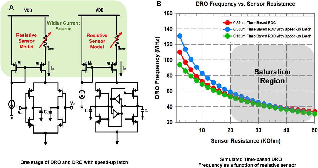
FIGURE 6. Simulation results for the time-based RDC: (A) one stage of the DRO and DRO with the speed-up latch for analysis of Rsensor range and circuit design and (B) DRO frequency as a function of Rsensor.
ISS is controlled by the resistive sensor (Rsensor), and oscillation frequency (which is a function of the delay of the ring oscillator stage, and hence a function of the current through the stage) becomes a function of Rsensor. This simulation was carried out for the strong inversion and saturation region. Figure 6B shows the DRO oscillation frequency of the 0.35-μm time-based RDC (design 1), the 0.35-μm time-based RDC with the speed-up latch (design 2), and the 0.18-μm time-based RDC with the speed-up latch (design 3) as a function of Rsensor. The oscillation frequency of DRO is saturated beyond around 20 kΩ in all three cases. Therefore, the input range of the RDCs is
In this architecture, the resistive sensors are designed in a way that the generated frequency primarily depends on the amount of current allowed by the resistance. When the values of the three resistive sensors are the same (R: fully matched scenario), the oscillation frequency would be
3.5 Digital Modules
In order to convert the change in resistance to equivalent frequency and subsequently to digital bits (Daniels et al., 2010; Sacco et al., 2020), digital modules are implemented using 24-number of D-flip-flops to count, load, and shift out a 24-bit RDC reading, as shown in Figure 7. When the enable signal is high, the flip-flops operate in the counting mode. When the enable signal is made low, the flip-flops load and shift the count value in subsequent clock cycles.
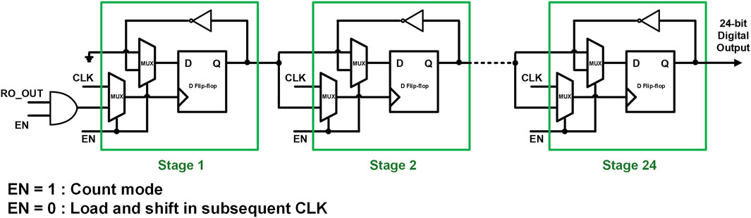
FIGURE 7. Detailed circuit schematic of digital modules with count, load, and shift modes (frequency to digital conversion).
4 System-Level Simulation
Figure 8 describes physics of the resolution limit and the corresponding simulation process. Many noise factors influence the rms jitter of this system. For example, the rms jitter of the system is all affected by flicker noise up-conversion in the tail current source and flicker noise from the correlated supply and substrate noise. The rms jitter accumulates linearly with the measurement time (Tmeas.). The linear increase in the rms jitter was theoretically shown in Hajimiri et al. (1999), Abidi (2006). However, importantly, the counting number of the rising edges of output does not linearly increase, even if the (Tmeas.) increases, primarily due to rms jitter, and which is caused by noise. This subsequently explains the resolution limit of the system, as shown in Figures 8A,B, which describe the simulation process to demonstrate the limit of the bit-resolution. Simulations are computed and verified via SpectreTM simulations using TSMC 0.35μm and 0.18μm technology. A total of 10 individual transient simulations were performed with different noise seeds. The transient noise analysis simulation includes device noise such as flicker, thermal noise, and shot noise. The maximum frequency of noise is set at 1 GHz in this simulation. The result of simulations, which refers to the rising edges of the output bits, is read at specific times. The counting numbers, represented by the 10 separate simulation results along with a different noise seed, are compared at specific times, respectively. The maximum bit-resolution can be obtained from the point in which the fluctuation of the counting numbers compared becomes severe.
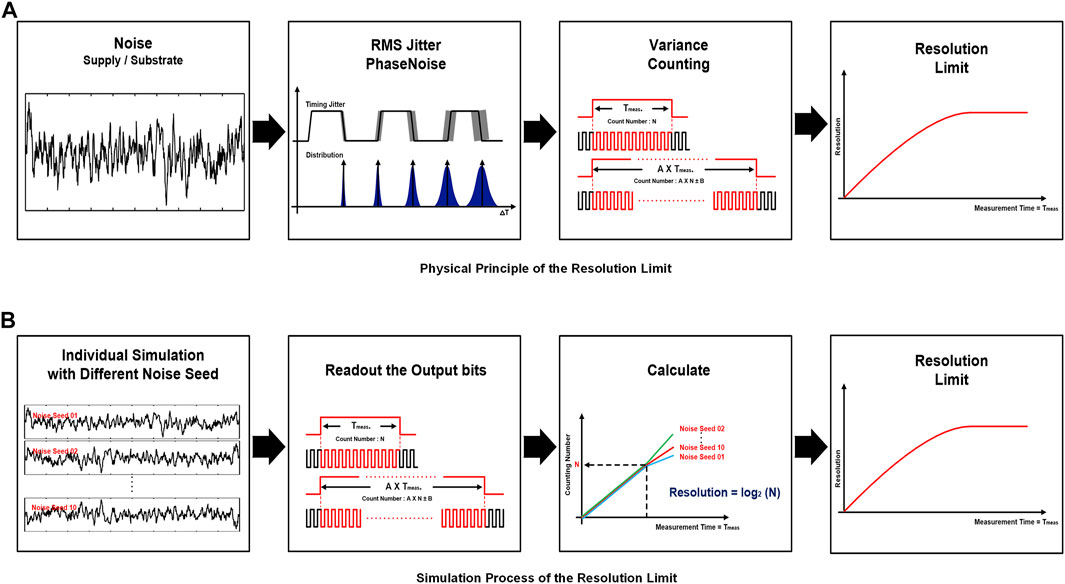
FIGURE 8. System-level simulation steps for the time-based RDC: (A) physical principle of the resolution limit and (B) simulation process to get the maximum bit-resolution.
Figure 9 shows the system-level simulation result of the 0.35-μm time-based RDC (design 1), the 0.35-μm time-based RDC with the speed-up latch (design 2), and the 0.18-μm time-based RDC with the speed-up latch (design 3). Figures 9A,D,G show that the counting number, which can be obtained from the rising edges of output, increases with the simulation time. The counting number increases, and the count value remains the same for all noise seeds with the simulation time until it reaches at a certain simulation time, 12, 20, and 35 ms. However, beyond that simulation time, the count value diverges for different noise seeds rather, and it changes randomly in all three cases. This happens for two reasons. One is that 10 different noise seeds were implemented to each individual simulation. The other is that the oscillation frequency of this system constantly changes, either by accelerating or decelerating, due to noise. In order to show the result of simulation, both the average and standard deviation of the counting number, which were derived from 10 individual transient simulations performed with different noise seeds, were calculated as shown in Figures 9B,E,H. Until the specific simulation time of 12 ms, 20, and 35 ms, the standard deviation for the counting number is zero. However, beyond that simulation time, the standard deviation increases as the simulation time increases in all three cases. The bit-resolution of the three designs of time-based RDC is plotted against the time of simulation in Figures 9C,F,I. The results show a linear increase in resolution with simulation time on log scale until they saturate in all three cases. The maximum bit-resolution can be calculated using Eq. 8
where N refers to the maximum counting number of the rising edges of output before the count value diverges for different noise seeds. This simulation shows that the maximum counting number of the rising edges of output for design 1, design 2, and design 3 is 765,959, 2,101,999, and 3,126,546, respectively. As a result, the maximum bit-resolution of design 1, design 2, and the design 3 is achieved as 19.54 bits with 12 ms, 21 bits with 20 ms, and 21.55 bits with 35 ms, respectively.
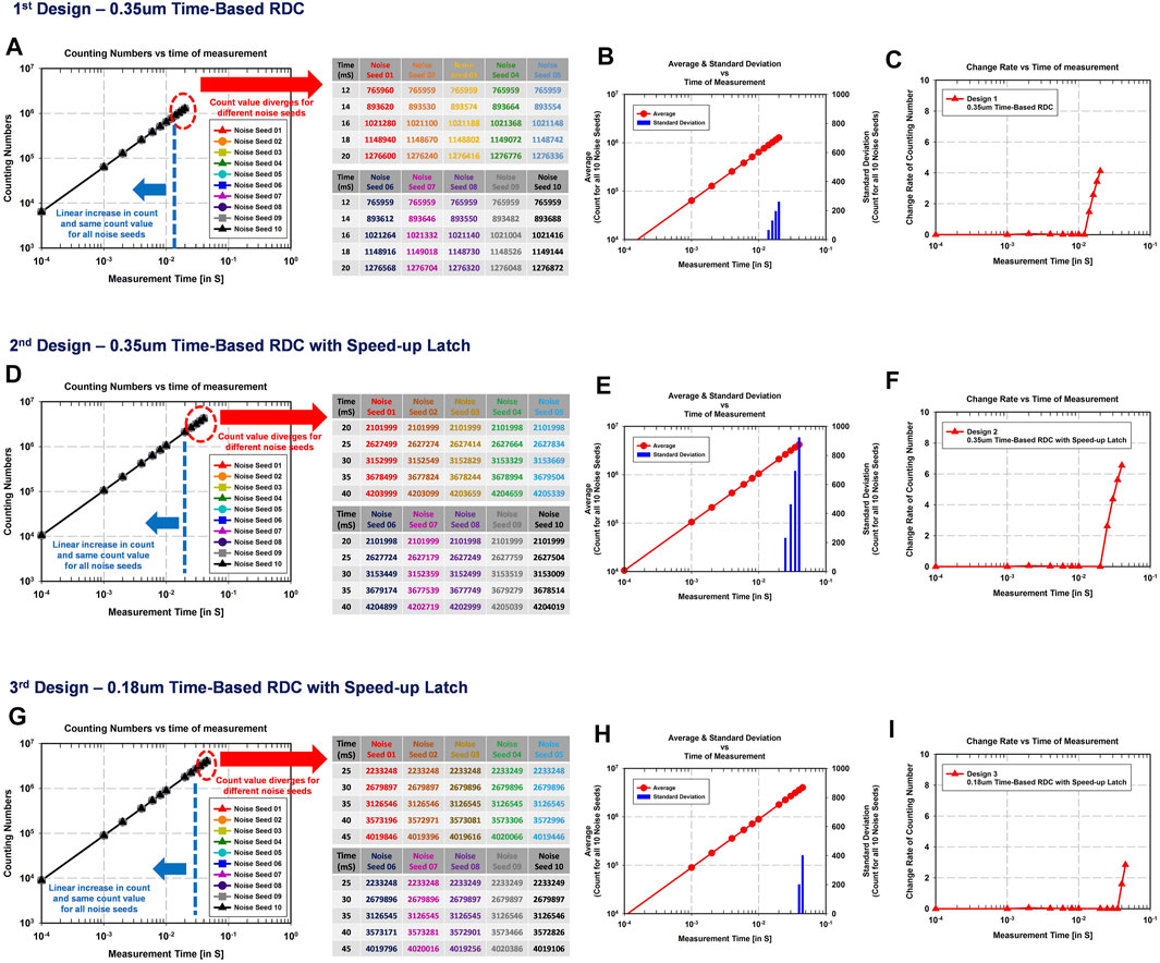
FIGURE 9. System-level simulation results for the time-based RDC: (A) 10 individual counting numbers obtained from the rising edges of output for the 0.35-μm time-based RDC (design 1), (B) average and standard deviation of counting numbers for all 10 noise seeds (design 1), (C) change rate of the counting number (design 1), (D) 10 individual counting numbers obtained from the rising edges of output for simulation of the 0.35-μm time-based RDC with the speed-up latch (design 2), (E) average and standard deviation of counting numbers for all 10 noise seeds (design 2), (f) change rate of the counting number (design 2), (G) 10 individual counting numbers obtained from the rising edges of output for simulation of the 0.18-μm time-based RDC with the speed-up latch (design 3), (H) average and standard deviation of counting numbers for all 10 noise seeds (design 3), and (I) change rate of the counting number (design 3).
Figure 10A shows the simulation results for the relationship between phase noise and energy consumption of the three designs. The phase noise from design 1 to design 3 is improved, even though energy consumption increased significantly. Based on these phase noise simulation results, the accumulated RMS jitter for integrated time can be calculated. The RMS jitter is calculated using Eq. 9 (Drakhlis, 2021).
where A refers to the integrated phase noise power, and fo is the oscillation frequency. Figure 10B plots the accumulated RMS jitter over the integrated time. The maximum achievable resolution can be calculated from the slope of the accumulated RMS jitter. The value of the slope for design 1, design 2, and design 3 is 1.88 × 10⁻⁶, 3.67 × 10⁻⁷, and 1.55 × 10⁻⁷, respectively. For calculating the average slope, two points at 0.1 and 10 ms are considered. Even though integrated time increases, the bit-resolution is eventually saturated at
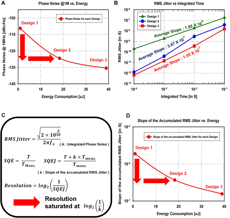
FIGURE 10. Simulation results for the three time-based RDCs: (A) phase noise vs. energy consumption, (B) the accumulated rms jitter vs. time of measurement, (C) equations, and (D) the slope of the accumulated rms jitter vs. energy consumption.
5 System-Level Measurement Results
Figure 11 describes the block diagram of the measurement setup with three designs of energy-resolution scalable time-based RDC. The implemented time-based RDC chip was measured by using the chip-on-board (COB) setup on a customized printed circuit board (PCB) with wire-bonding. The counter output represents the integer number of output cycles during one readout within the predefined measurement time Tmeas.. The measurement time signal is generated from a RIGOL DG4200 Arbitrary Waveform Generator (AWG). Alternatively, a serial interface with a microcontroller could be utilized for the readout. Since the input signal is an extremely low-frequency signal or effectively almost a DC quantity signal, standard spectrum plots used for voltage-based ADCs are not directly applicable in this case. Because there is nonlinearity in the nature of the resistance to frequency transfer function in all the three resistance-to-digital converter (RDC) designs, calibration and post-processing are required for the proposed RDC. In addition, an error due to this calibration becomes a dominant factor in the performance and linearity representation. Hence, instead of providing a standard spectrum plot for performance, we explain the method of the resolution and dynamic range measurement:
1 Resolution:
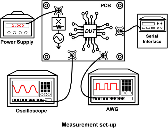
FIGURE 11. Measurement setup.
The method of resolution measurement is as follows—we take several measurements (for example, 10 measurements) each for every measurement. For a particular measurement, we record (a) integrated time of measurement and (b) calculated counting numbers. Because the input signal is an extremely low-frequency signal (effectively DC, which can be emulated by a fixed resistance in our case), we should expect the same count value for same integrated time of measurement. However, the count numbers may be different for each measurement because of jitter of the differential ring oscillator (DRO), temperature variations, voltage variations, or reference clock drift, and hence we take only the most significant bits (MSB) of the count values that remain constant over different readouts and ignore the least significant bits (LSB) that are changing over multiple measurements. This provides maximum resolution in total number of bits, starting with the first one in the MSB side, unaffected by jitter of DRO, temperature variations, voltage variations, or reference clock drift. If the counting number does not change for several measurements, the resolution is calculated by log2 (non-time varying counting number).
2 Dynamic range:
The dynamic range can be found from the range of the count value from the RDC (or the range of the frequencies with respect to the operating range of the resistive sensor). We measure the count value at a particular value of the resistive sensor in the operating range (i.e., 10 kΩ) and measure the count value at another operating point of the resistive sensor (i.e., 15 kΩ). The ratio of the total range of resistances applicable to the minimum detectable change in the resistance, when converted to dB, gives the dynamic range.
5.1 Power and Resolution
Figures 12A–C show the microphotograph and chip-on-board (COB) of the implemented 0.35-μm time-based RDC (design 1), 0.35-μm time-based RDC with the speed-up latch (design 2), and 0.18-μm time-based RDC with the speed-up latch (design 3). The active area of the chip of all three designs is less than 1.1 mm2 excluding pads. Figures 12D,E present the implemented circuit diagram of each time-based RDC. Figure 12F describes the detailed circuit schematic that consists of the speed-up latch technique. The speed-up latch improves the slope of rising and falling edge of a three-stage ring oscillator and as a result, enhances the phase noise performance by improving the swing. The bit-resolution of the three designs of time-based RDC is plotted against the time of measurement in Figures 12G–I, respectively. The results show a linear increase in resolution with measurement time on log scale for three supply voltages until they saturate as a result of jitter/phase noise accumulation. The 0.35-μm time-based RDC with the speed-up latch (design 2) increases the slope of the rising and falling edges by providing a positive feedback of the output of the latch. Compared to 0.35-μm time-based RDC (design 1), the phase noise is improved which subsequently results in higher bit-resolution. The 0.18-μm time-based RDC with the speed-up latch (design 3) reduces the power consumption for the similar readout time. As compared to design 2, 1-bit better resolution can be achieved when the readout time is increased to 30 ms. The three designs of energy-resolution scalable time-based RDC achieve 18 bit-resolution at 861nW, 20 bit-resolution at 19.1μW, and 21 bit-resolution at 52.8μW, respectively (designs 1–2 with 10 ms readout time and design 3 with 30 ms readout time, with one readout every second).
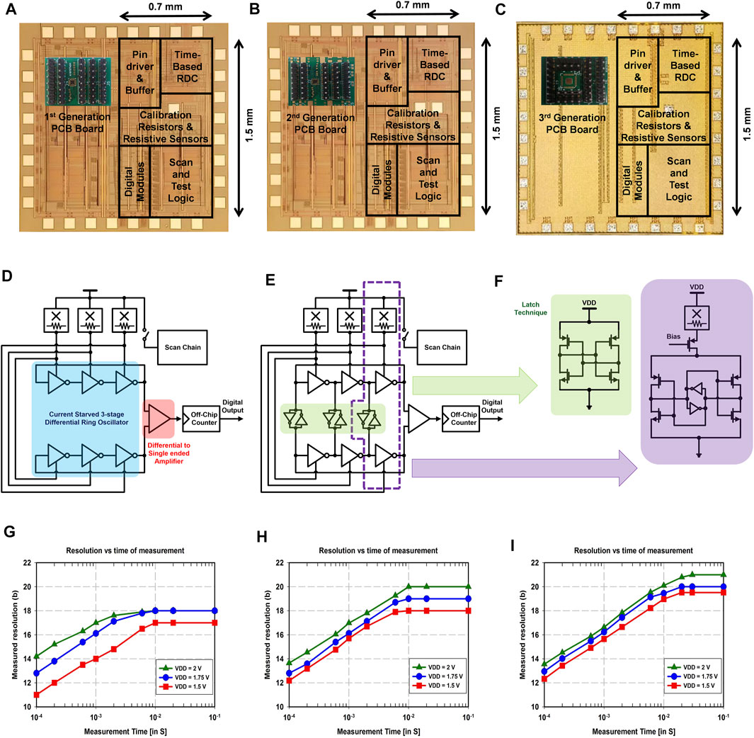
FIGURE 12. (A) Chip micrograph of the 0.35-μm time-based RDC (design 1), (B) chip micrograph of the 0.35-μm time-based RDC with the speed-up latch (design 2), (C) chip micrograph of the 0.18-μm time-Based RDC with the speed-up latch (design 3), (D) circuit diagram of 0.35-μm time-based RDC, (E) circuit diagram of the 0.35-μm and 0.18-μm time-based RDC with the speed-up latch, (F) detailed circuit schematic consisting of the speed-up latch technique, (G) resolution vs. time of measurement of the 0.35- μm time-based RDC (design 1), (H) resolution vs. time of measurement of the 0.35- μm time-based RDC with the speed-up latch (design 2), and (I) resolution vs. time of measurement of the 0.18- μm time-based RDC with the speed-up latch (design 3).
5.2 Nonlinearity
The fundamental nature of the resistance to frequency transfer function is nonlinear as shown in Chatterjee et al. (2019b), and the measured result for this transfer function for the three designs is shown in Figure 13A. From the transfer function of the three designs of RDCs, the measured resistance to frequency conversion gain at around 10 k can thus be found as 2.2834 kHz/Ω, 3.2649 kHz/Ω, and 2.3833 kHz/Ω for the 0.35-μm time-based RDC (design 1), the 0.35-μm time-based RDC with the speed-up latch (design 2), and the 0.18-μm time-based RDC with the speed-up latch (design 3), respectively. The three designs of RDCs were operated in a region in which we are using that nonlinearity to reduce the effect of the resistive sensor error. The effect of the % change in a transduced quantity (resistive sensor in this case) to output of a time-based ADC is nonlinear correspondence and calibration and post-processing are required for the proposed RDC. With calibration and with a static tolerance in the transducer, the error is negligible. When the transducer has a dynamic variation without any variation in the input quantity, i.e., if the transducer has a dynamically varying % error–it will affect the achievable resolution as shown in Figure 13B. However, a large dynamic error (
1 Per-device off-line calibration:
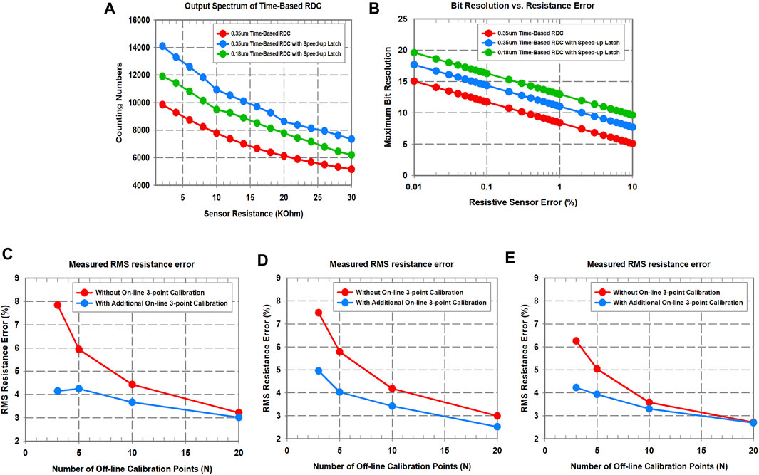
FIGURE 13. (A) Measured resistance to frequency transfer function of the three RDC designs, (B) maximum achievable bit-resolution with respect to resistive sensor error of the three RDC designs, (C) measured RMS resistance error (%) for per-device off-line calibration, followed by online three-point calibration for the 0.35-μm time-based RDC (design 1), (D) measured RMS resistance error (%) for per-device off-line calibration, followed by online three-point calibration for the 0.35-μm time-based RDC with the speed-up latch (design 2), and (E) measured RMS resistance error (%) for per-device off-line calibration, followed by online three-point calibration for the 0.18-μm time-based RDC with the speed-up latch (design 3).
This requires finding out the resistance to frequency transfer function for each device during a pre-measurement (off-line) calibration and applying the inverse of that function during measurement to correct for the nonlinearity. This method would result in better accuracy as the number of points used for calibration increases. In the limiting case, the error will tend to zero (resulting in extremely high linearity) as the number of points approaches infinity. However, this incurs a high amount of cost in terms of time and available manual resources.
2 Per-batch off-line calibration followed by an online calibration:
This requires finding out the resistance to frequency transfer function off-line, for one device out of a batch of devices, and eventually updates the transfer function for each device online during measurement to take care of PVT (process, voltage, and temperature) variations. However, the results might be largely inaccurate due to small number of online data points for calibration and large process variations.
3 Subset of per-device off-line calibration followed by an online calibration:
As a compromise between methods 1 and 2, we can perform per-device off-line calibration with a reduced number of points (that will lower the test cost) and then perform an online update of the transfer function during measurement to take care of the VT (voltage and temperature) variations.
Figures 13C–E show the measured RMS resistance error (%) for per-device off-line calibration, followed by on-line three-point calibration for three designs. For calculating the RMS resistance error, five frequency points were randomly selected from all frequencies which correspond to resistances within the 2 kΩ–50 kΩ range. The inverse of the resistance to frequency transfer function was applied on these frequencies to find out the resistance. This resistance is compared with the original resistance values to find the RMS error (%) for the five points. During this process, the points used for calibration and for test were always kept separate. The number of off-line calibration points is varied from 3 to 20, while the number of online calibration points is set to 3 (which is a feature of all 3 designs and is shown in detail in Chatterjee et al. (2019b). With the additional automatic online calibration, the number of points required for off-line calibration reduces for the similar amount of the rms error.
5.3 Power Supply Noise
Among the factors that degrade the phase noise performance of oscillators, power supply noise is one of the most dominant factors in terms of its effect on both the frequency and phase of the oscillator. The power supply voltage affects the delay of the ring oscillator. In a current-starved ring oscillator, the power supply noise will reflect as current fluctuations. Figure 14 shows the bit-resolution of the time-based RDC with respect to the power supply noise amplitude. As the amplitude of the power supply increases, the bit-resolution decreases for all the designs. However, even with 10mV peak-to-peak supply noise, the resolution of the designs 2 and 3 of RDCs remains
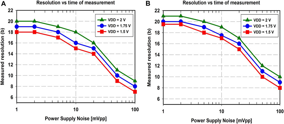
FIGURE 14. Resolution vs. supply noise measurement of (A) 0.35-μm time-based RDC with the speed-up latch (design 2) and (B) 0.18-μm time-based RDC with the speed-up latch (design 3), showing
5.4 Energy-Resolution Scalability
Table 1 summarizes the performance of the three designs of energy-resolution scalable time-based RDC in comparison with state-of-the-art high-resolution time-based ADC architectures. The 0.35-μm time-based RDC consumes the lowest energy, which is 861 nJ with 10 ms, among all ADCs, and the 0.18-μm time-based RDC with the speed-up latch offers the highest resolution, which is 21-bit with 30 ms, among all ADCs. From the perspective of the energy/conversion step, the 0.35-μm time-based RDC shows the best performance which is 3.29 pJ/bit, among all ADCs. This can be achieved because the proposed time-based RDC architecture enabled by low-frequency input signals and by the availability of time can be leveraged to reduce the scaled quantization error (SQE) with the increased measurement time, which leads to the two key benefits, i.e., energy-resolution scalability and ultralow power. This work, for the first time, explores the process scalability and shows the measured limits for such designs.
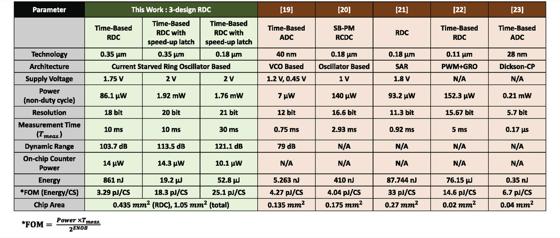
TABLE 1. Measured performance summary of the three-design time-based RDC and comparison table
6 Conclusion
In this article, we presented the design and analysis of a resistive sensor with three designs of the energy-resolution scalable time-based resistance-to-digital converter (RDC) with test chip implementations and measurements. The implemented RDC consisted of a current-starved differential ring oscillator, a differential-to-single-ended amplifier, and an off-chip counter in order to convert the change in resistance to equivalent frequency. This article presents that the 0.35-μm time-based RDC is the lowest-power time-based ADC reported till date, while the 0.18-μm time-based RDC with the speed-up latch offers the highest resolution which is the way to enhance the energy-resolution trade-off in the time-based RDC, improving the rms jitter/phase noise with help of speed-up latches, to achieve higher bit-resolution. Insights into the energy-resolution trade-offs, scalability aspects, and effects of power supply noise are also discussed in the article. We wanted to explore the power/performance trade-off in experiment through three different design variations, tapeout, and IC measurements. As a future work, to improve the scaled quantization error would be explored using the multiphase of the ring-oscillator, (Watanabe and Terasawa, 2010; Pepe and Andreani, 2019), thereby improving the energy/conversion step.
Data Availability Statement
The raw data supporting the conclusion of this article will be made available by the authors, without undue reservation.
Author Contributions
D-HS, BC, SMS, DV, DP, and SS contributed to the conception and design of the study, experiments, and writing. All authors contributed to manuscript revision and read and approved the submitted version.
Conflict of Interest
SS and DV were employed by the company Landauer, Inc.
The remaining authors declare that the research was conducted in the absence of any commercial or financial relationships that could be construed as a potential conflict of interest.
Publisher’s Note
All claims expressed in this article are solely those of the authors and do not necessarily represent those of their affiliated organizations, or those of the publisher, the editors, and the reviewers. Any product that may be evaluated in this article, or claim that may be made by its manufacturer, is not guaranteed or endorsed by the publisher.
References
Abidi, A. A. (2006). Phase Noise and Jitter in CMOS Ring Oscillators. IEEE J. Solid-State Circuits 41 (8), 1803–1816. doi:10.1109/jssc.2006.876206
Baert, M., and Dehaene, W. (2020). A 5-GS/s 7.2-ENOB Time-Interleaved VCO-Based ADC Achieving 30.5 fJ/cs. IEEE J. Solid-States Circuits 55 (6), 1577–1587. doi:10.1109/JSSC.2019.2959484
Chatterjee, B., Mousoulis, C., Maity, S., Kumar, A., Scott, S., Valentino, D., et al. (2019). “A Wearable Real-Time CMOS Dosimeter with Integrated Zero-Bias Floating-Gate Sensor and an 861nW 18-bit Energy-Resolution Scalable Time-Based Radiation to Digital Converter,” in 2019 IEEE Custom Integrated Circuits Conference (CICC), Austin, TX, April 14–17, 2019.
Chatterjee, B., Mousoulis, C., Seo, D. -H., Maity, S., Kumar, A., Scott, S., et al. (2019). A Wearable Real-Time CMOS Dosimeter with Integrated Zero-Bias Floating Gate Sensor and an 861nW 18-bit Energy-Resolution Scalable Time-Based Radiation to Digital Converter. IEEE J. Solid-States Circuits 55 (3), 650–665. doi:10.1109/JSSC.2019.2953833
Daniels, J., Dehaene, W., Steyaert, M., and Wiesbauer, A. (2010). “A A 0.02 Mm2 65nm CMOS 30MHz BW All-Digital Differential VCO-Based ADC with 64dB SNDR,” in 2010 IEEE Symposium on VLSI Circuits, Honolulu, HI, June 15–17, 2010.
Drakhlis, B. (2021). Calculate Oscillator Jitter by Using Phase-Noise Analysis. Microwaves and RF, 109–119.
Elsayed, M. M., Dhanasekaran, V., Gambhir, M., Silva-Martinez, J., and Sanchez-Sinencio, E. (2011). A 0.8 Ps DNL Time-To-Digital Converter with 250 MHz Event Rate in 65 Nm CMOS for Time-Mode-Based ΔΣ Modulator. IEEE J. Solid-State Circuits 46 (9), 2084–2098. doi:10.1109/jssc.2011.2156990
Esmailiyan, A., Du, J., Siriburanon, T., Schembari, F., and Staszewski, R. B. (2021). Dickson-Charge-Pump-Based Voltage-To-Time Conversion for Time-Based ADCs in 28-nm CMOS. IEEE Open J. Circuits Syst. 2, 23–31. doi:10.1109/ojcas.2020.3043094
Gardner, J. W., Guha, P. K., Udrea, F., and Covington, J. A. (2010). CMOS Interfacing for Integrated Gas Sensors: A Review. IEEE Sensors J. 10 (12), 1833–1848. doi:10.1109/jsen.2010.2046409
George, A. K., Shim, W., Je, M., and Lee, J. (2018). “A 114-AF RMS- Resolution 46-NF/10-MΩ -Range Digital-Intensive Reconfigurable RC-To-Digital Converter with Parasitic-Insensitive Femto-Farad Baseline Sensing,” in 2018 IEEE Symposium on VLSI Circuits, Honolulu, HI, June 18–22, 2018.
Gray, P., Meyer, R., Hurst, P., and Lewis, S. (2001). Analysis and Design of Analog Integrated Circuits. 4th. Ed. , NY, USA: John Wiley & Sons.
Hajimiri, A., Limotyrakis, S., and Lee, T. H. (1999). Jitter and Phase Noise in Ring Oscillators. IEEE J. Solid-State Circuits 34 (6), 790–804. doi:10.1109/4.766813
Han, H., Choi, W., and Chae, Y. (2019). “A 0.02 Mm2 100dB-DR Impedance Monitoring IC with PWM-Dual GRO Architecture,” in 2019 IEEE Symposium on VLSI Circuits, Kyoto, Japan, June 9–14, 2019.
Harrison, R. R., and Charles, C. (2003). A Low-Power Low-Noise Cmos for Amplifier Neural Recording Applications. IEEE J. Solid-State Circuits 38 (6), 958–965. doi:10.1109/jssc.2003.811979
Jiang, W., Hokhikyan, V., Chandrakumar, H., Karkare, V., and Markovic, D. (2017). A ±50-mV Linear-Input-Range VCO-Based Neural-Recording Front-End with Digital Nonlinearity Correction. IEEE J. Solid-State Circuits 52 (1), 173–184. doi:10.1109/jssc.2016.2624989
Kwon, J.-W., Jin, D. -H., Kim, H.-J., Hwang, S.-I., Shin, M.-C., Cheon, J.-H., et al. (2016). A Low-Power TDC-Configured Logarithmic Resistance Sensor for MLC PCM Readout. IEEE Sensors J. 16 (14), 5524–5535. doi:10.1109/jsen.2016.2572207
Lee, B., Kim, H., Kim, J., Han, K., Cho, D.-I. D., and Ko, H. (2018). A Low-Power 33 pJ/Conversion-Step 12-bit SAR Resistance-To-Digital Converter for Microsensors. Microsyst Technol. 25 (5), 2093–2098. doi:10.1007/s00542-018-4229-z
Lin Shu, L., Xiaoming Tao, X., and Feng, D. D. (2015). A New Approach for Readout of Resistive Sensor Arrays for Wearable Electronic Applications. IEEE Sensors J. 15 (1), 442–452. doi:10.1109/jsen.2014.2333518
Lorussi, F., Rocchia, W., Scilingo, E. P., Tognetti, A., and De Rossi, D. (2004). Wearable, Redundant Fabric-Based Sensor Arrays for Reconstruction of Body Segment Posture. IEEE Sensors J. 4 (6), 807–818. doi:10.1109/JSEN.2004.837498
Lv, J., Zhong, H., Zhou, Y., Liao, B., Wang, J., and Jiang, Y. (2013). Model-Based Low-Noise Readout Integrated Circuit Design for Uncooled Microbolometers. IEEE Sensors J. 13 (4), 1207–1215. doi:10.1109/jsen.2012.2230621
Pepe, F., and Andreani, P. (2019). An Accurate Analysis of Phase Noise in CMOS Ring Oscillators. IEEE Trans. Circuits Syst.66 (8), 1292–1296. doi:10.1109/tcsii.2018.2884569
Rairigh, D. J., Warnell, G. A., Xu, C., Zellers, E. T., and Mason, A. J. (2009). CMOS Baseline Tracking and Cancellation Instrumentation for Nanoparticle-Coated Chemiresistors. IEEE Trans. Biomed. Circuits Syst. 3 (5), 267–276. doi:10.1109/tbcas.2009.2023511
Sacco, E., Vergauwen, J., and Gielen, G. (2020). A 16.1-bit Resolution 0.064-mm2 Compact Highly Digital Closed-Loop Single-VCO-Based 1-1 Sturdy-MASH Resistance-To-Digital Converter with High Robustness in 180-nm CMOS. IEEE J. Solid-state Circuits 55 (9), 2456–2467. doi:10.1109/jssc.2020.2987692
Saxena, R. S., Saini, N. K., and Bhan, R. K. (2011). Analysis of Crosstalk in Networked Arrays of Resistive Sensors. IEEE Sensors J. 11 (4), 920–924. doi:10.1109/jsen.2010.2063699
Tavakoli, M., Turicchia, L., and Sarpeshkar, R. (2010). An Ultra-Low-Power Pulse Oximeter Implemented with an Energy-Efficient Transimpedance Amplifier. IEEE Trans. Biomed. Circuits Syst. 4 (1), 27–38. doi:10.1109/tbcas.2009.2033035
van den Heever, D. J., Schreve, K., and Scheffer, C. (2009). Tactile Sensing Using Force Sensing Resistors and a Super-Resolution Algorithm. IEEE Sensors J. 9 (1), 29–35. doi:10.1109/jsen.2008.2008891
Keywords: resistive sensor, sensor interfacing circuit, resistance-to-digital converter, time-based ADC, low-power, RMS jitter, low-phase noise, energy-resolution scalability
Citation: Seo D-H, Chatterjee B, Scott SM, Valentino DJ, Peroulis D and Sen S (2022) Design and Analysis of a Resistive Sensor Interface With Phase Noise-Energy-Resolution Scalability for a Time-Based Resistance-to-Digital Converter. Front. Electron. 3:792326. doi: 10.3389/felec.2022.792326
Received: 10 October 2021; Accepted: 28 February 2022;
Published: 25 April 2022.
Edited by:
Masahiro Fujita, The University of Tokyo, JapanReviewed by:
Hitesh Shrimali, Indian Institute of Technology Mandi, IndiaAnkesh Jain, Indian Institute of Technology Delhi, India
Copyright © 2022 Seo, Chatterjee, Scott, Valentino, Peroulis and Sen. This is an open-access article distributed under the terms of the Creative Commons Attribution License (CC BY). The use, distribution or reproduction in other forums is permitted, provided the original author(s) and the copyright owner(s) are credited and that the original publication in this journal is cited, in accordance with accepted academic practice. No use, distribution or reproduction is permitted which does not comply with these terms.
*Correspondence: Dong-Hyun Seo, c2VvNjBAcHVyZHVlLmVkdQ==