 Saleem Khan
 Shawkat Ali1
 Tareq Al-Ansari
- 1Division of Information and Computing Technology, College of Science and Engineering, Hamad Bin Khalifa University, Doha, Qatar
- 2Division of Sustainable Development, College of Science and Engineering, Hamad Bin Khalifa University, Doha, Qatar
This paper presents a comparative study on the treatment techniques for flexible polymeric substrates and their impact on the printing results. Substrate treatments are central to optimization of the printing processes and a strict set of requirements are needed to achieve uniform and acceptable printing results. Therefore, this research is highlighting the most significant treatment methods used for fine-tuning the surface properties of different polymeric substrates. Besides the two commonly used treatment techniques of oxygen plasma and ultraviolet ozone, a new method of using surface cleaning liquid is applied for rapid treatment of polymeric substrates. Comparative study is carried out on the basis of cleaning steps required for substrate preparation, processing, robustness as well as on the final printed results on the substrates. All the three treatment techniques with similar processing protocol are applied on a single type of polyimide (PI) substrate. To further validate the applicability and manufacture of practical devices, the liquid cleaning method is also applied on Polyethylene terephthalate substrates for making proof-of-concept wearable temperature sensor. From the study it is concluded that the liquid surface cleaning method is advantageous in terms of easy processing, robustness and producing uniform printing results on diverse polymeric substrates.
Introduction
Printed electronics is a fast-emerging field for manufacturing of unconventional electronic components, which are ideal for deployment on large areas and nonplanar surfaces as well as for portable applications (Khan et al., 2014; Suganuma, 2014; Khan et al., 2020). The prominent features such as flexibility, stretchability and foldability etc. are enabled primarily by the polymeric based plastic substrates and solution based functional nanomaterials (Wang and Liu, 2016). The latest developments in functional nanomaterials (both organic and inorganic) and their processing from solutions with the help of inkjet printing technologies have contributed significantly to producing flexible electronics. The reliable integration of printed materials, performance, efficiency, and durability of flexible electronics is determined by the quality and properties of the polymeric substrates (Huang and Zhu, 2019; Wiklund et al., 2021). Therefore, these substrates are desired to meet the specific requirements and withstand the chemical, physical and mechanical properties of the functional materials deposited on top of its surface (Malik and Kandasubramanian, 2018; Palavesam et al., 2018; Khan et al., 2019).
Functional nanomaterials available in the form of colloidal suspensions or mixtures of hybrid organic-inorganic nanocomposites are tuned to be efficiently used with the desired printing technology. Thin film deposition of functional nanomaterials through printing technologies requires a wide range of optimization parameters (Kamyshny and Magdassi, 2014; Huang and Zhu, 2019; Wiklund et al., 2021). The uniformity in thicknesses and coverage area of thin films, as well as the consistency in producing patterns with uniform linewidths are highly desired. These acceptable printed results are achieved successfully through optimization of multiple approaches i.e. printing system parameters, rheological properties of the inks and finally the substrate treatments (Aleeva and Pignataro, 2014; Wiklund et al., 2021). Majority of the researches reported about optimization of printing technologies, focus on the manufacturing processes and rheological properties of nanomaterial suspension. However, beside these, surface treatment of the substrates is also of particular interest as uniform spreading and patterning of the deposited materials in a controlled fashion is greatly dependent on the surface properties of the substrate (Nemani et al., 2018). Quality and resolution of the printed thin film structures is influenced by the substrate surface properties such as work of adhesion, wettability and surface energy etc. determining how the ink will interact at the interface and spread over the substrate (Meng et al., 2019; Aydemir et al., 2021).
Various techniques have been developed for tuning the surface properties of the substrates ideal for uniform thin film deposition and patterning. Few of the commonly used treatment techniques are corona discharge, plasma treatment and chemicals-based surface modifications etc. (Verkuijlen et al., 2014; Nemani et al., 2018; Haq et al., 2019). The corona discharge method is used to ionize an entrapped gas in a closed chamber and high electric field applied between the two conducting electrodes. By impacting the substrate surface, energy from the ions is transferred to the surface molecules and thus making the surface ideal for the functional nanomaterials to adhere strongly (Haq et al., 2019). Various functional groups developed on the substrate surface are hydroxyl, peroxyl, carbonyl, ester, carboxylic acid, which play significant role in tuning the receiving surface properties for deposited nanomaterials. Oxygen plasma on the other hand is broadly used for surface treatment of substrates, as it offers marginal advantages over other techniques (Banerjee et al., 2018; Kim et al., 2018). The ease in operation, safety, less regents’ requirements, applicability to a wide range of substrates including low Tg (glass transition) and uniform modification of the surface energies make it more appealing. Among these, chemical bases treatment has been claimed to be cheaper and readily available solution for such surface modifications. Chemical treatment is ideally required for water-based solution and particularly for binding biomolecules on polymeric substrates (Schlisske et al., 2018; Santidrián et al., 2019). Carboxylic acid groups are created on the surface of polymer substrates as a result of chemical modification that enhances the attachment of bioactive molecules such as proteins onto the surface. Various chemicals such as 2-(butoxyetoxy) ethanol, KMnO4, NaOH, K2Cr2O7, H2SO4 etc. are used at mixing with different concentrations (Villani et al., 2009; Mäntysalo et al., 2012; Nemani et al., 2018). The substrates are kept immersed at specific times sometime for hours to reach the desired level of surface functionality. In this research we have explored a new and very robust technique to functionalize various substrates at ambient conditions. The commercially available Reztore ESD surface cleaner is used as the main treatment solution. Reztore is a commonly used cleaning liquid specially to remove dust, grease, stains, and solder flux etc. from a wide variety of surfaces. Three functionalization techniques i.e. oxygen plasma, UV plasma and wet chemical treatments are applied on polyimide (PI) substrates and results are compared. The wet chemical cleaner is also applied on PET and cellulose based biodegradable substrate to justify their use for a wide variety of substrates. Inkjet printing is applied for all the experiments and metallic nanoparticles-based ink is used for the printing purposes. Physical, optical, and electrical properties are determined, and a comparative study is performed. A temperature sensor is also developed as proof-of-concept device using the biocompatible substrate. The sensor is tested in the temperature ranges ideal for wearable temperature sensing applications. The sensor is tested in the range of 25–45°C, that showed promising results by producing linear response in the electrical resistance against the temperature rise. These sensors with complementary signal processing circuits and wireless communication modules would greatly help in realizing wearable temperature sensors with enhanced fabrication protocols.
Materials and Methods
Ink for the Printing Tests
Comparative study is performed considering only the surface treatments of the substrates. This requires rest of the influencing parameters to remain same and therefore, a single type of ink was used without making any changes to the composition. Commercially available silver (Ag) (Sigma Aldrich) nanoparticles-based ink was used. Rheological properties of the ink are pre-adjusted that are suitable for the drop-on-demand inkjet printing system. The solid content of nanoparticles is in the range of 30–35% of the colloidal solution. Sintering temperature of the ink is 120 C as per supplier recommendations, which is in matching with the working temperatures of the polymeric substrates.
Substrates Preparation
Three different types of polymeric substrates are selected for the two set of experiments. Polyimide (PI) is a high thermally stable substrate and is used here for the central comparative study based on different treatment mechanisms. Whereas PET and cellulose based polymeric substrate are used to test and further validate the newly explored functionalization technique. Before surface activations, the substrates were properly cleaned using standard rinsing procedure. The substrate was emersed in acetone and isopropanol for 10 min subsequently and then rinsed with DI water. The substrate was kept in oven at 100 °C for 15 min as a final dehydration step. Oxygen plasma, UV ozone and wet chemical cleaning are applied on PI substrates independently. Three sets of substrates were prepared to use for each of the surface activation process. The treatment parameters applied here are already optimized to achieve acceptable panting results. In first case of oxygen plasma, 25% of the power for 10 s was performed using Zepto plasma system (13.6 kHZ with a power range of 0–50 W). Secondly, for the UV ozone activation, the system (Ossila) used is based on fixed specifications of lamp power, intensity, and wavelengths. The tunable parameter in such systems is based on the duration of exposure time. The system is equipped with synthetic Quartz UV grid lamp with dominant wavelengths of 185 and 254 nm. The lamp with 30 mA current produces an output intensity of 20 μW/cm2. To functionalize the surface, the substrate was kept for 2 min under UV ozone at these described specifications. Finally for the wet treatment, the Reztore (ESD surface cleaner) was spray coated on PI substrate, left over for 30 s, and dried immediately with a cotton wipe similar to a normal cleaning procedure. The substrate was kept on a hotplate at 45°C, this removes any residual vapors or nanolayers left behind after wiping out the cleaner. The printing process was performed immediately right after surface treatments of the substrates.
Contact Angle Analyzer
Contact angle is an important parameter used to determine the surface properties of substrates. It is the angle between the tangent of the droplet’s profile and tangent to the intersecting points on the surface concerning vapor, liquid and solid (Meiron et al., 2004; Cwikel et al., 2010). The surface energies of the substrate interfacing point of the solid and liquid medium qualifies to what extent the colloidal solution will wet the target surface. Figure 1 shows representative pictures of the wetting and non-wetting surfaces. The uniform spreading and homogeneous thin film deposition is highly desired for printed patterns, which is partly determined by the surface properties of the substrate. The substrate surfaces are termed as hydrophilic or hydrophobic determined exclusively by the contact angle of the impacting droplet. Conventionally, if the contact angle is less than 90o, the surface is considered as hydrophilic and have a strong wetting behavior whereas, for a higher contact angle i.e. > 90o, the surface becomes hydrophobic. In this scenario, a compromising value within the range of 62-78o is more suitable for inkjet printing systems to achieve the most optimal results. Treating and achieving these ranges is also accompanied by the surface roughness values that also contribute significantly to the uniform distribution of ink deposited from droplet ejection systems. The essential surface properties such as contact angle, work of adhesion, wetting energy, and surface tension of the solution was determined by using contact angle analyzer. The system is equipped with high-speed camera to analyze the droplet interaction with the surface starting from the first instance of contact until reaching equilibrium, where the force balance is attained at the interface of the droplet and substrate.
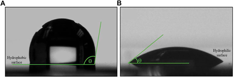
FIGURE 1. Droplet behavior on (A). a hydrophobic (before surface treatment) and (B). hydrophilic surfaces (after surface treatment).
Inkjet Printing
Inkjet printing has proved to be a rapid test and manufacturing tool especially for thin films and patterned deposition on diverse substrates (Singh et al., 2010). Inkjet system employs micron scale droplet ejection mechanism at corresponding actuation pulses utilizing nanoparticles based colloidal solution. Among the various actuation mechanisms for droplets’ ejection, piezoelectric based inkjet systems are commonly used. The operation mechanism is straight forward, and a wide range of materials can be processed at respective optimized processing parameters. Dimatix (DMP 2850) inkjet system was used for printing Ag patterns on the treated surfaces. Ag solution has the desired viscosity range i.e. ∼10 cP showing optimal jettability of the micrometer sized droplets. The process related parameters are adjusted according to the optimization steps performed beforehand. The drop-to-drop spacing was adjusted and kept at 30 µm apart, which produced uniform printed lines for both the test experiments on PI and PET substrates. Platen temperature was adjusted at 45°C, to enhance the partial evaporation of additives and surfactants added as stabilizers to the Ag solution. As a final processing step, the printed samples were kept in oven at 120°C for 2 h to completely dry the developed patterns.
Results and Discussions
Contact Angle Analyzer Analysis
Wettability of the polymeric substrates is characterized by several characteristics influencing the interfacial properties and interactions of the impacting droplets with target surfaces. These various characteristics are determined with contact angle analyser which are useful in quantifying and optimizing surface conditions for the printing related developments. Among these, the most important parameters are contact angle itself, wetting energy, spreading co-efficient and work of adhesion. Optimal values of these parameters were determined after each treatment technique. The optimal conditions (described in section Substrates Preparation) were reached based on obtaining the best possible printing results. The surface conditions producing acceptable printing results were then analysed with contact angle to determine the interfacial properties of the contacting medias. Contact angle parameters are determined before and after substrate treatments as summarised in Table 1.
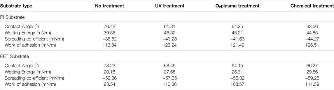
TABLE 1. Contact angle analysis on PI and PET substrates.
It is evident that the contact angle is higher both for PI and PET substrates before treatment, making it marginally hydrophobic. However, the contact angle is tuned at desired values after several trails by adjusting the UV and O2 plasma configurations. The treatment conditions were optimized (described in section Substrates Preparation) based on the printing results obtained on the substrates. The surface properties were tested at these optimally treated conditions producing best printing results. Other parameters beside the contact angle were also enhanced which significantly contributed to the printing quality of the patterns.
Printing Results on PI Using the Three Treatment Techniques
Quality of the printing results as well as high resolution patterning are at the heart of substrate treatment developments. The central idea in practicing the three different treatment techniques is to obtain the most acceptable printing results at reasonably lower and simple processing steps. These processing techniques however are adopted without compromising on the quality of the printed results and the higher resolution that could be achieved. Figure 2 shows images of the printed Ag patterns on non-treated and treated substrates. The irregularity in the print borders and non-continuous printed patterns at random are evident from Figure 2A. The repellent behavior of the surfaces due to hydrophobic properties are dominant, which causes irregular and non-uniform distribution of the ink droplets after impacting with the substrate. Even distribution and spreading of the ink with uniform edges is highly demanding especially for high resolution and dense integration of metallic structures. The minor spikes bulging out from the main printed track restricts from designing structures at much lower inter-layer spacing. For instance, maintaining a gap of few micrometers, which is ideally required for developing high resolution devices and particularly the ones comprised of interdigital electrodes. Beside this, the discontinuity in printed patterns at random spots caused by the repelling behavior of the substrate becomes more challenging. This is evident in one of the printed lines in Figure 2A. The random occurrences of such discontinuity spots make the whole development process uncertain, as a single micron-scale spot would result in dysfunctional devices, especially the metallic structures.
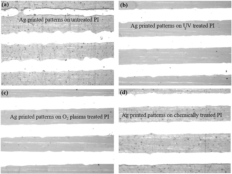
FIGURE 2. Printed Ag patterns on, (A) un-treated PI, (B). UV treated PI, (C). O2 plasma treated and (D). Chemically treated PI
To address the challenges of nonuniformity and uneven distribution of the printed droplets, the substrate surfaces are functionalized by practicing different treatment techniques. Results shown in Figures 2A–C are obtained after tuning the surface properties of the substrates. Figure 2B shows printing results of Ag patterns obtained after substrate was treated with UV (ultraviolet) light. Similarly results in Figures 2B,C are produced after treating the PI substrate with O2 plasma and chemical modification techniques, respectively. A significant improvement in the uniform distribution of droplets is achieved producing uniform edges. Comparing the results obtained with the three treatments techniques, there is no significant variation in the pattern widths as well the quality of the printed Ag lines. The results obtained with O2 plasma treatment Figure 2C have better edge uniformity, as the parameters such as O2 flow control in the chamber, power to generate plasma and finally the fine adjusting of time required to achieve the most suitable printed patterns on the substrate. On the other hand, UV plasma treatment can be controlled only through time adjustment. Nonetheless the techniques used here are compared primarily based on the results obtained and secondly on the ease in processing and reproducibility of the treatment techniques. Comparing the quality and resolution of the printing results for each corresponding treatment technique, no significant variation is observed. However, comparing the processing steps required, the chemical modification-based technique becomes attractive due to its single step process and straightforward procedure. No complex adjustments and fine tuning are required as needed in the UV as well as O2 plasma treatments.
Besides the homogenous printing on treated substrates, adhesion of the printed structures is also enhanced. This has been experimentally confirmed by performing an adhesion-loss test using a scotch tape. The printed structures both from the untreated and treated surfaces were tested. Standard cross-sectional cuts were made on the printed patterns before applying the tape. For this test, a separate large area rectangular structure was printed instead of applying the tape test on the printed line. A significant improvement in adhesion is observed for all the three treatment techniques as compared to the results on non-treated surfaces. Poor adhesion of the printed patterns with untreated substrates is observed, where more than 50% of the structure is detached. On the other hand, strong adhesion is observed after performing the tape test individually on each treated substrate samples. The minor delamination at the intersections is caused by the cuts applied while performing the standard test.
Printing on PET and Clarifoil Substrates
Further experiments were performed by validating the results on diverse substrates. The commonly practiced Polyethylene terephthalate (PET) and a cellulose based biocompatible as well as biodegradable substrates were also tested. Similar cleaning and treatment techniques were executed as were performed for PI substrate. Figures 3A,B shows printing results on untreated and treated PET substrates, respectively. Ink droplets on the untreated substrates is randomly impacted making irregular and discontinuous patterns. Ink does not spread out uniformly due to the lower spreading co-efficient and more hydrophobic properties of the surface. Wet treatment method is applied to modify the surface properties, which ultimately produced the most desirable results as shown in Figure 3B. Cellulose based substrate is also tested for the printing experiments as shown in Figures 3C,D. The untreated surface allows at least intact patterns as against untreated PET substrate, due to the absorption capability presented by the cellulose mixed in the partially plastic based contents. The spontaneous bulging out of the ink at random is controlled by the mild wet treatment technique. For the cellulose-based substrate, the wet treatment technique is slightly modified. The cleaning liquid is first sprayed on a cotton-based fabric and subsequently applied on the substrate surface for treatment. This reduces the risk to degrade the surface quality, as the solution can easily be absorbed by the cellulose content on the polymer mixture. Patterns in Figure 3D shows the results after this mild wet treatment technique. The boundaries are enhanced significantly, however the absorption capacity of the cellulose content effects largely the patterns resolution. Line width of the printed patterns are increased even after one printing cycle. This has observed to increase further with the increase in printing cycles as it is required for the enhancing the electrical conductivity. Nonetheless, this type of substrate can be applied for low resolution structures and especially for patterns requiring an inter-pattern spacing of approximately more than 200 µm. On the other hand, fine patterning and enhanced printing resolution as a result of surface treatments on PET substrate enables lower inter-patterns’ spacing that would ultimately leads to the dense integration of printed structures.
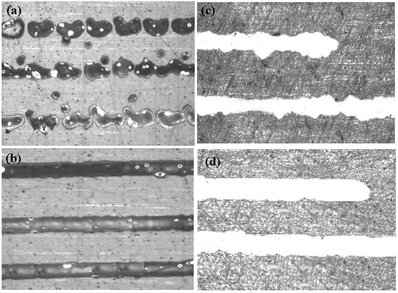
FIGURE 3. Inkjet printed results of Ag patterns on, (A) un-treated PET, (B). chemically treated PET substrate, (C). un-treated Clarifoil, (D). chemically treated Clarifoil substrate.
The comparative study performed to evaluate the optimal pattern widths and inter-pattern gaps is shown in Figures 4A–C. The wet based treatment technique is selected for this comparative study to authenticate the potentials of the newly proposed treatment technique. The gap between consecutive or neighboring printed patterns is important especially in developing sensors constituting inter digital electrodes (IDEs) and sensitive metallic structures as RTDs (resistance temperature detectors) etc. Reproducing the same printing widths as shown in all the patterns of Figures 4A–C guarantees the reliability and repeatability of the printed structures at similar treatment and printing parameters. Printed patterns’ at approximately 70 µm widths are repeatedly produced at several trials and changing the substrate as well. No significant variation in the patterns’ widths is observed albeit the multiple printing cycles for enhancing the electrical conductivity. This confirms the reliability of the proposed treatment as well as consistent printing process parameters for rapid and high throughput production of printed devices at similar conditions. The inter-digital space between the neighboring printed structures is evaluated by keeping the inter-patterns’ distance as high as 60 μm, down to 20 μm, as shown in Figures 4A–C respectively. A critical space limit of the inter-digital patterns’ i.e. 20 µm is reached as shown in Figure 4C. The minor gap in the center is still visible, however, the gap was not possible to be maintained consistently as well as not repeatably. The flow out of the ink and accumulation at the edges as a result of multiple printing cycles causes the ink to bridge the gap and making the lines interconnected. This can be avoided by increasing the platen temperature (∼60 C) for rapid and complete evaporation of the surfactants added in the ink as well as increasing the time between the subsequent printing layers. However, increasing the platen temperature to 60 °C is observed to have significant impact on the printability of the ink. Short intervals for the cleaning cycles were needed in the printing program to avoid blocking of the nozzle printhead due to the proximity and elongated exposure of the nozzle to elevated temperatures of the platen.
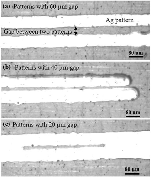
FIGURE 4. Optimizing the interdigital spacing between printed lines on a chemically treated substrate.
Temperature Sensor
A temperature sensor is developed as proof-of-concept device, a step towards realizing a wearable sensing device. Biocompatible substrates are ideally required for the development of wearable sensors and electronics. Therefore, the cellulose-based substrates used here is utilized as biocompatible substrate more suitable for wearable temperature sensors. The commonly used architecture of RTD is printed on cellulose based Clarifoil substrate. Easy fabrication through printing and subsequent fast sintering enables the rapid manufacturing of such devices on larger scale. Thickness of the selected substrate is 50 μm, which enables conformal integration to nonplanar surfaces as well as for easy manipulation and handling during the process development. Ag nanoparticles-based solution with suitable rheological properties for printing was used for all the metallic patterns as well as interconnects. The multiple printing cycles executed to achieve an acceptable electrical conductivity value simultaneously led to higher aspect ratio patterns, however the interlayer delay and moderate absorption capability of the cellulose-based substrate facilitates the higher resolution as well as minimal inter-patterns gaps. Ag pattern widths at 80 µm with gap of 60 µm between the consecutive lines were printed as RTDs repeatedly on multiple substrates. Consistency in the film quality as well as thickness of the printed lines were confirmed by characterizing the printed lines through SEM and 3D Nanoprofiler respectively as shown in Figures 5A–D. The uniformity in physical properties of the printed structures ultimately result in consistent response of the electrical and sensing responses. Figure 5A shows the optical graph of the planar as well as bent RTD structure, whereas Figure 5B shows the SEM image of the Ag surface. Surface quality and thickness of the printed line obtained from the 3D analysis (shown in Figures 5C,D respectively), it is evident that uniform thickness of about 800 nm is obtained. Some spikes are also observed, which might be due to the aggregation of the nanoparticles while deposition or uncleared dust particle. These spikes, however, can be overcome by maintaining the uniform average nanoparticles sizes in the colloidal solution as well as proper dispersion of the nanoparticles in the ink surfactants to avoid any agglomeration. Similarly, performing the printing experiments in clean room environment would help in minimizing the dust particles involvement. The most favorable conditions and materials lead to production of high aspect ratio printed structures, which produce the desired electrical conductivities, besides the physical ones. For measuring electrical resistances, a four-probe measurement tool is used to determine the resistivity. The printed thin film of Ag is recorded to have resistivity of about 20 µΩ-cm at the end of sintering step performed in a convection oven at 120°C for 1 hour, which is in acceptable ranges for such applications. Electrical measurements were performed before testing the devices on real-time wearable thermal sensing applications. Changes in the electrical resistance of the printed RTDs with temperature rise are key to the thermal analysis through such devices. Therefore, base electrical resistances were measured of the RTD structure. TCR of the RTD was calculated by keeping the sensor in a climatic chamber and recording the resistance values against the rise in temperature. Figure 6 shows the TCR graph of the printed RTD. Measuring temperature through RTDs is advantageous due to its customized sizes, simple architecture, good accuracy and highly responsive. Equation used to determine TCR of a RTD is as;
where ∆T = Tb-Ta accounts for the temperature change from base to the higher rise point, Ta is the base temperature where the sensor is checked producing 52 Ω as Ra. Tb is the successive rising temperatures and is cross-checked with the corresponding increase in resistance (Rb) as a function of temperature. Here the TCR value calculated is approximately 0.0024 K−1, which is acceptable for applications in thermal sensing.
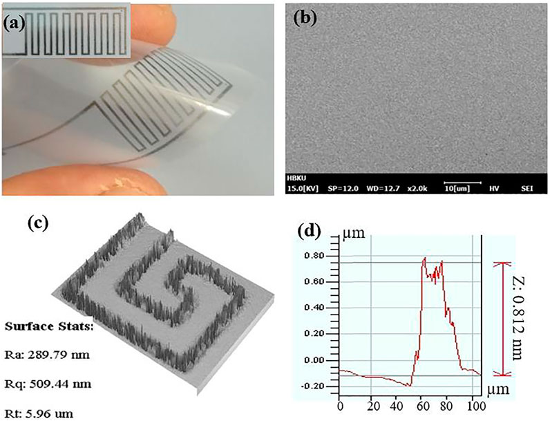
FIGURE 5. Printed results characterization (A) Optical micrograph of a printed RTD, (B). SEM image of printed Ag, 9 (C). Surface quality and roughness measured by 3D nanoprofiler, (D) thickness of a printed Ag pattern.
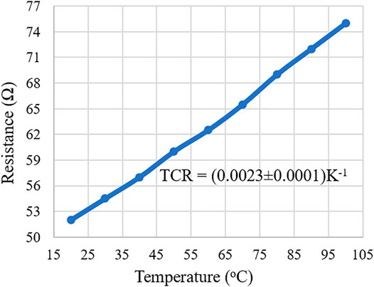
FIGURE 6. TCR of the printed RTD in a climatic chamber.
Sensor Testing
Resistance temperature detector is a contact-based temperature sensor, which changes its resistance along with the change in temperature. The energy of the atoms increases with the rise in temperature of a metallic body. Hence, the atoms vibrate and results in collision in the conduction band. These collusions result in zigzag flow of electrons and increase the overall resistance. This variation in resistance caused by temperature change is used to detect the temperature. Change in resistance is almost linear with the temperature rise. The advantages of RTD type temperature sensors are, small size, high accuracy, short response time and simple architecture. Figure 7 depicts the RTD based fabricated temperature sensor array on the biocompatible Clarifoil substrate. Left top inset of Figure 7A shows a microscopic image of a single sensor, and right top inset shows an SEM image of the printed Ag. Electrical connection was established between the measuring tool and sensor’s pad through copper connecting wires and silver epoxy paste. Sensor was tested against variable temperature from 20°C to 50°C. This range is selected due to the fact that human body temperature variations are covered within this operating window. To determine the changes, the sensor is tested to mimic the human body variation and is kept on a hotplate as shown in the inset of Figure 7B. The sensor showed change in electrical resistance from 53 to 58 Ω against temperature variation from 20°C to 50 C. The sensor response is stable and repeatable by testing multiple sensing devices. The sensor response is slightly slower at temperatures between 25-34°C, however become linear afterwards. The sensor response window is small, which can be complemented by using amplifiers circuits. The complementary circuits and filters would also help in compensating the accidental variations that might be caused from the physiological movements of the human body parts. A signal processing unit comprising amplifiers, filters and wireless communication modules will be developed for full deployment on human body.
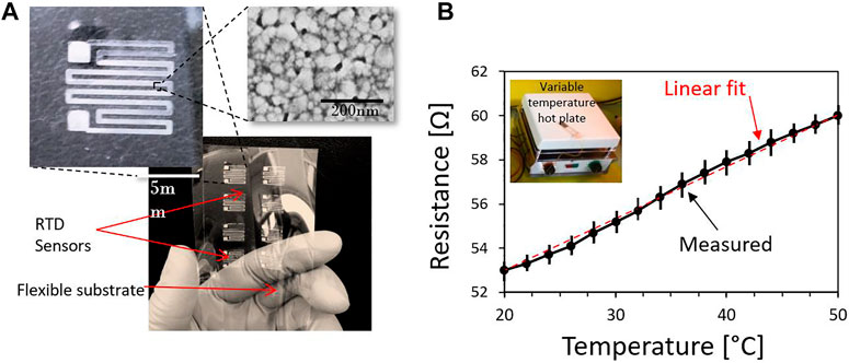
FIGURE 7. (A) Fabricated temperature sensor on PET substrate, (B) Temperature sensor measurement setup and temperature curve.
Conclusion
This research presented a comparative study based on different substrate treatment techniques and their impact on the printed results. The conventionally used UV and oxygen plasma techniques are applied along with a newly proposed chemical based rapid treatment technique. The techniques are characterized based on the processing steps and complexity, and it is concluded that newly proposed chemical based technique produces promising results considering both the surface treatment as well as printing results on it. The techniques are characterized and compared for the inkjet printing considering the quality, uniformity, and high resolution attainable at each corresponding treatment method. The three polymeric substrates used in these tests were PI, PET, and cellulose based plastic substrate. These are commonly used substrates and the cellulose-based substrate make the findings ideal for wearable related biosensing applications. A temperatures sensor is developed on the cellulose-based substrate in RTD shape using Ag ink, which is deployable on a human skin. The sensor is tested in temperature range suitable for monitoring human body thermal variations. The newly proposed chemical based treatment technique and the achieved results validate that this technique reduces the processing steps and contributes significantly to rapid manufacturing of printed sensors. Further, this rapid treatment technique is ideal for roll-to-roll manufacturing systems, where large rolls of polymeric substrates are used for fast fabrication of printed devices.
Data Availability Statement
The original contributions presented in the study are included in the article/Supplementary Materials, further inquiries can be directed to the corresponding author.
Author Contributions
All authors listed have made a substantial, direct, and intellectual contribution to the work and approved it for publication.
Funding
This work was made possible by NPRP grant NPRP11S-0104-180192 and MME01-0922-190049 from the Qatar National Research Fund (a member of Qatar Foundation). The statements made herein are solely the responsibility of the authors.
Conflict of Interest
The authors declare that the research was conducted in the absence of any commercial or financial relationships that could be construed as a potential conflict of interest.
Publisher’s Note
All claims expressed in this article are solely those of the authors and do not necessarily represent those of their affiliated organizations, or those of the publisher, the editors and the reviewers. Any product that may be evaluated in this article, or claim that may be made by its manufacturer, is not guaranteed or endorsed by the publisher.
Acknowledgments
We acknowledge the support from Qatar National research Fund for sponsoring this research.
References
Aleeva, Y., and Pignataro, B. (2014). Recent Advances in Upscalable Wet Methods and Ink Formulations for Printed Electronics. J. Mater. Chem. C 2, 6436–6453. doi:10.1039/c4tc00618f
Aydemir, C., Altay, B. N., and Akyol, M. (2021). Surface Analysis of Polymer Films for Wettability and Ink Adhesion. Color Res. Appl. 46, 489–499. doi:10.1002/col.22579
Banerjee, I., Mahapatra, S. K., Pal, C., Sharma, A. K., and Ray, A. K. (2018). Effect of Plasma Power on Reduction of Printable Graphene Oxide Thin Films on Flexible Substrates. Mater. Res. Express 5, 056405. doi:10.1088/2053-1591/aac04e
Cwikel, D., Zhao, Q., Liu, C., Su, X., and Marmur, A. (2010). Comparing Contact Angle Measurements and Surface Tension Assessments of Solid Surfaces. Langmuir 26, 15289–15294. doi:10.1021/la1020252
Haq, A. u., Boyd, A., Acheson, J., McLaughlin, J., and Meenan, B. J. (2019). Corona Discharge-Induced Functional Surfaces of Polycarbonate and Cyclic Olefins Substrates. Surf. Coat. Techn. 362, 185–190. doi:10.1016/j.surfcoat.2019.01.073
Huang, Q., and Zhu, Y. (2019). Printed Electronics: Printing Conductive Nanomaterials for Flexible and Stretchable Electronics: A Review of Materials, Processes, and Applications (Adv. Mater. Technol. 5/2019). Adv. Mater. Technol. 4, 1970029. doi:10.1002/admt.201970029
Kamyshny, A., and Magdassi, S. (2014). Conductive Nanomaterials for Printed Electronics. Small 10, 3515–3535. doi:10.1002/smll.201303000
Khan, S., Lorenzelli, L., and Dahiya, R. S. (2014). Technologies for Printing Sensors and Electronics over Large Flexible Substrates: a Review. IEEE Sensors J. 15, 3164–3185. doi:10.1109/JSEN.2014.2375203
Khan, S., Ali, S., and Bermak, A. (2019). Recent Developments in Printing Flexible and Wearable Sensing Electronics for Healthcare Applications. Sensors 19, 1230. doi:10.3390/s19051230
Khan, Y., Thielens, A., Muin, S., Ting, J., Baumbauer, C., and Arias, A. C. (2020). A New Frontier of Printed Electronics: Flexible Hybrid Electronics. Adv. Mater. 32, 1905279. doi:10.1002/adma.201905279
Kim, H., Lee, G., Becker, S., Kim, J.-S., Kim, H., and Hwang, B. (2018). Novel Patterning of Flexible and Transparent Ag Nanowire Electrodes Using Oxygen Plasma Treatment. J. Mater. Chem. C 6, 9394–9398. doi:10.1039/c8tc02377h
Malik, A., and Kandasubramanian, B. (2018). Flexible Polymeric Substrates for Electronic Applications. Polym. Rev. 58, 630–667. doi:10.1080/15583724.2018.1473424
Mäntysalo, M., Xie, L., Jonsson, F., Feng, Y., Cabezas, A. L., and Zheng, L.-R. (2012). “System Integration of Smart Packages Using Printed Electronics,” in IEEE 62nd Electronic Components and Technology Conference, 2012, San Diego, CA, USA, 29 May-1 June 2012.
Meiron, T. S., Marmur, A., and Saguy, I. S. (2004). Contact Angle Measurement on Rough Surfaces. J. Colloid Interf. Sci. 274, 637–644. doi:10.1016/j.jcis.2004.02.036
Meng, L., Zeng, T., Jin, Y., Xu, Q., and Wang, X. (2019). Surface-modified Substrates for Quantum Dot Inks in Printed Electronics. ACS omega 4, 4161–4168. doi:10.1021/acsomega.9b00195
Nemani, S. K., Annavarapu, R. K., Mohammadian, B., Raiyan, A., Heil, J., Haque, M. A., et al. (2018). Surface Modification of Polymers: Methods and Applications. Adv. Mater. Inter. 5, 1801247. doi:10.1002/admi.201801247
Palavesam, N., Marin, S., Hemmetzberger, D., Landesberger, C., Bock, K., and Kutter, C. (2018). Roll-to-Roll Processing of Film Substrates for Hybrid Integrated Flexible Electronics. Flex. Print. Electron. 3, 014002. doi:10.1088/2058-8585/aaaa04
Santidrián, A., Sanahuja, O., Villacampa, B., Diez, J. L., Benito, A. M., Maser, W. K., et al. (2019). Chemical Postdeposition Treatments to Improve the Adhesion of Carbon Nanotube Films on Plastic Substrates. ACS omega 4, 2804–2811. doi:10.1021/acsomega.8b03475
Schlisske, S., Held, M., Rödlmeier, T., Menghi, S., Fuchs, K., Ruscello, M., et al. (2018). Substrate-independent Surface Energy Tuning via Siloxane Treatment for Printed Electronics. Langmuir 34, 5964–5970. doi:10.1021/acs.langmuir.8b00304
Singh, M., Haverinen, H. M., Dhagat, P., and Jabbour, G. E. (2010). Inkjet Printing-Process and its Applications. Adv. Mater. 22, 673–685. doi:10.1002/adma.200901141
Suganuma, K. (2014). Introduction to Printed Electronics, 74. Osaka, Japan: Springer Science & Business Media.
Verkuijlen, R. O. F., Van Dongen, M. H. A., Stevens, A. A. E., Van Geldrop, J., and Bernards, J. P. C. (2014). Surface Modification of Polycarbonate and Polyethylene Naphtalate Foils by UV-Ozone Treatment and μPlasma Printing. Appl. Surf. Sci. 290, 381–387. doi:10.1016/j.apsusc.2013.11.089
Villani, F., Vacca, P., Nenna, G., Valentino, O., Burrasca, G., Fasolino, T., et al. (2009). Inkjet Printed Polymer Layer on Flexible Substrate for OLED Applications. J. Phys. Chem. C 113, 13398–13402. doi:10.1021/jp8095538
Wang, X., and Liu, J. (2016). Recent Advancements in Liquid Metal Flexible Printed Electronics: Properties, Technologies, and Applications. Micromachines 7, 206. doi:10.3390/mi7120206
Keywords: inkjet printing, polymer substrates, surface treatment, flexible electronics, wearable electronics
Citation: Khan S, Ali S, Khan A, Wang B, Al-Ansari T and Bermak A (2021) Substrate Treatment Evaluation and Their Impact on Printing Results for Wearable Electronics. Front. Electron. 2:777434. doi: 10.3389/felec.2021.777434
Received: 15 September 2021; Accepted: 06 October 2021;
Published: 16 November 2021.
Edited by:
Boyang Shen, University of Cambridge, United KingdomReviewed by:
Emilio Sardini, University of Brescia, ItalyJinghua Li, The Ohio State University, United States
Copyright © 2021 Khan, Ali, Khan, Wang, Al-Ansari and Bermak. This is an open-access article distributed under the terms of the Creative Commons Attribution License (CC BY). The use, distribution or reproduction in other forums is permitted, provided the original author(s) and the copyright owner(s) are credited and that the original publication in this journal is cited, in accordance with accepted academic practice. No use, distribution or reproduction is permitted which does not comply with these terms.
*Correspondence: Saleem Khan, c2FraGFuM0BoYmt1LmVkdS5xYQ==