 Xu Liu
 Juzhe Li
 Wei Mao
 Zhuangguang Chen1
 Hao Yu
- 1College of Microelectronics, Beijing University of Technology, Beijing, China
- 2School of Microelectronics, Southern University of Science and Technology, Shenzhen, China
This paper proposes a neural stimulator silicon chip design with an improved charge balancing technology. The proposed neural stimulation integrated circuit (IC) uses two charge balancing modules including synchronous charge detection module and short-time pulse insertion module. The synchronous charge detection module is designed based on a current splitter with ultra-small output current and an integrator circuit for neural stimulation pulse width control, which greatly reduces the residual charge remained on the electrode-tissue interface. The short-time pulse insertion module is designed based on the electrode voltage detection and compensation current control, which further reduces the accumulated residual charge and keeps the electrode voltage within a safety range of ±25 mV during multiple stimulation cycles. Finally, this neural stimulator is implemented in TSMC 0.18-μm CMOS process technology, and the chip function is tested and verified in both experiments with the electrode-tissue RC model and the PBS saline solution environment. The measurement result shows the neural stimulator chip achieves improved charge balancing with the residual charge smaller than 0.95 nC, which is the lowest compared to the traditional neural stimulator chips.
Introduction
Human machine interface is generally consist of neural stimulator chips, neural recorder chips, electrodes, sensors, RF transceiver chips, signal processors, and a computer (Bergmeister et al., 2017; Wu et al., 2018; Aman et al., 2019; Wu et al., 2019). As shown in Figure 1, the neural activities are captured by the neural recorder chips through electrodes, and the outside machines can be controlled through a signal processor and a computer. Meanwhile, the signals captured by the machines can be also sensed back to the neural stimulator chips through pressure or image sensors for closed-loop neural modulation (Bauer and Gharabaghi, 2015; Li et al., 2017; Silva, 2018; Wang et al., 2020; Seok et al., 2021). It can be found that the neural stimulator chip plays an important role in the feedback system for human-machine interface.

FIGURE 1. The block diagram of the system architecture for human-machine interface.
The main function of neural stimulator is charge delivery. According to different stimulation methods, neural stimulators can be divided into three categories, which are the voltage-controlled stimulator (VCS) (Shahrokhi et al., 2010; Haas et al., 2018; Shadmani et al., 2019; Lin and Ker, 2020), the switched-capacitor stimulator (SCS) (Lee et al., 2015; Hsu and Schmid, 2017; Lee et al., 2018), and the current-controlled stimulator (CCS) (Maghami et al., 2016; Greenwald et al., 2017; Butz et al., 2018; Chen et al., 2020). As shown in Figure 2A, a voltage-controlled stimulator can control the electrode voltage during stimulation. The electrode voltage remains constant during the stimulation pulses and shows higher power efficiency. However, the impedance of the electrode-tissue interface model is not fixed and changes with the stimulation process. Thus, the charge injected and discharged into the tissue in a single stimulation period is not equal. When the residual charge accumulates to the threshold, it may cause unpredictable damage to the nerve tissue. The structure of the switched-capacitor stimulator is shown in Figure 2B. Through the redistribution of charge on the capacitor, the residual charge in each stimulation period can be well controlled. However, the capacitance (usually hundreds of nF) in the electrode-tissue interface model is large. Besides, to complete the charge transfer successfully, the capacitance in the neural stimulation chip should also be very large, which is difficult to be integrated in the miniatured silicon chip. The current-controlled stimulator is shown in Figure 2C. In this type of stimulator, the charge injected into the tissue can be controlled by the current-mode digital-to-analog converter (DAC). The charge injection and discharge can be accurately controlled by setting the amplitude and time of the stimulator. Therefore, the current-controlled stimulator has the advantages of simple structure, small area, and easy integration, which make it become the most commonly used neural stimulator at present.
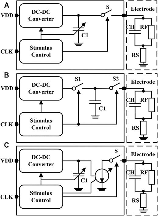
FIGURE 2. The simplified circuit of (A) the voltage-controlled stimulator (B) the switched-capacitor stimulator and (C) the current-controlled stimulator.
While the current-controlled neural stimulators also have the problem of mismatch between biphasic currents. In the traditional neural stimulator, cathodic stimulation and anodic stimulation have the same pulse width, but their amplitudes are not exactly equal due to process deviations during chip fabrication, producing a mismatch for the delivery charge. Thus, the charge injected and discharged in a single stimulation cycle is not balanced, and the electrode voltage cannot return to its initial value after each biphasic stimulation (Thurgood et al., 2009; Lee et al., 2013; Liu et al., 2018). After several cycles of stimulation, the residual charge would be accumulated and cause an electrochemical reaction on tissue-electrode interface, which is harmful for the human body (Butz et al., 2018).
Some techniques have been proposed by the researchers for solving the problem of current mismatch and charge mismatch during neural stimulation. These methods can be divided into passive charge balancing technology (Ortmanns, 2007; Xiao et al., 2008) and active charge balancing technology (Sooksood et al., 2010; Song et al., 2012; Nag et al., 2013; Greenwald et al., 2017). As shown in Figure 3A, a method called electrode shorting is used. The stimulator includes a voltage monitor and a discharge circuit, which is the most common passive charge balancing technology (Ghovanloo and Najafi, 2007; Rothermel et al., 2009). When the electrode voltage is out of the safe range, the voltage monitor control the switch S1 closed, so the electrode discharges the residual charge through the discharge circuit. The advantage of electrode shorting technology is its simple implementation. However, this kind of passive charge balancing technology requires large discharging time for residual charge removal. Besides, due to the different influences of various electrode impedance, the discharge time cannot be estimated. The stimulator with a large charge balancing time increases the period of single-cycle neural stimulation, limiting the stimulation frequency.
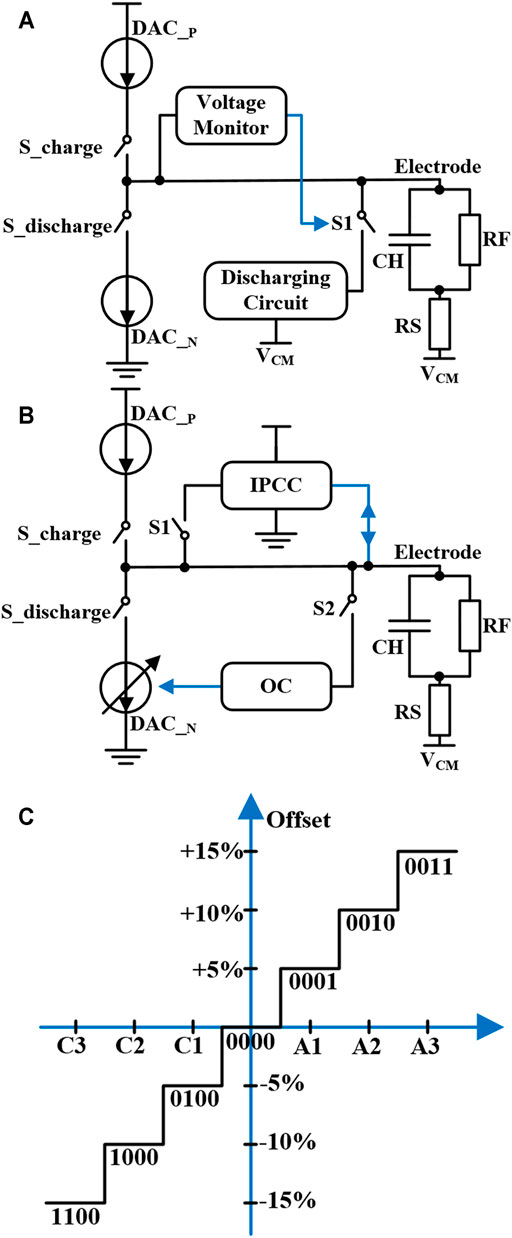
FIGURE 3. Circuit using (A) electrode shorting technology and (B) inter-pulse charge control (IPCC) and offset compensation (OC) technology. (C) The working mode using digital control technology.
An active charge balancing method is shown in Figure 3B, which combines two techniques to ensure the residual charge not damage the neural tissue under long-term stimulation (Butz et al., 2018). The first technique used is called inter-pulse charge control (IPCC), which has instantaneous compensation characteristics. When the electrode voltage exceeds a certain safe range, IPCC will compensate for the residual charge through a constant current. Another technique used is called offset compensation (OC). The feedback system controlled by proportional-integral (PI) controller compensates the cathodic stimulation current in the next stimulation pulse. These two compensation circuits work independently through switches S1 and S2, greatly improving the safety of neural stimulation. Moreover, another method uses OC based on digital control, and the working mode is shown in Figure 3C (Noorsal et al., 2012). The electrode voltage is monitored and fed back to the digital unit. The current compensation is controlled by a 4-bit digital signal to control the stimulation current amplitude change of ±15%. The minimum compensation accuracy of the system is 5% of the maximum stimulation current, and the offset state machine can only translate one bit at a time. Though this kind of active charge balancing technique has the advantage of accurate control for charge compensation, the structure of the stimulator design is complex and the accuracy also needs further improvement.
In this work, aiming to achieve the lowest residual charge, we design a charge balanced neural stimulation chip with a proposed technique which has synchronous detection of shrink current to replace the clocked pulse control in traditional neural stimulators. Moreover, short-time pulse insertion technology is used to further remove the residual charge during long-term stimulation. Our stimulator chip was taped out in TSMC 0.18-μm CMOS process technology and tested in both electrode-tissue model and PBS saline solution. The measurement result proves the reliability of the neural stimulator chip with the charge balancing method. The remaining parts of this paper are organized as follows. The second part describes the circuit implementation of our neural stimulation chip. The third part shows the measurement results of the chip based on different testing environment, and followed by a conclusion part.
Design and Implementation of the Neural Stimulator Integrated Circuit
Overall System Architecture
The overall architecture of the neural stimulator is shown in Figure 4, which is mainly composed of three parts: main DAC module, synchronous charge detection module, and short-time pulse insertion circuit. The main DAC module contains two 6-bit current-mode DACs, which generate stimulation current ranging from 8 to 504 μA. S_charge and S_discharge are the switches to control cathodic stimulation and anodic stimulation respectively. The synchronous charge detection module includes a current splitter, an integrator circuit, and a compensation circuit. The current splitter shrinks the bidirectional stimulation current produced by the main DACs and the integrator circuit combined with logic control circuits are used to perform synchronous charge detection. In order to avoid process variation induced error and possible inaccuracy caused by scaling factor mismatch of the current splitter, the compensation circuit can regulate the input current of the current splitter. The short-time pulse insertion circuit is used to guarantee the residual charge remain in a safe range after multiple stimulation cycles. When the electrode voltage is out of the safe range (Vref ± 25 mV) after the anodic stimulation pulse, a series of short-time pulses will be generated to draw the electrode voltage back to the reference voltage (Vref). To improve the safety of the neural stimulator with well charge balancing, residual charge detection circuit and short-time pulse insertion circuit are dedicatedly designed as these are the key blocks of the chip.
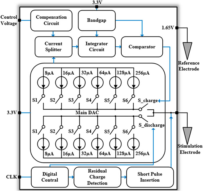
FIGURE 4. The overall system architecture of the proposed neural stimulator chip.
Synchronous Charge Detection Module
In synchronous charge detection module, the biphasic neural stimulation current are mirrored and shrunk with a certain ratio, and thus the total charge delivered to the electrode-tissue can be calculated and controlled by current integration with stimulation duration (Tan et al., 2011). Also, we use current splitter with very small current, in order to reduce the current consumption of these sub-circuits for charge detection. The current scaling ratio in the splitter circuit for current shrinking is designed as 1:104, which cannot be completed directly through the traditional current mirror. Instead, this scaling factor can be implemented by the resistance current splitter in this work, and its circuit is shown in Figure 5. In the CMOS process technology, the on-chip resistor usually has large error and takes up large chip area in fabrication. The MOS transistor working in the deep linear region can be used in this design to replace the conventional N-well resistor or other on-chip resistance devices (Bult and Geelen, 1992; Linares-Barranco and Serrano-Gotarredona, 2003; Tan et al., 2011). Taking NMOS transistor as an example, the drain source impedance in deep linear region is
As shown in Eq. 1, rds is inversely proportional to the width and length ratio (W/L) of the transistor. Shown in Figure 5A, the working process of the MOS transistor resistor (M1-M4) based current splitter can be deduced as follows. Firstly, at circuit node N1, the ratio of the current allocated to M1 and M2 is
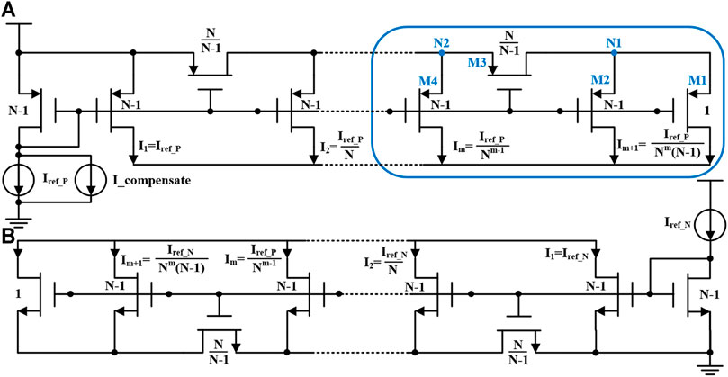
FIGURE 5. The schematic of (A) P-type current splitter and (B) N-type current splitter.
At circuit node N2, the current splitter can be expressed in resistance ratio:
It can be seen that at each shunt node, the current can be divided into two circuits with a ratio of (N-1). The initial current I1 equals to Iref_ P. The subsequent current is derived as follows.
Due to the inevitable process variation induced error, the NMOS current splitter and the PMOS current splitter cannot perfectly match the scaling factor. This mismatch error will affect the accuracy of the synchronous charge detection, which would require the charge balancing circuit to be further optimized. As such, in order to compensate for this mismatch, a compensation circuit at the current reference of the PMOS current splitter is used. The compensation circuit is controlled by an off-chip voltage with coarse and fine adjustment to realize feedback control according to the original matching offset, which improve the accuracy of the charge detection.
The schematic of the integrator circuit is shown in Figure 6A. It uses the shrinking current to synchronously detect the residual charge in the tissue (Fang et al., 2007). The circuit mainly includes an operational amplifier, six integral paths (C1-C6), a reset path (S_reset), and a comparator. The input of the integrator circuit is connected to the output of the current splitter. The six integrating paths correspond to the 6-bit switch of the DAC respectively. The switch (S_ reset) resets the initial output voltage (Vo) to VReference. The output voltage of the integrator circuit with fixed capacitance is
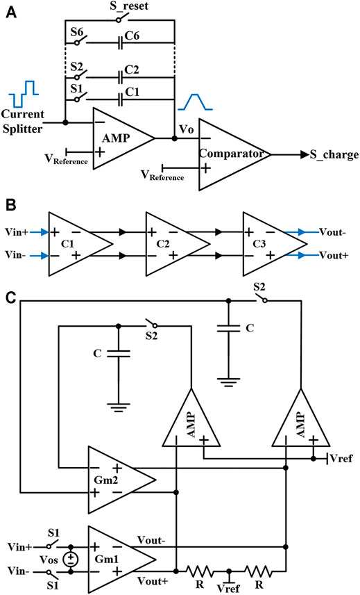
FIGURE 6. (A) The designed integrator circuit in synchronous charge detection module. (B) The circuit of the comparator based on fully differential mode. (C) Comparator with the auto-zero technology.
Cint is the fixed integrating capacitance, I is the input current of the integrator, and bitn is the control bit of the current mode DAC. The input current is controlled by bitn, which takes different integration time to reach the same output voltage. Then, the output voltage of the integrating circuit using the adjustable capacitor array is
Cref is the unit capacitance of the adjustable capacitor array. Because the input current and adjustable capacitor array are simultaneously controlled by bitn, the integration time is consistent.
In the cathodic stimulation phase, the integrator circuit inputs a negative current and the output voltage (Vo) of the operational amplifier begins to rise. At this time, the charge stored on the capacitor is the synchronous charge injected into the neural tissue. When during the anodic stimulation phase, the input of the integrator circuit changes to the forwarding current, and Vo begins to decrease until the charge on the capacitor is discharged completely. Then, the comparator state is reversed and meanwhile the anode stimulation pulse is ended, which indicates that the synchronous charge detection process is over.
The comparator circuit needs to have high-speed and high-gain performances so as to make the switch S_charge disconnect in time. In this design, three high-speed amplifiers are cascaded to form a comparator as shown in Figure 6B.
For the first-order operational amplifier, its frequency response Av (s) is
Av (0) is the DC gain of the open-loop comparator, τc = Rout ∗ CL is the time constant, so its step response Vout (s) is
Thus, the frequency response and step response of this comparator circuit are:
So the inverse Laplace transform of Eq. 10 can be obtained as shown in.
According to Eq. 11, when the total gain of the comparator is 60 dB, the supply voltage is 1.8 V, and the input voltage of the comparator is 1.8 mV, the maximum transmission delay will depend on the dominant pole of the amplifier (F = 1/τc). The detail parameters used in our design after calculation are listed in Table 1.

TABLE 1. Relationship between transmission delay and dominant pole of amplifier.
The amount of imbalanced charge caused by transmission delay (tp) of the comparator is expressed in Eq. 12.
IP is the anodic stimulation current. This imbalanced charge can also be offset by the previous compensation circuit.
Besides the transmission delay of the comparator, the offset voltage of the comparator also produce a time delay, which may account to tp in Eq. 12, so the problem of offset voltage also needs to be solved. Therefore, auto-zero technology is used in the comparator design as shown in Figure 6C, which has a calibration phase and a comparison phase in operation (Brianti et al., 1998; Danchiv and Bodea, 2008). When the self-calibration system starts to work, switch S1 is open and switch S2 is closed. At this time, the offset voltage (Vos) is sampled and stored on capacitor C. When the comparison phase starts to operate, the switch S1 is closed and the switch S2 is open. The offset voltage stored on the capacitor C generates a correction current through the transconductance amplifier GM2 to compensate the offset voltage. As a result, the input offset voltage of the comparator will be removed. The whole compensation circuit adopts the fully differential mode with a large common-mode rejection ratio, to realize a stable compensation effect.
Short-Time Pulse Insertion Circuit
The neural stimulator starts to enter the pulse insertion stage when the cathodic and anodic stimulation pulses are both over. The block diagram of the short-time pulse insertion circuit with discrimination signal generation is shown in Figure 7A. The circuit consists of three comparators, three D flip-flops, two XOR gate circuits, and a data selector. First, the TRI signal triggers the D flip-flops and stores the comparison result of the electrode voltage and the reference voltage (1.65 V). Then, the comparison results of the remaining two comparators will be stored in Q2 and Q3 sequent with the CLK. If the comparison results recorded in Q2 and Q3 are equal, it indicates that at this moment the electrode voltage is outside the safe range (the safety window is Vref ± 25mV). The data selector chooses the “1” port, and then XOR with the output of Q1 will trigger the compensation operation. If the stored voltages in Q2 and Q3 are inconsistent, it indicates that the electrode voltage is within the safe range. The data selector chooses the “0” port and turns off the compensation by XOR.
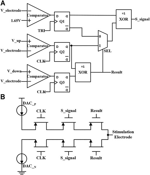
FIGURE 7. (A) The block diagram of the short-time pulse insertion circuit with discrimination signal generation. (B) The circuit of short-time pulse insertion with switches control.
The short-time pulse insertion circuit is shown in Figure 7B, which is composed of the main DACs circuit and a series of transistor switches. The circuit generates the compensation signal S_signal through the short pulse insertion discrimination mechanism described above. The compensation polarity signal (Result) and control signal (DAC_P circuit or DAC_N circuit) perform the short-time pulse insertion compensation, so the extra current will flow to the electrode-tissue interface for stimulation current compensation. When the electrode voltage returns to the safe range, the short-time pulse stops, and the compensation mechanism is turned off. As such, with the short-time pulse insertion circuit and synchronous charge detection module, the residual charge is minimized during neural stimulation.
Measurement Results
Bench-Top Measurement Results
The single-channel charge balanced neural stimulator is implemented in TSMC 180-nm CMOS process technology. The micrograph of the chip is shown in Figure 8. It includes a bandgap reference (BGR) circuit, two main DACs, two current splitters, two integrator circuits, a short-time pulse insertion circuit and logic control circuits. The total chip area is 900 μm × 840 μm.
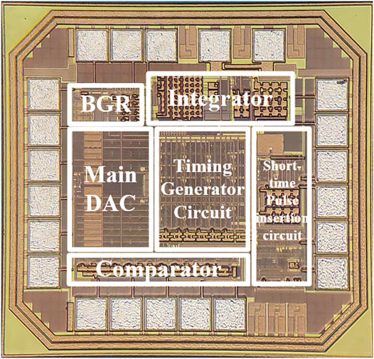
FIGURE 8. The micrograph of the neural stimulator chip.
The printed circuit board (PCB) for chip measurement includes a power module, a clock module, an implemented charge balanced neural stimulator chip, and a resistor and capacitor based tunable RC electrode-tissue model. The experiment setup for chip measurement is shown in Figure 9A. The two output port of the stimulator is connected to a load resistor (2 kΩ) on another electronic board (the white one in Figure 9A) and the reference voltage powered by a 1.65-V supply, respectively. The output current of the neural stimulator is set to 200 μA and the cathodic pulse width is set to 400 μs. Each stimulation cycle includes four stages: cathodic stimulation stage, interphase delay stage, anodic stimulation stage and short-time pulse compensation stage. The voltage waveforms captured by the oscilloscope is shown in Figure 9B. It can be seen that main function of the neural stimulator chip is validated. Figure 9C shows the waveforms when the stimulation parameters doubles (output current is set to 400 μA). It also can be seen that the pulse insertion circuit works during the interval time between each stimulation cycle. Because the insertion current of the short-time pulse circuit is small, the residual charge cannot be compensated quickly. At the end of pulse insertion, the electrode voltage returns to the reference voltage. Due to the limited resolution of ADCs in the oscilloscope for measuring, it is difficult to observe the tiny difference between the electrode voltage and reference voltage in a single cycle. But from the result showing multiple stimulation cycles, we can find that the electrode voltage keeps the value around the Vref without drifting, which means the short-time pulse insertion circuit works properly.
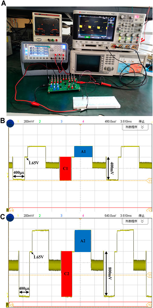
FIGURE 9. (A) The measurement setup using an on-board resistor load. (B) The electrode voltage waveform with the cathodic current of 200 μA (C) The electrode voltage waveform with the cathodic current of 400 μA.
The shaded portions in Figure 9B and Figure 9C represent the amount of charge injected and discharged to the electrode-tissue interface by the neural stimulator. The shaded area C1 and C2 represent the amount of charge injected in the cathodic stimulation stage, and A1 and A2 represent the amount of charge discharged in the anodic stimulation stage. The total charge of C1 is 80 nC (200 μA × 400 µs), and the charge of C2 is 160 nC (400 μA × 400 µs). The charge amount of A1 is 73.5 nC (105 μA × 700 µs) and A2 is 150 nC (200 μA × 750 µs). Ideally, the injected charge in cathodic stimulation phase and discharged charge in the anodic stimulation phase need to be completely same to ensure the safety of the neural stimulator. In practical, due to process-induced current mismatch and charge leakage, the residual charge has not been perfectly removed. We can see the shaded areas in Figure 9B and Figure 9C are almost matched and the residual charge before compensation is 6.5 and 10 nC, respectively, which indicates that the proposed synchronous charge detection module achieves decent charge balancing characteristics even without any compensation. If balanced positive current and negative current are generated using some matching technique, the final effect of the charge balancing will be better. Figure 10A–C show the captured voltage waveforms when the neural stimulator sets different stimulation pulse widths respectively. The clock frequency of the chip is 5 MHz and the chip can provide three optional pulse width (100, 200 and 400 µs), which meet the most application of neural stimulation.
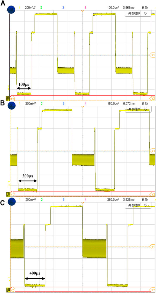
FIGURE 10. The stimulation waveforms with different cathode pulse times of (A) 100 µs, (B) 200 μs and (C) 400 µs
Figure 11A shows the measurement setup using the RC electrode-tissue model on the same PCB. We connect the output of the stimulator to the on-chip RC load and use oscilloscope to observe the voltage waveforms on the load. The first-order electrode-tissue model (CH = 200 nF, RF = 100 MΩ, RS = 8 kΩ) is adopted. The reference voltage (1.65 V) is provided by an LDO module on the PCB. The cathodic stimulation pulse width is set to 400 μs and the cathodic stimulation current amplitude is set to 104 μA. The electrode waveform displayed on the oscilloscope is shown in Figure 11B. We can see the period of single-cycle neural stimulation is 1.6 ms, including cathodic stimulation pulse width of 400 µs, an interval time of 100 μs for interphase delay, anodic stimulation pulse width of 620 µs, and short pulse insertion time of 480 μs. In order to measure the amount of the residual charge, we take a cycle of stimulation waveform for calculation. As shown in Figure 11C, the shaded parts C3 and A3 correspond to the charge amounts of cathodic stimulation and anodic stimulation respectively. Due to the load used is a first-order electrode-tissue model, the electrode voltage during the stimulation phase is continuously rising and the injected charge is accumulated on the capacitor of the load. Therefore, the method for charge calculation is to count the product of capacitance and voltage change. The area of C3 is 20 nC (200 nF × 100 mV) and the area of A3 is 24 nC (200 nF × 120 mV). The residual charge in a single cycle is only 4 nC before any compensation.
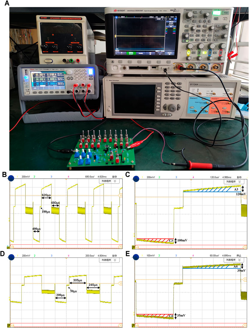
FIGURE 11. (A) The measurement setup using an electrode-tissue model on the PCB. The stimulation waveforms of the stimulator (B) with multiple stimulation cycles and (C) in a single cycle (The cathode pulse width is 400 μs and the cathodic current is 104 μA). The stimulation waveforms (D) with multiple cycles and (E) in a single cycle (The cathode pulse width is 200 μs and the cathodic current is 56 μA).
When the stimulation current is set to 56 μA and the cathodic stimulation pulse width is set to 200 µs, and the compensation circuit is also operated by fine tuning of the control voltage at this time, we can see the anodic stimulation time is reduced, as shown in Figure 11D. Now, the single neural stimulation period is 800 µs, including cathodic stimulation time of 200 µs, interphase delay time of 50 µs, anodic stimulation time of 305 µs, and short-pulse insertion time of 245 μs. Similarly, the stimulation waveform of one cycle is taken for calculation. As shown in Figure 11E, the area of the shaded part C4 is 7 nC (200 nF × 35 mV), and the area of A4 is 7.8 nC (200 nF × 39 mV). Using the compensation circuit of the neural stimulator, the residual charge in a single cycle is reduced to only 0.8 nC. The curve representing the relation between the stimulation current and measured residual charge is show in Figure 12. The residual charge can be minimized ranging from 0.63 to 0.95 nC according to different stimulation amplitudes. Even for some fragile neural stimulation, the acceptable charge value is about 15 nC/phase (Huang et al., 1999; Yigit et al., 2019).
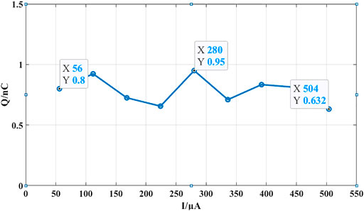
FIGURE 12. The curve representing the relation between the stimulation current and measured residual charge.
PBS Solution Experiment
To provide a similar environment of neural tissue for experiment, the phosphate buffer solution (PBS) is further used for chip measurement as the PBS osmotic pressure and ion concentration are similar to human blood. As shown in Figure 13A, two concentric needle electrodes are used and connected to the neural stimulator. One stimulating electrode is inserted into the PBS solution, the other concentric needle electrode is connected to the reference voltage (1.65 V). A power supply provides 3.3-V voltage to the chip. The oscilloscope probe is hooked on the electrode to capture its voltage waveform. The stimulation current is 104 μA and the cathodic stimulation pulse width is 100 μs. The measured voltage waveforms are shown in Figure 13B. It can be seen that the whole stimulation period is 400 µs, including cathodic stimulation time of 100 µs, interphase delay time of 25 µs, anodic stimulation time of 155 µs, and short-pulse insertion time of 120 μs.
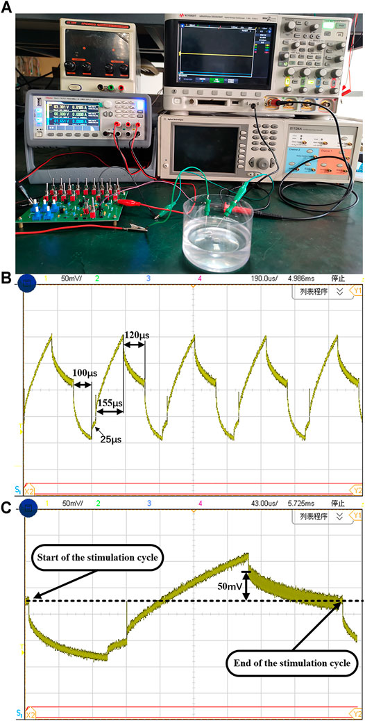
FIGURE 13. (A) The experiment setup using PBS solution. The (B) multiple cycles and (C) single cycle of electrode waveform with the cathodic current of 104 μA.
Different from the ideal first-order model presented in previous section, the characteristic impedance in PBS solution changes with the charge transfer process. Due to the inherent charge leakage of MOS switch and the possible charge leakage on other paths, the electrode voltage during the interphasic delay time does not remain to be a fix voltage value. It is a common practice to observe the voltage difference at the beginning and end of the stimulation cycle. The recognized safety range is ±50 mV (Ortmanns, 2007). The single cycle stimulation voltage waveform is shown in Figure 13C. At the end of the anodic pulse, we can observe that the residual voltage is 50 mV, which exceed the threshold of the short-time pulse circuit (±25 mV). Then the short-time pulse insertion is working to remove the residual charge in time. Comparing the beginning and end of the stimulation cycle, as shown as the dotted line in Figure 13C, the electrode voltage remains the same. As shown in Figure 13B, the electrode voltage can return to the reference voltage at the end of each stimulation cycle, which ensure the correct operation of the neural stimulator in the next cycle. Based on the test environment of PBS solution, the function and effectiveness of this design are verified, and ensure the safety of neural stimulator. Table 2 shows the comparison between this work and other articles. It can be seen from the table that our chip has advantage in smaller area and lower maximum residual charge based on synchronous charge detection and short-time pulse insertion technology.
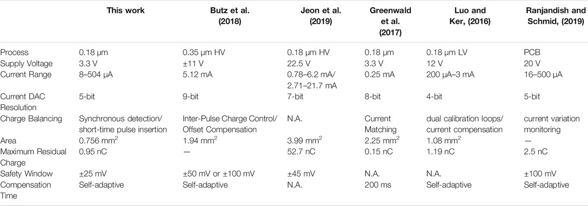
TABLE 2. The comparison between this work and other articles.
Conclusion
A charge balanced neural stimulator IC is proposed, implemented, and tested in this work. Two key modules using different charge balancing technologies have been designed in the chip to achieve the minimum residual charge and ensure the safety of neural stimulation. The synchronous charge detection module composed of a current splitter and integrator circuit with current compensation reduces the residual charge to less than 0.95 nC. Moreover, the short-time pulse insertion circuit further improves the charge balancing during long-term neural stimulation. The neural stimulator chip was tested in both electrode-tissue RC model and PBS solution. The measurement results show that the stimulator has a reliable charge balancing feature in neural stimulation. This charge balanced neural stimulator could be used in the human-machine interface with feedback function.
Data Availability Statement
The original contributions presented in the study are included in the article/Supplementary Material, further inquiries can be directed to the corresponding author.
Author Contributions
XL, JL, and ZC: analysis and design of the integrated circuits. PW and ZC: simulation of the circuits and layout check. XL, JL, WM and HY: parameters analysis and writing and revising of the article. All authors contributed to the article and approved the submitted version.
Funding
This work is supported by the National Natural Science Foundation of China (Grant No. 61806012), the National Natural Science Foundation of China (NSFC) (Key Program Grant No. 6203000189), the Innovative Team Program of Education Department of Guangdong Province (Grant No. 2018KCXTD028), the Shenzhen Science and Technology Program (Grant No. KQTD2020020113051096) and the Key-Area Research and Development Program of Guangdong Province (Grant No. 2019B010142001).
Conflict of Interest
The authors declare that the research was conducted in the absence of any commercial or financial relationships that could be construed as a potential conflict of interest.
Publisher’s Note
All claims expressed in this article are solely those of the authors and do not necessarily represent those of their affiliated organizations, or those of the publisher, the editors and the reviewers. Any product that may be evaluated in this article, or claim that may be made by its manufacturer, is not guaranteed or endorsed by the publisher.
References
Aman, M., Bergmeister, K. D., Festin, C., Sporer, M. E., Russold, M. F., Gstoettner, C., et al. (2019). Experimental Testing of Bionic Peripheral Nerve and Muscle Interfaces: Animal Model Considerations. Front. Neurosci. 13, 1442. doi:10.3389/fnins.2019.01442
Bauer, R., and Gharabaghi, A. (2015). Reinforcement Learning for Adaptive Threshold Control of Restorative Brain-Computer Interfaces: a Bayesian Simulation. Front. Neurosci. 9, 36. doi:10.3389/fnins.2015.00036
Bergmeister, K. D., Vujaklija, I., Muceli, S., Sturma, A., Hruby, L. A., Prahm, C., et al. (2017). Broadband Prosthetic Interfaces: Combining Nerve Transfers and Implantable Multichannel EMG Technology to Decode Spinal Motor Neuron Activity. Front. Neurosci. 11, 421. doi:10.3389/fnins.2017.00421
Brianti, F., Manstretta, A., and Torelli, G. (1998). High-speed Autozeroed CMOS Comparator for Multistep A/D Conversion. Microelectronics J. 29, 845–853. doi:10.1016/s0026-2692(97)00123-7
Bult, K., and Geelen, G. J. G. M. (1992). An Inherently Linear and Compact MOST-Only Current Division Technique. IEEE J. Solid-state Circuits 27, 1730–1735. doi:10.1109/4.173099
Butz, N., Taschwer, A., Nessler, S., Manoli, Y., and Kuhl, M. (2018). A 22 V Compliant 56 μ W Twin-Track Active Charge Balancing Enabling 100% Charge Compensation Even in Monophasic and 36% Amplitude Correction in Biphasic Neural Stimulators. IEEE J. Solid-State Circuits 53, 2298–2310.
Chen, Z., Liu, X., and Wang, Z. (2020). A Charge Balancing Technique for Neurostimulators. Analog Integr. Circ. Sig Process. 105, 483–496. doi:10.1007/s10470-020-01726-6
Danchiv, A., and Bodea, M. (2008). "Residual Offset Optimization for a Continuous Time Autozero Amplifier", in: 2008 International Conference on Signals and Electronic Systems. Krakow, Poland, Sept 2008. doi:10.1109/icses.2008.4673415
Fang, X., Wills, J., Granacki, J., Lacoss, J., Arakelian, A., and Weiland, J. (2007). "Novel Charge-Metering Stimulus Amplifier for Biomimetic Implantable Prosthesis", in:2007 IEEE International Symposium on Circuits and Systems, New Orleans, LA, USA, May 2007. doi:10.1109/iscas.2007.378801
Ghovanloo, M., and Najafi, K. (2007). A Wireless Implantable Multichannel Microstimulating System-On-A-Chip with Modular Architecture. IEEE Trans. Neural Syst. Rehabil. Eng. 15, 449–457. doi:10.1109/tnsre.2007.903970
Greenwald, E., Maier, C., Wang, Q., Beaulieu, R., Etienne-Cummings, R., Cauwenberghs, G., et al. (2017). A CMOS Current Steering Neurostimulation Array with Integrated DAC Calibration and Charge Balancing. IEEE Trans. Biomed. Circuits Syst. 11, 324–335. doi:10.1109/tbcas.2016.2609854
Haas, M., Vogelmann, P., and Ortmanns, M. (2018). A Neuromodulator Frontend with Reconfigurable Class-B Current and Voltage Controlled Stimulator. IEEE Solid-state Circuits Lett. 1, 54–57. doi:10.1109/lssc.2018.2827885
Hsu, W.-Y., and Schmid, A. (2017). Compact, Energy-Efficient High-Frequency Switched Capacitor Neural Stimulator with Active Charge Balancing. IEEE Trans. Biomed. Circuits Syst. 11, 878–888. doi:10.1109/tbcas.2017.2694144
Huang, C. Q., Shepherd, R. K., Center, P. M., Seligman, P. M., and Tabor, B. (1999). Electrical Stimulation of the Auditory Nerve: Direct Current Measurement In Vivo. IEEE Trans. Biomed. Eng. 46, 461–469. doi:10.1109/10.752943
Jeon, Y.-J., Yao, L., Gao, Y., and Arasu, M. A. (2019). A 0.034% Charge-Imbalanced Neural Stimulation Front-End (SFE) IC with On-Chip Voltage Compliance Monitoring Circuit and Analysis on Resting Potential by Utilizing the SFE IC. IEEE Trans. Circuits Syst. Regular Pap. 66, 3797–3810.
Kiseok Song, K., Hyungwoo Lee, H., Sunjoo Hong, S., Hyunwoo Cho, H., Unsoo Ha, U., and Hoi-Jun Yoo, H. J. (2012). A Sub-10 nA DC-balanced Adaptive Stimulator IC with Multi-Modal Sensor for Compact Electro-Acupuncture Stimulation. IEEE Trans. Biomed. Circuits Syst. 6, 533–541. doi:10.1109/tbcas.2012.2232292
Lee, H.-M., Kwon, K. Y., Li, W., and Ghovanloo, M. (2015). A Power-Efficient Switched-Capacitor Stimulating System for Electrical/Optical Deep Brain Stimulation. IEEE J. Solid-state Circuits 50, 360–374. doi:10.1109/jssc.2014.2355814
Lee, H.-M., Park, H., and Ghovanloo, M. (2013). A Power-Efficient Wireless System with Adaptive Supply Control for Deep Brain Stimulation. IEEE J. Solid-state Circuits 48, 2203–2216. doi:10.1109/jssc.2013.2266862
Lee, H. M., Howell, B., Grill, W. M., and Ghovanloo, M. (2018). Stimulation Efficiency with Decaying Exponential Waveforms in a Wirelessly Powered Switched-Capacitor Discharge Stimulation System. IEEE Trans. Biomed. Eng. 65, 1095–1106. doi:10.1109/TBME.2017.2741107
Li, L., Xu, G., Zhang, F., Xie, J., and Li, M. (2017). Relevant Feature Integration and Extraction for Single-Trial Motor Imagery Classification. Front. Neurosci. 11, 371. doi:10.3389/fnins.2017.00371
Lin, S.-P., and Ker, M.-D. (2020). Design of Stage-Selective Negative Voltage Generator to Improve On-Chip Power Conversion Efficiency for Neuron Stimulation. IEEE Trans. Circuits Syst. 67, 4122–4131. doi:10.1109/tcsi.2020.3012086
LinaresBarranco, B., and SerranoGotarredona, T. (2003). On the Design and Characterization of Femtoampere Current-Mode Circuits. IEEE J. Solid-state Circuits 38, 1353–1363. doi:10.1109/jssc.2003.814415
Liu, X., Yao, L., Ng, K. A., Li, P., Wang, W., Je, M., et al. (2018). A Power-Efficient Current-Mode Neural/muscular Stimulator Design for Peripheral Nerve Prosthesis. Int. J. Circ. Theor. Appl. 46, 692–706. doi:10.1002/cta.2434
Luo, Z., and Ker, M.-D. (2016). A High-Voltage-Tolerant and Precise Charge-Balanced Neuro-Stimulator in Low Voltage CMOS Process. IEEE Trans. Biomed. Circuits Syst. 10, 1087–1099. doi:10.1109/tbcas.2015.2512443
Maghami, M. H., Sodagar, A. M., and Sawan, M. (2016). Versatile Stimulation Back-End with Programmable Exponential Current Pulse Shapes for a Retinal Visual Prosthesis. IEEE Trans. Neural Syst. Rehabil. Eng. 24, 1243–1253. doi:10.1109/tnsre.2016.2542112
Nag, S., Xiaofeng Jia, X., Thakor, N., and Sharma, D. (2013). Flexible Charge Balanced Stimulator with 5.6 fC Accuracy for 140 nC Injections. IEEE Trans. Biomed. Circuits Syst. 7, 266–275. doi:10.1109/tbcas.2012.2205574
Noorsal, E., Sooksood, K., Xu, H., Hornig, R., Becker, J., and Ortmanns, M. (2012). A Neural Stimulator Frontend with High-Voltage Compliance and Programmable Pulse Shape for Epiretinal Implants. IEEE J. Solid-state Circuits 47, 244–256. doi:10.1109/jssc.2011.2164667
Ortmanns, M. (2007). "Charge Balancing in Functional Electrical Stimulators: A Comparative Study", in: 2007 IEEE International Symposium on Circuits and Systems, New Orleans, LA, USA, May 2007. doi:10.1109/iscas.2007.378802
Ranjandish, R., and Schmid, A. (2019). A Design Methodology for Charge-Balanced Stimulators Based on Anodic Current Variation Monitoring. Analog Integr. Circ. Sig Process. 101, 341–350. doi:10.1007/s10470-019-01462-6
Rothermel, A., Liu, L., Aryan, N. P., Fischer, M., Wuenschmann, J., Kibbel, S., et al. (2009). A CMOS Chip with Active Pixel Array and Specific Test Features for Subretinal Implantation. IEEE J. Solid-state Circuits 44, 290–300. doi:10.1109/jssc.2008.2007436
Seok, D., Lee, S., Kim, M., Cho, J., and Kim, C. (2021). Motion Artifact Removal Techniques for Wearable EEG and PPG Sensor Systems. Front. Elect. 2. doi:10.3389/felec.2021.685513
Shadmani, A., Viswam, V., Chen, Y., Bounik, R., Dragas, J., Radivojevic, M., et al. (2019). Stimulation and Artifact-Suppression Techniques for In Vitro High-Density Microelectrode Array Systems. IEEE Trans. Biomed. Eng. 66, 2481–2490. doi:10.1109/tbme.2018.2890530
Shahrokhi, F., Abdelhalim, K., Serletis, D., Carlen, P. L., and Genov, R. (2010). The 128-channel Fully Differential Digital Integrated Neural Recording and Stimulation Interface. IEEE Trans. Biomed. Circuits Syst. 4, 149–161. doi:10.1109/tbcas.2010.2041350
Silva, G. A. (2018). A New Frontier: The Convergence of Nanotechnology, Brain Machine Interfaces, and Artificial Intelligence. Front. Neurosci. 12, 843. doi:10.3389/fnins.2018.00843
Sooksood, K., Stieglitz, T., and Ortmanns, M. (2010). An Active Approach for Charge Balancing in Functional Electrical Stimulation. IEEE Trans. Biomed. Circuits Syst. 4, 162–170. doi:10.1109/tbcas.2010.2040277
Tan, J. Y. J., Liu, X., Wee, K. H., Yen, S.-C., and Xu, Y. P. (2011). "A Programmable Muscle Stimulator Based on Dual-Slope Charge Balance", in: IEEE Asian Solid-State Circuits Conference 2011, Jeju,South Korea. Nov 2011. doi:10.1109/asscc.2011.6123636
Thurgood, B. K., Warren, D. J., Ledbetter, N. M., Clark, G. A., and Harrison, R. R. (2009). A Wireless Integrated Circuit for 100-channel Charge-Balanced Neural Stimulation. IEEE Trans. Biomed. Circuits Syst. 3, 405–414. doi:10.1109/tbcas.2009.2032268
Wang, H., Su, Q., Yan, Z., Lu, F., Zhao, Q., Liu, Z., et al. (2020). Rehabilitation Treatment of Motor Dysfunction Patients Based on Deep Learning Brain-Computer Interface Technology. Front. Neurosci. 14, 595084. doi:10.3389/fnins.2020.595084
Wu, Y., Jiang, D., Bardill, A., Bayford, R., and Demosthenous, A. (2019). A 122 Fps, 1 MHz Bandwidth Multi-Frequency Wearable EIT Belt Featuring Novel Active Electrode Architecture for Neonatal Thorax Vital Sign Monitoring. IEEE Trans. Biomed. Circuits Syst. 13, 927–937. doi:10.1109/tbcas.2019.2925713
Wu, Y., Jiang, D., Liu, X., Bayford, R., and Demosthenous, A. (2018). A Human-Machine Interface Using Electrical Impedance Tomography for Hand Prosthesis Control. IEEE Trans. Biomed. Circuits Syst. 12, 1322–1333. doi:10.1109/tbcas.2018.2878395
Xiao Liu, L., Demosthenous, A., and Donaldson, N. (2008). An Integrated Implantable Stimulator that Is Fail-Safe without Off-Chip Blocking-Capacitors. IEEE Trans. Biomed. Circuits Syst. 2, 231–244. doi:10.1109/TBCAS.2008.2003199
Keywords: neural stimulation, active charge balancing, synchronous charge detection, residual charge, electrode-tissue model
Citation: Liu X, Li J, Mao W, Chen Z, Chen Z, Wan P and Yu H (2021) A Charge Balanced Neural Stimulator Silicon Chip for Human-Machine Interface. Front. Electron. 2:773812. doi: 10.3389/felec.2021.773812
Received: 10 September 2021; Accepted: 07 October 2021;
Published: 22 October 2021.
Edited by:
Yu Wu, University College London, United KingdomReviewed by:
Qiuyang Lin, Interuniversity Microelectronics Centre (IMEC), BelgiumJiajie Huang, Shanghai Jiao Tong University, China
Copyright © 2021 Liu, Li, Mao, Chen, Chen, Wan and Yu. This is an open-access article distributed under the terms of the Creative Commons Attribution License (CC BY). The use, distribution or reproduction in other forums is permitted, provided the original author(s) and the copyright owner(s) are credited and that the original publication in this journal is cited, in accordance with accepted academic practice. No use, distribution or reproduction is permitted which does not comply with these terms.
*Correspondence: Hao Yu, eXVoM0BzdXN0ZWNoLmVkdS5jbg==