 H. Esmaeili Taheri1
 Simon Rondeau-Gagné
- 1Department of Electrical and Computer Engineering, Center for Engineering and Innovation (CEI), University of Windsor, Windsor, ON, Canada
- 2Department of Chemistry and Biochemistry, Advanced Materials Centre of Research (AMCORe), University of Windsor, Windsor, ON, Canada
Organic field-effect transistors (OFETs) are at the forefront of next generation electronics. This class of devices is particularly promising due to the possibility of fabrication on mechanically compliant and conformable substrates, and potential manufacturing at large scale through solution deposition techniques. However, their integration in circuits, especially using stretchable materials, is still challenging. In this work, the design and implementation of a novel structure for an integrated CMOS readout circuitry is presented and its fundamentals of operation are provided. Critical for sensing applications, the readout circuitry described is highly linear. Moreover, as several sources of mismatch and error are present in CMOS and OFET devices, a calibration technique is used to cancel out all the mismatches, thus delivering a reliable output. The readout circuit is verified in TSMC 0.18 μm CMOS technology. The maximum total power consumption in the proposed readout circuit is less than 571 μW, while fully loaded calibration circuit consumes a power less than 153 μW, making it suitable for sensors applications. Based on previously reported high mobility and stretchable semiconducting polymers, this new design and readout circuitry is an important step toward a broader utilization of OFETs and the design of stretchable sensors.
Introduction
Microelectronic systems have changed many aspects of human life. They have revolutionized data processing and telecommunications in volume and speed, which have provided solutions for complicated issues. Particularly in the age of the Internet of Things (IoT), new and emerging microelectronic are constantly developed, which include flexible monitors, health and environmental monitoring systems and artificial skin for robotics. These new devices not only revolutionize contemporary technologies, but also request additional functionalities that challenge electronic engineers and materials scientists. (Murmann and Xiong, 2010). Among other, smart and conformable sensors are particularly challenging to design and fabricate. (Senthamizhan et al., 2019). A smart sensor should be capable of being exposed to the target analyte(s), sensing it, producing a proportional signal, and measuring and amplifying it. (Uslu et al., 2004; Gonçalves et al., 2008; Velliste et al., 2008; Asplund et al., 2010; Rivnay et al., 2014; Bhalla et al., 2017). Furthermore, next generation electronics and sensors will not only need to be electrically reliable and performant but will also need to be implemented on different objects and shapes. (Gubbi et al., 2013; Zhan et al., 2014). Among the different types of electronics to generate and achieve smart sensors, organic field-effect transistors (OFETs) are particularly promising given their chemical versatility, sensitivity and the possibility of being implemented on conformable or stretchable matrices. (Rogers and Bao, 2002; Sirringhaus, 2014). One of the most important fields of application for OFETs is point-of-care (PoC) systems, in which the test system should be exposed to health indicator analytes. The result of this exposure is a signal, which is amplified and transmitted to a digital processing unit, in which, appropriate responses are produced. (Torsi et al., 2013). These systems should be developed taking into consideration that most users are inexperienced and non-professional individuals. Therefore, the system should be simple and user-friendly. In addition, PoC systems are most helpful when they can process different health indicators in a single smart sensing unit, preferably installed directly on the human body or sensing environment conformably. (Hammock et al., 2013; Torsi et al., 2013).
π-Conjugated semiconducting polymers have been attracting a lot of attention for the design and fabrication of these next generation electronics, mostly due to their good mechanical properties (low Young’s moduli and good strain resistance), crucial to access body-conformable devices and skin-inspired electronics. (Zhao et al., 2015; Wen et al., 2017; Xu et al., 2017). This is a critical advantage, as the more intimate the contact between these devices and the surfaces from which these signals originate, the more optimal and sensitive the sensing capabilities. (Su et al., 2015; Bae et al., 2016). Strategies for achieving organic materials with molecular stretchability and skin-mimicking properties have been summarized comprehensively in previous reports. (Ocheje et al., 2017). In recent years, our group and others reported the synthesis of molecularly stretchable and mechanically robust semiconducting polymers with charge transport properties close to that of amorphous silicon. (Mei and Bao, 2014; Oh et al., 2016; Wu et al., 2016; Ocheje et al., 2018). These new mechanically robust materials are particularly promising as active layer in sensors using substrates such as plastic and can be suitable for applications such as health monitoring, environmental monitoring, flexible displays, artificial skins, and radio frequency identification (RFID). (Baude et al., 2003; Someya et al., 2004; Kato et al., 2007; Feng et al., 2016; Frick et al., 2016; Tang et al., 2016; Li et al., 2018).
The push for OFET-based CMOS readout circuits is driven by the desire for devices with lower power consumption, lower cost, that can be miniaturized; all the while being compatible with existing electronic systems and thereby allowing for seamless integration. (Lei et al., 2016). Although organic materials have been investigated vastly and their functionality is proven in smart sensor applications, the design of an effective readout circuit for biosensors fabricated from organic thin film transistors, required to convert the output of the OFET to appropriate format for the digital backbone processing unit, has remained an important challenge for various reasons. First, designing readout circuitry for integration with OFETs often requires high voltages and produces very small currents in response to the analyte variations. This can partially explain why the OFET readout circuits are still quite rare in the literature, and why OFETs are often used in discrete circuits. The power consumption is also another parameter often challenging to control. Finally, the utilization of n-type organic semiconductors is still underexploited in the literature due to their relative low stability compare to their p-type counterparts.
To tackle these challenges, different circuit readouts for OFET-based sensors have been proposed recently. Among others, Li et al. reported a readout circuit for a low voltage OFET used for pH sensing. (Li et al., 2018). The proposed readout circuit takes the drain current of the OFET and delivers VDD and Vref. The trans-impedance amplifier (TIA) converts the drain current to a voltage and the programmable gain amplifier (PGA) adjusts the dynamic range of the sensor. Ultimately, the processed data is transmitted to a smart phone for display. A second approach towards implementation of CMOS readout circuit for OFET based sensors, has been proposed by Feng et al. (2016) where a readout circuit implemented on PCB is proposed. Interestingly, the sensor was shown to be able to detect NH3 concentrations of 5–25 ppm. Other examples of new readouts circuitry for OFET-based sensors have also been proposed for sensing different analytes, such as ethanol. (Frick et al., 2016). Despite being efficient, these sensors require high power supply along with high-power consumption. This significantly limits their utilization for low-power, portable PoC applications, which are usually powered by battery, and face serious power constraints. Therefore, the challenge that limits the design of an integrated readout circuit for low voltage OFET based sensors remains.
Herein, we report a new approach for OFET integration and implementation toward a conformable circuitry based on computational simulation and in silico modelling. This theoretical and computation approach for circuit design presents important advantages, including the possibility to modify and fine-tune multiple parameters of the circuitry. The fabrication of OFET requires various challenging steps, and the design of high mobility n-type materials is still challenging. Therefore, the utilization of computer simulation is a particularly efficient approach to design novel circuitry, especially for biosensor devices based on thin film transistors. In this work, a universal readout circuitry was designed to address important obstacles in OFET-based sensor implementation. The new readout circuit was found to be able to detect very small variations in the drain current of the OFET, as low as 100 nA, in three different phases. While the reset phase does not consume significant power, the calibration and exposure phases consume almost all of the required power from the 1.8 V power supply in 0.18 µm CMOS technology. In fact, the highest power consumed by the readout circuit is 571 μW, which is significantly lower than other proposed readout based on these organic electronics. The proposed readout structure is not only a promising candidate for low-power, portable sensing applications, but the new computational simulation approach used in this work represent an important tool for the fabrication of new advanced and functional electronics.
Results and Discussion
Organic materials, particular π-conjugated polymers, have important advantages over inorganic semiconductors, including low cost and high throughput fabrication enabled through solution deposition. Organic semiconductors also have low elastic modulus, particularly interesting for the fabrication of skin-inspired stretchable and conformable devices. These unique features have resulted in the significant growth-rate of the use of organic materials in health care applications such as organic thin-film transistors (OTFTs) for biological marker detection, drug delivery, and neural recording and stimulation. (Adhikari and Majumdar, 2004; Isaksson et al., 2007; O'Connor et al., 2015; Schwartz et al., 2013; Irimia-Vladu, 2014; Liao et al., 2015). In these novel biosensors based on OFETs, the readout circuitry, required to monitor the output of the biosensor, is typically implemented using conventional CMOS technology. Therefore, the integration of OFET with the CMOS circuit is highly desirable.
There are three main characteristics that are important for OFET integration. In CMOS technology, the maximum available voltage supply is limited, so the OFET should be able to work within these restrictions. Secondly, the small drain current of the OFET is another issue which means the CMOS circuit should be able to sense low current values and be able to amplify these currents. Since sensor linearity is one important characteristic, this amplification should be done in a linear manner. (Torsi et al., 2013). Finally, the drain current of the OFET experiences small variations during analyte exposure. Therefore, the CMOS integrated readout circuit should be able to sense low current variations on small biased drain currents. As shown in Table 1, an OFET, which can work with voltages in the range of (0 to 1.8 V) will deliver drain currents lower than 1 μA. Recently, Yan et al. evaluated OFETs in several sensing applications and it can be inferred that in different applications, the drain current experiences variations in the range of (0.9*IDbl,1*IDbl) where IDbl is the base line drain current of the OFET at the operating point. This means that the integrated readout circuit should be able to provide the above mentioned voltage range and should sense currents as low as 0.1 μA. It is also important to note that most materials used for sensing application are p-type semiconductors. The design of OFET-based circuit readout from n-type materials is highly desirable to complement the current technology. In order to use PMOS transistors for the readout circuit, due to their better noise performance, we designed the proposed readout circuit using a n-type OFET. However, it is important to note that the circuits can be altered to be employed in p-type OFET sensing structures.
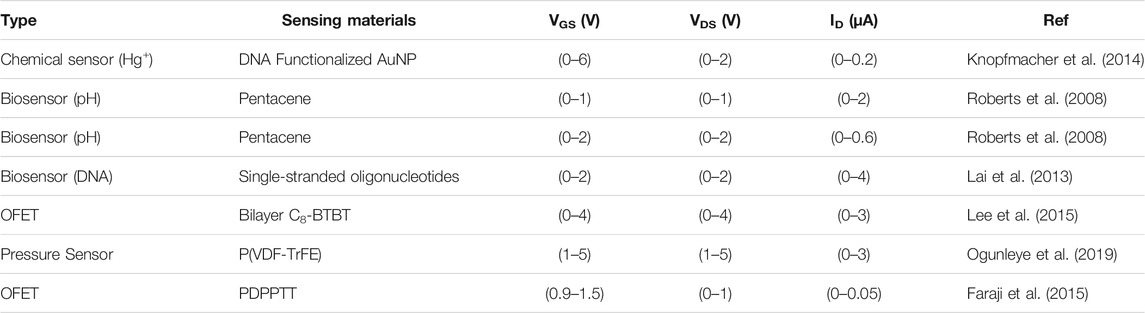
TABLE 1. Operating voltages and output current range of recently reported low voltage OFETs.
In a biosensor, the drain current of the OFET will fluctuate with analyte exposure. Given that the concentration of the analyte can be particularly low, the drain current variations can be small and difficult to detect. (Lai et al., 2013). To address this challenge, the sensing circuit has to be sensitive to small current variation and able to linearly amplify these variations. In our computational simulation, amplification of the output current is performed by using a linear current amplifier integrated on a simple integrator. Since the variations of the drain current of the OFET are essential, our simulations use two OFETs to sense and amplify the current variations due to analyte exposure. The current amplifier used in our computational analysis is shown in Figure 1, and it is important to mention that the nature of the analyte was kept broad given that multiple and diverse analytes can be selected. The amplifier is composed of two main branches. One branch is derived with a “sensing OFET”, which is exposed to the analyte. The other is derived with an OFET which is called the “reference OFET” and is not exposed to the target analyte. The bias conditions of the two OFETs are identical. Since two OFETs are identical and their bias conditions are the same, any difference in drain currents of the OFETs will arise from analyte exposure. The drain currents of the sensing OFET and reference OFET are amplified in cascode current mirrors of M1-4 and M5-8, respectively. The reference OFET drain current is mirrored in M9, 10 and is subtracted from the amplified sensing OFET drain current in node “X”. This configuration of current amplification has a unique advantage. Regarding the operating region of M9, the drain currents of the sensing and the reference OFETs feed M2,5, respectively. These two transistors supply the drain current of the M4,7 which in turn drive M3,8. The current which is drown from the drain of M8 biases the M9 transistor in active region. The current mirror ratios in Figure 2 for the two cascode current mirrors are 348, while the mirror ratio for the M9,10 is equal to unity, to subtract the current of the sensing and the reference OFETs.
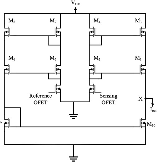
FIGURE 1. Schematic of the proposed linear current amplifier based on OFET device.
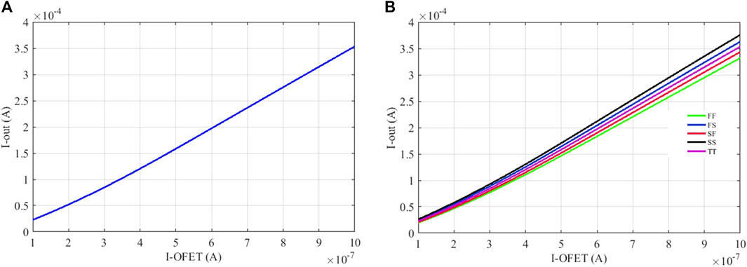
FIGURE 2. Iout-IOFET graph illustrating characteristic of current amplifiers (A), and Iout-IOFET characteristic of current amplifier in different corner cases (B). The four case scenarios in which the NMOS and PMOS transistors show the extreme speeds are considered as FF (Fast NMOS, Fast PMOS), FS (Fast NMOS, Slow PMOS), SF (Slow NMOS, Fast PMOS), and SS (Slow NMOS, Slow PMOS). These four corner situations are usually compared with typical situation (TT), where both NMOS and PMOS transistors are working at typical speed.
One of the main problems in organic transistors is that they show significant hysteresis effect. It means that, during time and with each cycle of operation, their I-V characteristic will change. The current amplification scheme that is used here, applies two identical OFETs which their drain currents experience similar variations. This configuration along with the calibration technique that is discussed later, will result in an almost hysteresis free sensor. The new current amplifier amplifies currents between 100 nA and 1 uA with an almost fixed gain of 350. The characteristic of this current amplifier is shown in Figure 2. The operation of the circuit was evaluated computationally under different process, voltage and temperature (PVT) situations. As shown in Figure 2, the four worst case scenarios in which the NMOS and PMOS transistors show the extreme speeds are considered as FF (Fast NMOS, Fast PMOS), FS (Fast NMOS, Slow PMOS), SF (Slow NMOS, Fast PMOS), and SS (Slow NMOS, Slow PMOS). These four corner situations are compared with typical situation (TT), where both NMOS and PMOS transistors are working at typical speed. The right sub-figure in Figure 2 shows the performance of the circuit in typical situation (TT), and the four other corner cases along with the typical situation are shown in the left sub-figure. From the results obtained, we can conclude that this design does not suffer from PVT variations. Therefore, this current amplifier has good performance in different corner case situations, and the gain of the amplifier experiences small changes and the linearity is retained.
The largest tensile deformations experienced on the human body are approximately 30% elongation, meaning that conformable devices laminated on the body can experience geometry changes of similar magnitude. Device performance and the measured current are highly dependent on the channel length and width and retaining these are crucial to maintain the fidelity of a chemical sensor. Any drop in current that is not due to the sensing of a target analyte could render false results. Consequently, the ability to apply increasing voltage in response to a strain-induced reduction in current is a valuable feature for an OFET circuit. Therefore, it is important to note that the gate electrode of the OFET presented in Figure 1 is tunable, so the user can control its voltage to apply different voltages through the digital backbone unit. In addition, the connections of the drain and source electrodes are arbitrary; it is possible to apply a desired voltage to one of them as long as the drain current of the OFET is applied to the drain current of M2, 5 in such a way that OFET drain current variations can change the drain currents of these two MOSFETs. With such a method, both VGS and VDS of the OFET are controllable and the desired bias point and operating region of the OFET is achieved. In this case, and for proper operation of the amplifier, two resistors should connect the drain terminal of M2, 5 to the ground. However, since in many sensing applications, it is not necessary to bias the OFET in the saturation region, the scheme that is used in Figure 1 is sufficient for placing the OFET-based sensing applications. (Zhao et al., 2015).
The current of the current amplifier, which is a measure of the exposed analyte, has to be integrated to produce a voltage that will be delivered to the digital backbone for further storage and processing. The RC circuit shown in Figure 3, is used in our simulations for integration. This circuit integrates the received current and deliver a voltage. The simulated readout circuit contains three different working phases. Phase 1 (φ1), which is called reset, sets the capacitor voltage to zero to make sure that no previous sensor response remained in current sensing cycle. Phase 2 (φ2), is a calibration phase in which the output voltage is recorded while the analyte is not exposed to the sensing OFET. In this phase any mismatch that is present between the two OFETs or CMOS circuit will cause a current difference which will produce a voltage at the output. This voltage will be used in calibration circuit as is explained later to cancel-out the mismatch effect. Phase 3 (φ3), so-called the exposure phase, amplifies the output current of the sensing OFET during analyte exposure and generates the corresponding output voltage. This voltage is transferred to digital backbone for processing and storage as the sensor response. The clocks are controlled in digital backbone. Clock waveforms of the three control signals are shown in Figure 3. The integration duration is equal to 2 μs, as the integration duration should be high enough for the capacitance to reach its steady state voltage. While being challenging to realize on chip and a potential drawback, the integrating capacitance was considered 100 μF in simulations for the proof-of-principle design. This can also be implemented off-chip without affecting the performance of the circuit.
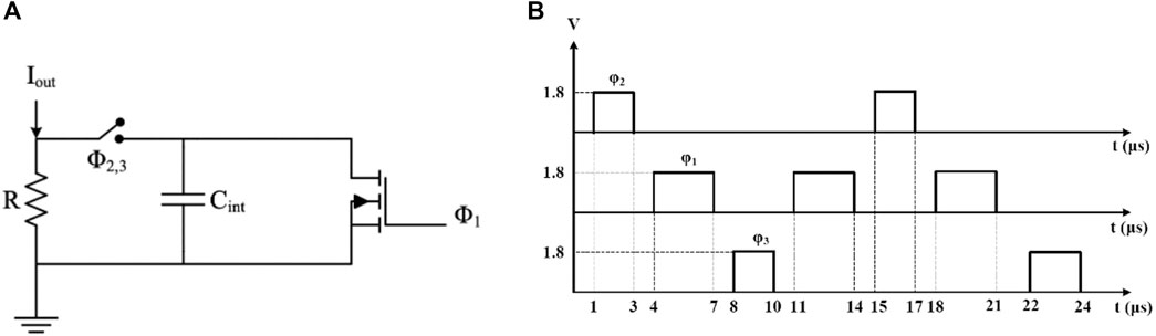
FIGURE 3. RC Integrating Circuit (A) and clock waveforms of φ1, φ2 and φ3(B).
Calibration
One of the common problems in biosensors is due to remaining analyte after one sensing procedure, or because of mismatches in analog circuits. Mismatches may cause some sensing inaccuracies even before sensing procedure starts. These two problems may cause a non-zero sensor response when no analyte is exposed to the sensor. This non-zero initial voltage usually alters the final measured voltage of the sensing structure. The integrated circuit should be able to cancel this non-zero response. There are two main readout architectures for biosensors. One possible architecture is the reference-less structure in which, there is only one electrode which is exposed to the target analyte. This architecture consumes less power, because of the minimized number of sensing branches. The other architecture is a referenced structure which employs a reference branch in addition to the original sensing branch. Although such structures consume more power because of the doubled readout circuit, they are more advantageous in terms of sensitivity and accuracy. (Couniot et al., 2016; Senevirathna et al., 2019; Taheri and Mirhassani, 2021).
The new OFET-based referenced readout circuit includes a calibration circuit which enables the sensor to cancel the output offset. The calibration circuit uses a programmable current source circuit, shown in Figure 4A, to withdraw the excessive charge on the integrating capacitance, which has resulted in the offset voltage. This calibration circuit is composed of four identical voltage comparators which are sensitive to voltage differences as low as 1 mV. The structure of voltage comparators are shown in Figure 4B, whereas Figure 4C shows the voltage comparator performance. Based on the value of the offset voltage, which is compared to four reference voltages, the four branches of the calibration circuit are activated. Each branch withdraws some charge from the integrating capacitance, until the offset voltage is cancelled. The calibration circuit is activated before sensing interval. As shown in Figure 4A, the calibration circuit is composed of four sensitive comparators which their output signals activate four current branches. If there is any offset voltage larger than 1 mV at the end of the calibration phase, the comparators will activate an independent current source which its output is applied to the sensing RC circuit. These extra currents will set the output voltage of the RC circuit to zero; the offset voltage will be cancelled, and the sensing circuit will be calibrated. The proper connection node of the calibration circuit, which is not going to have a great influence on its functionality, will be investigated in future works. Using this calibration scheme the output offset voltage of the sensor in minimized as much as possible regardless of the sources of offset voltage. We tested our calibration method for the offset of the sensor at different corner cases of the technology. The resulting performance is shown in Table 2. Importantly, the calibration scheme results in significantly reduced offset voltages even for low values of the output offset.
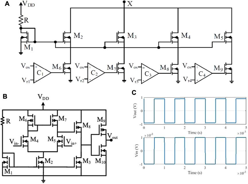
FIGURE 4. Diagrams of (A) the calibration circuit, (B) voltage comparator circuit, and (C) voltage comparator input (down) and output (up) voltage waveforms.
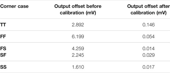
TABLE 2. Calibration circuit performance at different corner cases, described as FF (Fast NMOS, Fast PMOS), FS (Fast NMOS, Slow PMOS), SF (Slow NMOS, Fast PMOS), and SS (Slow NMOS, Slow PMOS).
Conclusion
In summary, a CMOS integrated readout circuit for OFET-based smart sensors has been designed and results from simulation have been discussed. Specifically, the analog circuit was designed to receive and amplify the drain current variations of an OFET as a result of the exposure to a targeted analyte. Importantly, the proposed architecture measures the variations of the drain current of the OFETs in three different phases so-called reset, calibration, and exposure phase. Using these three phases, the readout circuit is able to cancel out any offset due to remained analytes. With a fully differential sensing structure, and the proposed calibration circuit, the output offset, the common-mode based errors, and the hysteresis of the OFET are minimized. With a power consumption of 571 μW, the proposed structure is a promising candidate for low-power, portable sensing applications. Given the increased interest toward conformable and stretchable sensors, the new sensor design also enables to accommodate any change in channel geometry upon strain, which typically has to be accounted for in conventional OFETs to get an accurate measure of the charge mobility and drain current. The new circuit allows for a facile change in the voltage applied, allowing to make up for the drop-in current by simply varying the voltage in order to maintain the current measured in the device. The results obtained from the simulation are an important step toward the design of new smart sensors capable of detecting a wide variety of analytes, including gas and organic liquids, directly at the point of care.
Experimental Procedure
The proposed readout circuit has been designed and simulated in Cadence, using CMOS 0.18 μm process. Powered by a 1.8 V power supply, all of the circuits were designed and simulated using custom designed MOS transistors, with minimized number of control signals, to implement a fully integrated, autonomous readout structure.
Data Availability Statement
The raw data supporting the conclusion of this article will be made available by the authors, without undue reservation.
Author Contributions
MM and SR-G conceived and directed the project. HT and MM performed all simulations and data analysis. MO and PBJSO helped with the discussion. All the co-authors wrote the manuscript and commented on it during its preparation.
Funding
This work was supported by NSERC through a Discovery Grant (No. RGPIN-2017–06611). SR-G also acknowledges the University of Windsor for financial support. The authors declare no competing financial interest.
Conflict of Interest
The authors declare that the research was conducted in the absence of any commercial or financial relationships that could be construed as a potential conflict of interest.
Publisher’s Note
All claims expressed in this article are solely those of the authors and do not necessarily represent those of their affiliated organizations, or those of the publisher, the editors, and the reviewers. Any product that may be evaluated in this article, or claim that may be made by its manufacturer, is not guaranteed or endorsed by the publisher.
Acknowledgments
MO thanks NSERC for support through a post-graduate doctoral scholarship. PBJSO thanks the Government of Ontario for financial support through an Ontario Graduate Scholarship (OGS).
References
Adhikari, B., and Majumdar, S. (2004). Polymers in Sensor Applications. Prog. Polym. Sci. 29, 699–766. doi:10.1016/j.progpolymsci.2004.03.002
Asplund, M., Nyberg, T., and Inganäs, O. (2010). Electroactive Polymers for Neural Interfaces. Polym. Chem. 1, 1374–1391. doi:10.1039/c0py00077a
Bae, G. Y., Pak, S. W., Kim, D., Lee, G., Kim, D. H., Chung, Y., et al. (2016). Linearly and Highly Pressure-Sensitive Electronic Skin Based on a Bioinspired Hierarchical Structural Array. Adv. Mater. 28, 5300–5306. doi:10.1002/adma.201600408
Baude, P. F., Ender, D. A., Haase, M. A., Kelley, T. W., Muyres, D. V., and Theiss, S. D. (2003). Pentacene-Based Radio-Frequency Identification Circuitry. Appl. Phys. Lett. 82, 3964–3966. doi:10.1063/1.1579554
Bhalla, N., Di Lorenzo, M., Estrela, P., and Pula, G. (2017). Semiconductor Technology in Protein Kinase Research and Drug Discovery: Sensing a Revolution. Drug Discov. Today 22, 204–209. doi:10.1016/j.drudis.2016.10.006
Couniot, N., Francis, L. A., and Flandre, D. (2016). A 16 X 16 CMOS Capacitive Biosensor Array Towards Detection of Single Bacterial Cell. IEEE Trans. Biomed. Circuits Syst. 10, 364–374. doi:10.1109/tbcas.2015.2416372
Faraji, S., Hashimoto, T., Turner, M. L., and Majewski, L. A. (2015). Solution-Processed Nanocomposite Dielectrics for Low Voltage Operated OFETs. Org. Electron. 17, 178–183. doi:10.1016/j.orgel.2014.12.010
Feng, L., Tang, W., Zhao, J., Yang, R., Hu, W., Li, Q., et al. (2016). Unencapsulated Air-Stable Organic Field Effect Transistor by All Solution Processes for Low Power Vapor Sensing. Sci. Rep. 6, 20671–20679. doi:10.1038/srep20671
Frick, V., Leveque, P., Soysal, U., and Heiser, T. (2016). “Integrated High-Voltage CMOS Mixed-Signal Instrumentation System for OFET-Based Gas Sensor,” in 2016 IEEE International Conference on Electronics, Circuits and Systems (ICECS), Monte Carlo, Monaco, December 11–14, 2016, 309–312. doi:10.1109/icecs.2016.7841194
Gonçalves, D., Prazeres, D. M. F., Chu, V., and Conde, J. P. (2008). Detection of DNA and Proteins Using Amorphous Silicon Ion-Sensitive Thin-Film Field Effect Transistors. Biosens. Bioelectron. 24, 545–551. doi:10.1016/j.bios.2008.05.006
Gubbi, J., Buyya, R., Marusic, S., and Palaniswami, M. (2013). Internet of Things (IoT): A Vision, Architectural Elements, and Future Directions. Future Gen. Comput. Syst. 29, 1645–1660. doi:10.1016/j.future.2013.01.010
Hammock, M. L., Chortos, A., Tee, B. C.-K., Tok, J. B.-H., and Bao, Z. (2013). 25th Anniversary Article: The Evolution of Electronic Skin (E-Skin): A Brief History, Design Considerations, and Recent Progress. Adv. Mater. 25, 5997–6038. doi:10.1002/adma.201302240
Irimia-Vladu, M. (2014). "Green" Electronics: Biodegradable and Biocompatible Materials and Devices for Sustainable Future. Chem. Soc. Rev. 43, 588–610. doi:10.1039/c3cs60235d
Isaksson, J., Kjäll, P., Nilsson, D., Robinson, N., Berggren, M., and Richter-Dahlfors, A. (2007). Electronic Control of Ca2+ Signalling in Neuronal Cells Using an Organic Electronic Ion Pump. Nat. Mater 6, 673–679. doi:10.1038/nmat1963
Kato, Y., Sekitani, T., Takamiya, M., Doi, M., Asaka, K., Sakurai, T., et al. (2007). Sheet-Type Braille Displays by Integrating Organic Field-Effect Transistors and Polymeric Actuators. IEEE Trans. Electron. Devices 54, 202–209. doi:10.1109/ted.2006.888678
Knopfmacher, O., Hammock, M. L., Appleton, A. L., Schwartz, G., Mei, J., Lei, T., et al. (2014). Highly Stable Organic Polymer Field-Effect Transistor Sensor for Selective Detection in the Marine Environment. Nat. Commun. 5, 2954. doi:10.1038/ncomms3954
Lai, S., Demelas, M., Casula, G., Cosseddu, P., Barbaro, M., and Bonfiglio, A. (2013). Ultralow Voltage, OTFT-Based Sensor for Label-free DNA Detection. Adv. Mater. 25, 103–107. doi:10.1002/adma.201202996
Lee, M. Y., Kim, H. J., Jung, G. Y., Han, A.-R., Kwak, S. K., Kim, B. J., et al. (2015). Highly Sensitive and Selective Liquid-phase Sensors Based on a Solvent-Resistant Organic-Transistor Platform. Adv. Mater. 27, 1540–1546. doi:10.1002/adma.201404707
Lei, K.-M., Mak, P.-I., Law, M.-K., and Martins, R. P. (2016). CMOS Biosensors for In Vitro Diagnosis - Transducing Mechanisms and Applications. Lab. Chip 16, 3664–3681. doi:10.1039/c6lc01002d
Li, Q., Zhao, J., Huang, Y., Tang, W., Peng, S., Qiu, S., et al. (2018). Integrated Low Voltage Ion Sensing Organic Field Effect Transistor System on Plastic. IEEE Electron. Device Lett. 39, 591–594. doi:10.1109/led.2018.2808192
Liao, C., Zhang, M., Yao, M. Y., Hua, T., Li, L., and Yan, F. (2015). Flexible Organic Electronics in Biology: Materials and Devices. Adv. Mater. 27, 7493–7527. doi:10.1002/adma.201402625
Mei, J., and Bao, Z. (2014). Side Chain Engineering in Solution-Processable Conjugated Polymers. Chem. Mater. 26 (1), 604–615. doi:10.1021/cm4020805
Murmann, B., and Xiong, W. (2010). “Design of Analog Circuits Using Organic Field-Effect Transistors,” in IEEE/ACM International Conference on Computer-Aided Design (ICCAD), San Jose, CA, November 7–11, 2010, 504–507. doi:10.1109/iccad.2010.5653805
O'Connor, T. F., Rajan, K. M., Printz, A. D., and Lipomi, D. J. (2015). Toward Organic Electronics with Properties Inspired by Biological Tissue. J. Mater. Chem. B 3, 4947–4952. doi:10.1039/c5tb00173k
Ocheje, M. U., Charron, B. P., Nyayachavadi, A., and Rondeau-Gagné, S. (2017). Stretchable Electronics: Recent Progress in the Preparation of Stretchable and Self-Healing Semiconducting Conjugated Polymers. Flex. Print. Electron. 2, 043002. doi:10.1088/2058-8585/aa9c9b
Ocheje, M. U., Selivanova, M., Zhang, S., Van Nguyen, T. H., Charron, B. P., Chuang, C.-H., et al. (2018). Influence of Amide-Containing Side Chains on the Mechanical Properties of Diketopyrrolopyrrole-Based Polymers. Polym. Chem. 9, 5531–5542. doi:10.1039/c8py01207e
Ogunleye, O. O., Sakai, H., Ishii, Y., and Murata, H. (2019). Investigation of the Sensing Mechanism of Dual-Gate Low-Voltage Organic Transistor Based Pressure Sensor. Org. Electron. 75, 105431. doi:10.1016/j.orgel.2019.105431
Oh, J. Y., Rondeau-Gagné, S., Chiu, Y.-C., Chortos, A., Lissel, F., Wang, G.-J. N., et al. (2016). Intrinsically Stretchable and Healable Semiconducting Polymer for Organic Transistors. Nature 539, 411–415. doi:10.1038/nature20102
Rivnay, J., Owens, R. M., and Malliaras, G. G. (2014). The Rise of Organic Bioelectronics. Chem. Mater. 26, 679–685. doi:10.1021/cm4022003
Roberts, M. E., Mannsfeld, S. C. B., Queraltó, N., Reese, C., Locklin, J., Knoll, W., et al. (2008). Water-Stable Organic Transistors and Their Application in Chemical and Biological Sensors. Proc. Natl. Acad. Sci. 105, 12134–12139. doi:10.1073/pnas.0802105105
Rogers, J. A., and Bao, Z. (2002). Printed Plastic Electronics and Paperlike Displays. J. Polym. Sci. A. Polym. Chem. 40, 3327–3334. doi:10.1002/pola.10405
Schwartz, G., Tee, B. C.-K., Mei, J., Appleton, A. L., Kim, D. H., Wang, H., et al. (2013). Flexible Polymer Transistors with High Pressure Sensitivity for Application in Electronic Skin and Health Monitoring. Nat. Commun. 4, 1859. doi:10.1038/ncomms2832
Senevirathna, B., Lu, S., Dandin, M., Basile, J., Smela, E., and Abshire, P. (2019). High Resolution Monitoring of Chemotherapeutic Agent Potency in Cancer Cells Using a CMOS Capacitance Biosensor. Biosens. Bioelectron. 142, 111501. doi:10.1016/j.bios.2019.111501
Senthamizhan, A., Fragouli, D., Balusamy, B., Patil, B., Palei, M., Sabella, S., et al. (2019). Hydrochromic Carbon Dots as Smart Sensors for Water Sensing in Organic Solvents. Nanoscale Adv. 1, 4258–4267. doi:10.1039/c9na00493a
Sirringhaus, H. (2014). 25th Anniversary Article: Organic Field-Effect Transistors: The Path Beyond Amorphous Silicon. Adv. Mater. 26, 1319–1335. doi:10.1002/adma.201304346
Someya, T., Sekitani, T., Iba, S., Kato, Y., Kawaguchi, H., and Sakurai, T. (2004). A Large-Area, Flexible Pressure Sensor Matrix with Organic Field-Effect Transistors for Artificial Skin Applications. Proc. Natl. Acad. Sci. 101, 9966–9970. doi:10.1073/pnas.0401918101
Su, B., Gong, S., Ma, Z., Yap, L. W., and Cheng, W. (2015). Mimosa-Inspired Design of a Flexible Pressure Sensor with Touch Sensitivity. Small 11, 1886–1891. doi:10.1002/smll.201403036
Taheri, H. E., and Mirhassani, M. (2021). A Low-Power, High-Resolution, Adaptive Sensitivity Readout Circuit with Selective Detection Range for Capacitive Biosensors. AEU Int. J. Electron. Commun. 131, 153599. doi:10.1016/j.aeue.2020.153599
Tang, W., Jiang, C., Li, Q., Hu, W., Feng, L., Huang, Y., et al. (2016). Low-Voltage PH Sensor Tag Based on All Solution Processed Organic Field-Effect Transistor. IEEE Electron. Device Lett. 37, 1002–1005. doi:10.1109/led.2016.2580565
Torsi, L., Magliulo, M., Manoli, K., and Palazzo, G. (2013). Organic Field-Effect Transistor Sensors: A Tutorial Review. Chem. Soc. Rev. 42, 8612. doi:10.1039/c3cs60127g
Uslu, F., Ingebrandt, S., Mayer, D., Böcker-Meffert, S., Odenthal, M., and Offenhäusser, A. (2004). Labelfree Fully Electronic Nucleic Acid Detection System Based on a Field-Effect Transistor Device. Biosens. Bioelectron. 19, 1723–1731. doi:10.1016/j.bios.2004.01.019
Velliste, M., Perel, S., Spalding, M. C., Whitford, A. S., and Schwartz, A. B. (2008). Cortical Control of a Prosthetic Arm for Self-Feeding. Nature 453, 1098–1101. doi:10.1038/nature06996
Wen, H.-F., Wu, H.-C., Aimi, J., Hung, C.-C., Chiang, Y.-C., Kuo, C.-C., et al. (2017). Soft Poly(Butyl Acrylate) Side Chains toward Intrinsically Stretchable Polymeric Semiconductors for Field-Effect Transistor Applications. Macromolecules 50, 4982–4992. doi:10.1021/acs.macromol.7b00860
Wu, H.-C., Hung, C.-C., Hong, C.-W., Sun, H.-S., Wang, J.-T., Yamashita, G., et al. (2016). Isoindigo-Based Semiconducting Polymers Using Carbosilane Side Chains for High Performance Stretchable Field-Effect Transistors. Macromolecules 49, 8540–8548. doi:10.1021/acs.macromol.6b02145
Xu, J., Wang, S., Wang, G. N., Zhu, C., Luo, S., Jin, L., et al. (2017). Highly Stretchable Polymer Semiconductor Films through the Nanoconfinement Effect. Science 355, 59–64. doi:10.1126/science.aah4496
Zhan, Y., Mei, Y., and Zheng, L. (2014). Materials Capability and Device Performance in Flexible Electronics for the Internet of Things. J. Mater. Chem. C 2, 1220–1232. doi:10.1039/c3tc31765j
Keywords: CMOS readout integrated circuit, organic field-effect transistors, biosensor, smart sensors, stretchable materials, semiconducting polymers
Citation: Taheri HE, Ocheje MU, St. Onge PBJ, Rondeau-Gagné S and Mirhassani M (2021) Computational Design of an Integrated CMOS Readout Circuit for Sensing With Organic Field-Effect Transistors. Front. Electron. 2:725008. doi: 10.3389/felec.2021.725008
Received: 14 June 2021; Accepted: 19 August 2021;
Published: 03 September 2021.
Edited by:
Manan Suri, Indian Institute of Technology Delhi, IndiaReviewed by:
Xinge Yu, City University of Hong Kong, Hong Kong, SAR ChinaBibhu Datta Sahoo, Indian Institute of Technology Kharagpur, India
Copyright © 2021 Taheri, Ocheje, St. Onge, Rondeau-Gagné and Mirhassani. This is an open-access article distributed under the terms of the Creative Commons Attribution License (CC BY). The use, distribution or reproduction in other forums is permitted, provided the original author(s) and the copyright owner(s) are credited and that the original publication in this journal is cited, in accordance with accepted academic practice. No use, distribution or reproduction is permitted which does not comply with these terms.
*Correspondence: Mitra Mirhassani, bWl0cmFtaXJAdXdpbmRzb3IuY2E=; Simon Rondeau-Gagné, c3JvbmRlYXVAdXdpbmRzb3IuY2E=