 Alfred Zhao1
 Jason A. Röhr
94% of researchers rate our articles as excellent or good
Learn more about the work of our research integrity team to safeguard the quality of each article we publish.
Find out more
PERSPECTIVE article
Front. Electron. Mater, 17 May 2024
Sec. Semiconducting Materials and Devices
Volume 4 - 2024 | https://doi.org/10.3389/femat.2024.1396521
This article is part of the Research TopicCelebrating 3 Years of Frontiers in Electronic MaterialsView all 4 articles
Space-charge-limited current (SCLC) measurements are commonly employed to characterize charge-transport properties of semiconductors used in next-generation thin-film optoelectronics, such as organic
Space-charge-limited current (SCLC) measurements (Mott and Gurney, 1940; Dacey, 1953; Shockley and Prim, 1953; Rose, 1955), a class of steady-state DC charge-transport measurements, have become near-ubiquitous within the organic and metal-halide perovskite optoelectronics communities as a tool for estimating key characteristics influencing the performance of solar cells and light-emitting diodes: charge-carrier mobilities, defect characteristics, injection properties, and energetic disorder (Poplavskyy and Nelson, 2003; Van Mensfoort and Coehoorn, 2008; Dacuña and Salleo, 2011; Coehoorn and Bobbert, 2012; Röhr et al., 2018b; Kotadiya et al., 2018; 2019; Lee et al., 2018; Shi et al., 2019; Duijnstee et al., 2020; Sajedi Alvar et al., 2020; Duijnstee et al., 2021; Le Corre et al., 2021; Sachnik et al., 2023; Trieb et al., 2023). Some of the appeals of SCLC measurements include the apparent simplicity of the method and the ability to selectively probe either electron or hole transport through careful design of the single-carrier devices used to perform these measurements. However, while these devices are relatively simple to design and fabricate, the interdependence and magnitudes of the probed characteristics not only complicate the analysis of the obtained current density-voltage (J-V) curves (Röhr et al., 2018b), but also determine the limits of what SCLC measurements can realistically probe (Röhr and MacKenzie, 2020; Le Corre et al., 2021; Röhr, 2024).
Single-carrier devices can be designed to exclusively conduct either electrons or holes by carefully matching the electrode work functions with either the conduction- or valence band-edges of the semiconductor, in which case they are often referred to as either electron- or hole-only devices, respectively (Figure 1A). The work function of a conductor,
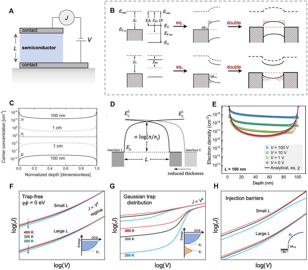
Figure 1. (A), Schematic of a typical sandwich-type single-carrier device, with the probed semiconductor placed between two similar contacts with spacing L. The contact spacing is equal to the semiconductor thickness in this type of device. (B), Energy level diagrams of conductor-semiconductor interfaces, the formation of near-ohmic contacts at equilibrium, and the formation of single-carrier devices. (C), Comparison between background charge-carrier density and intrinsic charge-carrier density in a single-carrier device with either L = 100 nm or L = 1 cm (Röhr et al., 2017). (D), Schematic showing why reducing thickness leads to an increase in charge-carrier density (Röhr et al., 2017). (E), Electron density of an electron-only device under various applied voltages shown in comparison with Eq. 2 (Röhr and MacKenzie, 2020). (F), Conceptual J-V curves from an SCLC measurement where an intrinsic semiconductor is measured, showing the effect from varying device temperature (from 200 K to 400 K) and thickness. The Mott-Gurney law can be employed in the
Once a single-carrier device is made, SCLC measurements are performed by applying a voltage, V, across the device and measuring the current density, J (Figure 1A). Analyzing the resulting J-V curves can appear to be a relatively simple procedure. In fact, many studies rely on a fitting procedure with a simplistic analytical model, the Mott-Gurney law (Mott and Gurney, 1940), to extract charge-carrier mobilities,
where
Analytical and numerical models exist that attempt to account for the non-ideal behavior described above (Lampert, 1956; Mark and Helfrich, 1962; Murgatroyd, 1970; Dacuña and Salleo, 2011; De Bruyn et al., 2013; Röhr et al., 2018b; Röhr and MacKenzie, 2020; Koopmans et al., 2022). However, to extract meaningful charge-transport characteristics from SCLC data, a “correct” model must be identified for fitting. Identifying a correct model can be difficult, especially when novel materials are being explored and the underlying physics governing charge-transport behavior is not yet understood. Therefore, the default is often to use the simplest model possible that appears to describe a given data set reasonably well. Nonetheless, wrongful characteristics can easily be obtained if the applied model is imprecise in describing the particular material being probed. Fortunately, SCLC data is temperature and device thickness dependent, and will typically show variations corresponding to specific non-idealities influencing charge transport in the material (Dacuña and Salleo, 2011; Röhr et al., 2018b). Examples of this are conceptually shown in Figures 1F–H. Varying the device temperature between each measurement, and measuring a set of devices with different semiconductor thickness, will result in distinct fingerprints in the J-V data that can greatly help in identifying what underlying physics is governing charge transport (Zuo et al., 2017; Röhr et al., 2018b; Shi et al., 2019; Zuo et al., 2019). Although this gives rise to some added complexity during data analysis, the result is a more accurate and trustworthy interpretation.
While the device temperature and thickness dependence on SCLC J-V curves, and how these dependencies can be used during characterization, have been discussed to some length in the literature (Poplavskyy and Nelson, 2003; Dacuña and Salleo, 2011; Röhr et al., 2018b; Kotadiya et al., 2018), less attention has been put towards understanding what the ultimate limits for SCLC measurements truly are. We now understand that there exist temperature and device thickness dependent limits on the minimal doping and trap densities that allow for detection by SCLC measurements (Röhr and MacKenzie, 2020; Le Corre et al., 2021). So while it may appear that a probed semiconductor is not influenced by defects or impurities, it could simply be that the density is below the detection threshold for that particular device at the probed temperature. The same is true for injection barriers (Röhr, 2024). Luckily, simple conditions can now be stated for when these non-idealities are masked (Röhr and MacKenzie, 2020; Le Corre et al., 2021; Röhr, 2024). So while these limits could potentially be considered as a downside of SCLC, they could potentially be used as an additional tool.
Herein, we discuss why J-V curves obtained from SCLC measurements are often highly device thickness and temperature dependent. We subsequently discuss why the choice of device thickness and temperature determines at what threshold which characteristics can be extracted from SCLC measurements. Finally, we present examples where thickness and temperature variation was used to increase the accuracy of fitting procedures, and therefore the accuracy of the data analysis and extracted material and device characteristics.
The thickness and temperature dependance of SCLC J-V curves can be understood from examining mathematical descriptions of the free, equilibrium/background charge-carrier density inside an intrinsic semiconductor sandwiched by ohmic contacts under zero applied bias (Figures 1C, E). This is the case whether the semiconductor contains defects (either acting as trap sites or as dopants) and/or injection barriers, or not, as defects and injection barriers alter the background charge-carrier density that is responsible for the current flow while also adding their individual temperature dependencies, increasing the overall complexity. We can therefore learn a lot simply from considering how the unaltered, background charge-carrier density varies with thickness and temperature.
In the absence of defects and injection barriers, the total charge-carrier density,
Out of these quantities,
where,
From Eq. (3), it is evident that both the equilibrium charge-carrier density and the injected density are highly influenced by varying the thickness due to the L-2 terms and that the equilibrium charge-carrier density is additionally affected by temperature via the thermal energy term. Inserting
which describes SCLC from the low-voltage regime (first term in Eq. 4) up through the Mott-Gurney regime (second term in Eq. 4). This means that even in a highly idealized case where the semiconductor is not influenced by defects and injection barriers, the J-V response is still influenced by T and L.
Defects giving rise to trap states can have a profound impact on the current flow in the device as a fraction of the total free charge-carrier density can get immobilized in these states (Hall, 1952; Shockley and Read, 1952; Lampert, 1956; Mark and Helfrich, 1962). A large density of trap states,
Besides using thickness variations for characterization, L also determines when traps are entirely screened in the J-V curves. If the background charge-carrier density exceeds the trap density, then the detrimental effects from said traps are diminished. So, while trap states might indeed be present in the semiconductor, even in large quantities, they will sometimes not be observed in the J-V curves, and incorrect conclusions about their presence might be drawn. In fact, it has been shown that a condition for when traps influence a single-carrier device can be derived by noting that
As this quantity is linearly proportional to device temperature and inversely square proportional to the device thickness, we now have qualitative means to understand how varying these quantities will affect whether traps can be observed from the measurement. As an example, we will consider a single-carrier device with L = 200 nm,
This has two rather significant consequences. On the one hand, devices (or experiments) can be designed where the traps are masked, which would allow for a cleaner extraction of the charge-carrier mobility (with Eq. 4 for example,) as traps would not have to be explicitly accounted for during the data analysis. On the other hand, one can accidentally draw the wrongful conclusion that the semiconductor being probed is “trap-free” which could have detrimental impacts on future research into the probed materials and associated devices. However, conducting a series of experiments varying L and T should aid in reducing these wrongful conclusions.
Analogous to the conditions describing when traps are screened in SCLC J-V curves, dopants can similarly be screened if the background charge-carrier density is larger than the density of ionized dopants. Additionally, conditions can be written for the cases where injection barriers, resulting from non-zero injection barriers at the semiconductor/contact interfaces, are no longer influencing the current response.
Dopants are defects that are chosen and incorporated into a semiconductor in a way that ensures that most are thermally ionized at room temperature, i.e., their ionization energies are so low that they are almost guaranteed to grant a charge carrier (e.g., boron dopants in silicon). It is thereby possible to tune the electronic properties of the semiconductor depending on the type of charge carrier introduced. A consequence of dopant ionization energies being so low is that increasing the temperature will not yield any significant additional charge carriers and decreasing the temperature will not result in a significant decrease in the charge-carrier density either (unless the semiconductor is cooled down to very low temperatures). The density of ionized dopants,
Regardless of the density of ionized dopants being relatively constant with temperature, the device thickness and temperature will still determine when dopants are screened in SCLC J-V curves. Similar to the case of traps, if the background charge-carrier density is exceedingly high, then the effects from said dopants are diminished. A similar condition can therefore be written (Röhr and MacKenzie, 2020),
and the example that was made for the case where the semiconductor contained traps can likewise be made for case where the semiconductor is doped.
In the case of non-ohmic contacts, the temperature dependence can be understood from the effect of having injection barriers at the interfaces,
where
Similar to the previous cases, for a device with L = 200 nm,
While the common approach for estimating mobilities using SCLC is to simply fit with the Mott-Gurney law to data from a single device, we and others have used more comprehensive approaches of varying device temperature and measuring devices with different thicknesses to not only improve the accuracy of the analysis but to also obtain characteristics beyond simply the charge-carrier mobility (Wetzelaer et al., 2012; Röhr et al., 2018b). This has been done with both analytical models (including the Mott-Gurney law) and more sophisticated drift-diffusion models. To highlight this, and to hopefully inspire researchers to adopt such approaches, below we focus on a few examples from within the organic electronics communities where important and surprising results were obtained.
In 2018, Kotadiya et al., 2018 employed SCLC measurements, observing transitions from injection-limited to space-charge-limited current, to show that injection from transition-metal oxide hole contacts into a range of organic semiconductors with high ionization potentials can be made ohmic by introducing a thin interlayer of TCTA. To verify this, they measured a large set of hole-only devices where the only variable was the device thickness, and showed that a constant mobility could be extracted for each material, independent of the device thickness (Figure 2A). The following year, Kotadiya et al., 2019 again used SCLC to explore trap states in a large library of semiconducting polymers, small molecules, and fullerene derivatives, using varying device thickness as part of their extensive analysis. They found that hole and electron transport is trap-limited for the investigated materials if they have ionization potentials higher than 6.0 eV and electron affinities smaller than 3.6 eV, respectively (Figures 2B,C). They concluded that these trapping events are caused by water clusters inside the semiconducting films.
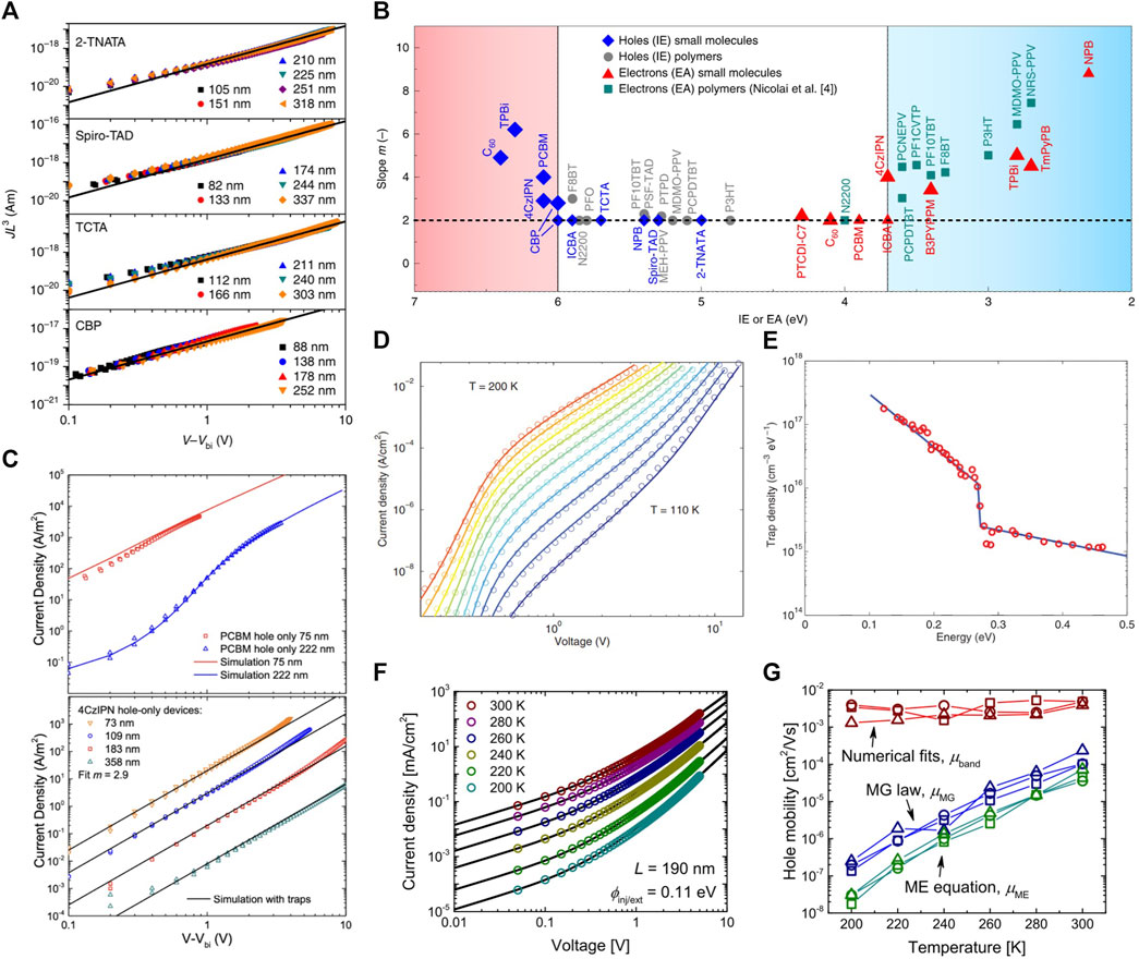
Figure 2. (A), SCLC J-V curves, obtained from four different organic materials with varying device thickness. The y-axis has been corrected to easily show that the curves are thickness independent and that the J-V curves approximate a square-law dependence:
In 2011, Dacuña and Salleo used a drift-diffusion approach to model SCLC data obtained from an organic rubrene single-crystal measured at temperatures varying from 110 K to 200 K (Figure 2D) (Krellner et al., 2007; Dacuña and Salleo, 2011). By fitting their model across the entire range of SCLC data, they were able to conclude that the sub-band density of states is well-modeled by a piecewise exponential function of trap states (Figure 2E). They also showed that while gold contacts were used on either side of the crystal, as one contact was deposited via evaporation while the other was electrostatically laminated, this resulted in two different metal/semiconductor interfaces, thereby resulting in significant contact asymmetry and therefore a built-in voltage that was essential to account for in the low-voltage regime during fitting procedures.
Finally, SCLC measurements have also been employed to investigate hole transport in pristine spiro-OMeTAD (Röhr et al., 2018b), an organic hole-transport material that has historically been used in solid-state dye-sensitized solar cells (Cappel et al., 2012) and which is now commonly used in perovskite solar cells (Kong et al., 2021). We measured a set of hole-only devices with increasing spiro-OMeTAD thickness (115 nm, 190 nm, and 290 nm) across temperatures ranging from 200 K to 300 K (the data from L = 190 nm case are shown in Figure 2F). The data was analyzed with both simple analytical models (Eq. 1 and first term in Eq. 4) and a drift-diffusion model that could explicitly account for trapping, injection barriers, and external resistances. It was shown that while the use of analytical models yielded a highly temperature-dependent “effective” mobility, the band-like mobility obtained from fitting with the drift-diffusion model did not yield as drastic of a temperature dependence while also yielding an overall higher mobility (Figure 2G). This highlights the importance of explicitly accounting for traps and injection barriers when analyzing SCLC data, and how varying both temperature and thickness will aid in this analysis.
We here highlighted the importance of not only measuring devices with different thicknesses, but also measuring such devices at varying temperature in order to achieve accurate device and materials characteristics from SCLC measurements. We also highlighted how the choice of device thickness and temperature is critical in determining what characteristics can realistically be extracted from SCLC measurements, and how erroneous conclusions can potentially be drawn about the probed semiconducting material if this is not considered. While this perspective is not extensive in scope, as other factors could affect the outcome of an SCLC measurement and the subsequent analysis, we hope that the topics covered herein will initiate a broader discussion into SCLC metrology while also aiding in improving charge-transport characterization of thin-film semiconductors.
The original contributions presented in the study are included in the article/Supplementary material, further inquiries can be directed to the corresponding author/s.
AZ: Conceptualization, Writing–review and editing. VL: Conceptualization, Investigation, Writing–review and editing. JR: Conceptualization, Investigation, Supervision, Writing–original draft, Writing–review and editing.
The author(s) declare that no financial support was received for the research, authorship, and/or publication of this article.
The authors declare that the research was conducted in the absence of any commercial or financial relationships that could be construed as a potential conflict of interest.
All claims expressed in this article are solely those of the authors and do not necessarily represent those of their affiliated organizations, or those of the publisher, the editors and the reviewers. Any product that may be evaluated in this article, or claim that may be made by its manufacturer, is not guaranteed or endorsed by the publisher.
Cappel, U. B., Daeneke, T., and Bach, U. (2012). Oxygen-Induced doping of spiro-MeOTAD in solid-state dye-sensitized solar cells and its impact on device performance. Nano Lett. 12, 4925–4931. doi:10.1021/nl302509q
Coehoorn, R., and Bobbert, P. A. (2012). Effects of Gaussian disorder on charge carrier transport and recombination in organic semiconductors. Phys. Status Solidi (a) 209, 2354–2377. doi:10.1002/pssa.201228387
Dacey, G. C. (1953). Space-charge limited hole current in germanium. Phys. Rev. 90, 759–763. doi:10.1103/PhysRev.90.759
Dacuña, J., and Salleo, A. (2011). Modeling space-charge-limited currents in organic semiconductors: extracting trap density and mobility. Phys. Rev. B 84, 195209. doi:10.1103/PhysRevB.84.195209
De Bruyn, P., Van Rest, A. H. P., Wetzelaer, G. A. H., De Leeuw, D. M., and Blom, P. W. M. (2013). Diffusion-limited current in organic metal-insulator-metal diodes. Phys. Rev. Lett. 111, 186801. doi:10.1103/PhysRevLett.111.186801
Duijnstee, E. A., Ball, J. M., Le Corre, V. M., Koster, L. J. A., Snaith, H. J., and Lim, J. (2020). Toward understanding space-charge limited current measurements on metal halide perovskites. ACS Energy Lett. 5, 376–384. doi:10.1021/acsenergylett.9b02720
Duijnstee, E. A., Le Corre, V. M., Johnston, M. B., Koster, L. J. A., Lim, J., and Snaith, H. J. (2021). Understanding dark current-voltage characteristics in metal-halide perovskite single crystals. Phys. Rev. Appl. 15, 014006. doi:10.1103/PhysRevApplied.15.014006
Hall, R. N. (1952). Electron-hole recombination in germanium. Phys. Rev. 87, 387. doi:10.1103/PhysRev.87.387
Kong, J., Shin, Y., Röhr, J. A., Wang, H., Meng, J., Wu, Y., et al. (2021). CO2 doping of organic interlayers for perovskite solar cells. Nature 594, 51–56. doi:10.1038/s41586-021-03518-y
Koopmans, M., Corre, V., and Koster, L. (2022). SIMsalabim: an open-source drift-diffusion simulator for semiconductor devices. JOSS 7, 3727. doi:10.21105/joss.03727
Kotadiya, N. B., Lu, H., Mondal, A., Ie, Y., Andrienko, D., Blom, P. W. M., et al. (2018). Universal strategy for Ohmic hole injection into organic semiconductors with high ionization energies. Nat. Mater 17, 329–334. doi:10.1038/s41563-018-0022-8
Kotadiya, N. B., Mondal, A., Blom, P. W. M., Andrienko, D., and Wetzelaer, G.-J. A. H. (2019). A window to trap-free charge transport in organic semiconducting thin films. Nat. Mat. 18, 1182–1186. doi:10.1038/s41563-019-0473-6
Krellner, C., Haas, S., Goldmann, C., Pernstich, K. P., Gundlach, D. J., and Batlogg, B. (2007). Density of bulk trap states in organic semiconductor crystals: discrete levels induced by oxygen in rubrene. Phys. Rev. B 75, 245115. doi:10.1103/PhysRevB.75.245115
Lampert, M. A. (1956). Simplified theory of space-charge-limited currents in an insulator with traps. Phys. Rev. 103, 1648–1656. doi:10.1103/PhysRev.103.1648
Le Corre, V. M., Duijnstee, E. A., El Tambouli, O., Ball, J. M., Snaith, H. J., Lim, J., et al. (2021). Revealing charge carrier mobility and defect densities in metal halide perovskites via space-charge-limited current measurements. ACS Energy Lett. 6, 1087–1094. doi:10.1021/acsenergylett.0c02599
Lee, H. K. H., Telford, A. M., Röhr, J. A., Wyatt, M. F., Rice, B., Wu, J., et al. (2018). The role of fullerenes in the environmental stability of polymer:fullerene solar cells. Energy Environ. Sci. 11, 417–428. doi:10.1039/C7EE02983G
Mark, P., and Helfrich, W. (1962). Space-charge-limited currents in organic crystals. J. Appl. Phys. 33, 205–215. doi:10.1063/1.1728487
Murgatroyd, P. N. (1970). Theory of space-charge-limited current enhanced by Frenkel effect. J. Phys. D. Appl. Phys. 3, 151–156. doi:10.1088/0022-3727/3/2/308
Poplavskyy, D., and Nelson, J. (2003). Nondispersive hole transport in amorphous films of methoxy-spirofluorene-arylamine organic compound. J. Appl. Phys. 93, 341–346. doi:10.1063/1.1525866
Röhr, J. A. (2024). On injection in intrinsic single-carrier devices. J. Comput. Electron. doi:10.1007/s10825-024-02129-w
Röhr, J. A., Kirchartz, T., and Nelson, J. (2017). On the correct interpretation of the low voltage regime in intrinsic single-carrier devices. J. Phys. Condens. Matter 29, 205901. doi:10.1088/1361-648X/aa66cc
Röhr, J. A., and MacKenzie, R. C. I. (2020). Analytical description of mixed ohmic and space-charge-limited conduction in single-carrier devices. J. Appl. Phys. 128, 165701. doi:10.1063/5.0024737
Röhr, J. A., Moia, D., Haque, S. A., Kirchartz, T., and Nelson, J. (2018a). Exploring the validity and limitations of the Mott–Gurney law for charge-carrier mobility determination of semiconducting thin-films. J. Phys. Condens. Matter 30, 105901. doi:10.1088/1361-648X/aaabad
Röhr, J. A., Shi, X., Haque, S. A., Kirchartz, T., and Nelson, J. (2018b). Charge transport in spiro-OMeTAD investigated through space-charge-limited current measurements. Phys. Rev. Appl. 9, 044017. doi:10.1103/PhysRevApplied.9.044017
Rose, A. (1955). Space-charge-limited currents in solids. Phys. Rev. 97, 1538–1544. doi:10.1103/PhysRev.97.1538
Sachnik, O., Tan, X., Dou, D., Haese, C., Kinaret, N., Lin, K.-H., et al. (2023). Elimination of charge-carrier trapping by molecular design. Nat. Mat. 22, 1114–1120. doi:10.1038/s41563-023-01592-3
Sajedi Alvar, M., Blom, P. W. M., and Wetzelaer, G.-J. A. H. (2020). Space-charge-limited electron and hole currents in hybrid organic-inorganic perovskites. Nat. Commun. 11, 4023. doi:10.1038/s41467-020-17868-0
Shi, X., Nádaždy, V., Perevedentsev, A., Frost, J. M., Wang, X., Von Hauff, E., et al. (2019). Relating chain conformation to the density of states and charge transport in conjugated polymers: the role of the β -phase in poly(9,9-dioctylfluorene). Phys. Rev. X 9, 021038. doi:10.1103/PhysRevX.9.021038
Shockley, W., and Prim, R. C. (1953). Space-charge limited emission in semiconductors. Phys. Rev. 90, 753–758. doi:10.1103/PhysRev.90.753
Shockley, W., and Read, W. T. (1952). Statistics of the recombinations of holes and electrons. Phys. Rev. 87, 835–842. doi:10.1103/PhysRev.87.835
Siekmann, J., Ravishankar, S., and Kirchartz, T. (2021). Apparent defect densities in halide perovskite thin films and single crystals. ACS Energy Lett. 6, 3244–3251. doi:10.1021/acsenergylett.1c01449
Trieb, D., Blom, P. W. M., and Wetzelaer, G. A. H. (2023). Ohmic electron injection into organic semiconductors by solution-processed and evaporated organic interlayers. Adv. Mater. Inter 10, 2202424. doi:10.1002/admi.202202424
Van Mensfoort, S. L. M., and Coehoorn, R. (2008). Effect of Gaussian disorder on the voltage dependence of the current density in sandwich-type devices based on organic semiconductors. Phys. Rev. B 78, 085207. doi:10.1103/PhysRevB.78.085207
Wetzelaer, G.-J. A. H., Kuik, M., Olivier, Y., Lemaur, V., Cornil, J., Fabiano, S., et al. (2012). Asymmetric electron and hole transport in a high-mobility n -type conjugated polymer. Phys. Rev. B 86, 165203. doi:10.1103/PhysRevB.86.165203
Zuo, G., Li, Z., Andersson, O., Abdalla, H., Wang, E., and Kemerink, M. (2017). Molecular doping and trap filling in organic semiconductor host–guest systems. J. Phys. Chem. C 121, 7767–7775. doi:10.1021/acs.jpcc.7b01758
Keywords: metrology, SCLC, charge transport, electrical characterization, defects, traps, doping, injection barriers
Citation: Zhao A, Le Corre VM and Röhr JA (2024) On the importance of varying device thickness and temperature on the outcome of space-charge-limited current measurements. Front. Electron. Mater. 4:1396521. doi: 10.3389/femat.2024.1396521
Received: 05 March 2024; Accepted: 02 April 2024;
Published: 17 May 2024.
Edited by:
Ctirad Uher, University of Michigan, United StatesReviewed by:
Kedhareswara Sairam Pasupuleti, Chungnam National University, Republic of KoreaCopyright © 2024 Zhao, Le Corre and Röhr. This is an open-access article distributed under the terms of the Creative Commons Attribution License (CC BY). The use, distribution or reproduction in other forums is permitted, provided the original author(s) and the copyright owner(s) are credited and that the original publication in this journal is cited, in accordance with accepted academic practice. No use, distribution or reproduction is permitted which does not comply with these terms.
*Correspondence: Jason A. Röhr, amFzb25yb2hyQG55dS5lZHU=
Disclaimer: All claims expressed in this article are solely those of the authors and do not necessarily represent those of their affiliated organizations, or those of the publisher, the editors and the reviewers. Any product that may be evaluated in this article or claim that may be made by its manufacturer is not guaranteed or endorsed by the publisher.
Research integrity at Frontiers
Learn more about the work of our research integrity team to safeguard the quality of each article we publish.