 Eric M. Lechner1,2
 Junki Makita
 Gianluigi Ciovati
95% of researchers rate our articles as excellent or good
Learn more about the work of our research integrity team to safeguard the quality of each article we publish.
Find out more
ORIGINAL RESEARCH article
Front. Electron. Mater , 15 August 2023
Sec. Superconducting Materials
Volume 3 - 2023 | https://doi.org/10.3389/femat.2023.1235918
This article is part of the Research Topic Progress on Superconducting Materials for SRF Applications View all 8 articles
We report radio-frequency measurements of quality factors and temperature mapping of a nitrogen doped Nb superconducting RF cavity. Cavity cutouts of hot and cold spots were studied with low temperature scanning tunneling microscopy and spectroscopy, X-ray photoelectron spectroscopy and secondary electron microscopy. Temperature mapping revealed a substantial reduction of the residual resistance upon cooling the cavity with a greater temperature gradient and hysteretic losses at the quench location, pointing to trapped vortices as the dominant source of residual surface resistance. Analysis of the tunneling spectra in the framework of a proximity effect theory shows that hot spots have a reduced pair potential and a wider distribution of the contact resistance between the Nb and the top Nb oxide. Alone, these degraded superconducting properties account for a much weaker excess dissipation as compared with the vortex contribution. Based on the correlation between the quasiparticle density of states and temperature mapping, we suggest that degraded superconducting properties may facilitate vortex nucleation or settling of trapped flux during cooling the cavity through the critical temperature.
Advances in Nb superconducting radio-frequency (SRF) cavity technology have pushed the quality factors Q0 well above 1010 and the RF breakdown fields close to the DC superheating field Hs at GHz frequencies and temperatures T < 2 K (Padamsee et al., 2008; Antoine, 2012; Gurevich, 2012; Singer et al., 2013; Padamsee, 2014; Reschke et al., 2017; Dhakal et al., 2018). Various surface and material treatments have been developed to improve the SRF performance of Nb cavities, including electropolishing, heat treatments, nanostructuring and impurity doping (Padamsee et al., 2008; Antoine, 2012; Gurevich, 2012; Padamsee, 2014). These advances have drawn much attention to the fundamental limits of surface resistance Rs and maximum breakdown fields in a low-dissipative Meissner state. Rs in the Meissner state depends crucially on the quasiparticle density of states N(E) (Mattis and Bardeen, 1958; Zmuidzinas, 2012; Gurevich, 2023). It has been shown that Rs could be reduced significantly by tuning N(E) by pair-breaking mechanisms like subgap quasiparticle states in the bulk (Dynes et al., 1978; Gurevich and Kubo, 2017; Gurevich, 2023), Meissner screening currents (Garfunkel, 1968; Gurevich, 2014; Gurevich, 2023), paramagnetic impurities (Casalbuoni et al., 2005; Proslier et al., 2011; Gurevich and Kubo, 2017), surface nanostructuring (Kubo and Gurevich, 2019), local reduction of the pairing constant or a proximity-coupled normal suboxide layer at the surface (Gurevich and Kubo, 2017).
Doping SRF cavities with impurities has been a very efficient way of producing Nb resonators with very high quality factors and RF breakdown fields (Dhakal et al., 2013; Grassellino et al., 2013; Romanenko et al., 2014a; Ciovati et al., 2014; Gonnella et al., 2015; Ciovati et al., 2016; Maniscalco et al., 2017; Dhakal, 2020; Posen et al., 2020; Lechner et al., 2021). For instance, heating Nb SRF cavities in a
Typically, the local Rs along the inner cavity surface is inhomogeneous, which manifests itself in hot-spots observed via temperature mapping of the outer cavity surface (Knobloch et al., 1994). Hot-spots reduce the global quality factor and may reduce the RF breakdown field by igniting lateral propagation of a hot normal zone along the cavity surface. Revealing the mechanisms of RF losses in hot-spots experimentally is challenging since the nature of RF losses is multifaceted. Hot-spots can result from lateral inhomogeneities of the complex oxide layer, the distribution of impurities or normal-conducting precipitates, such as nano-hydrides in the first few nm at the surface and pinned vortices. For instance, N-doping and materials heat treatments may produce islands of thicker metallic suboxides sandwiched between the dielectric oxide and the bulk Nb, causing an increased surface resistance (Gurevich and Kubo, 2017; Kubo and Gurevich, 2019). Trapped vortices threading the cavity wall during the cavity cooldown through Tc have been well-documented as one of the major sources of the residual surface resistance (Padamsee et al., 2008). Long trapped vortices in hot-spots are pinned by materials defects in the bulk and the losses can come from vibrating vortex segments extending deep inside the cavity wall beyond the layer of RF field penetration 2λ ≈ 100 nm (Gurevich and Ciovati, 2013; Dhakal et al., 2020). In this case RF vortex losses are not localized in the first few nm at the surface and pinning defects trapping such vortices would be invisible to the surface scanning tunneling probes.
Addressing the mechanisms of RF losses in hot-spots thus requires a combination of experimental tools probing separately the surface hot-spots and bulk vortex hot-spots. The surface hot-spots caused by a nonuniform oxide layer and its effect on N(E) after N doping can be directly probed by STM/STS. Vortex hot-spots can be probed by temperature mapping because, unlike the fixed materials defects, trapped vortices can be moved by temperature gradients (Ciovati and Gurevich, 2008; Gurevich and Ciovati, 2013). As a result, the strength of vortex hot-spots and their spatial distribution can change after cool-down of the cavity with different rates (Martinello et al., 2015). We use the combination of temperature mapping and scanning tunneling spectroscopy to address these questions.
In this paper, in contrast to previous electron tunneling measurements on N-doped Nb (Groll et al., 2018; Lechner et al., 2020), we investigate hot-spots with enhanced Rs identified by the JLab thermometry system during SRF testing of a N-doped cavity. Temperature mapping was used to observe the effect of the cavity cool-down rate on the strength and spatial distribution of hotspots. After RF measurements, cold and hot-spot cutouts were studied with the surface sensitive techniques of X-ray photoelectron spectroscopy (XPS), angle-resolved XPS (ARXPS) and low temperature STM/STS. Here XPS provides information about the chemical composition of the surface oxide layer while STM/STS probes the quasiparticle density of states, the superconducting gap, subgap states, as well as their spatial inhomogeneity (Lechner et al., 2020). The samples’ surface was characterized with a scanning electron microscope (SEM) for any evidence of defects such as etch pits (Zhao et al., 2010) or scarring due to hydrides (Barkov et al., 2013) or nitrides (Trenikhina et al., 2015; Dangwal Pandey et al., 2018; Dhakal et al., 2019; Spradlin et al., 2019; Yang et al., 2021).
The cavity measured in this work was fabricated from ingot Nb from Tokyo Denkai, Japan, with residual resistivity ratio (RRR) of
The cavity was cooled with liquid He (LHe) and the cool-down rate was ∼1.5 K/min when the temperature at the bottom of the cavity crossed the critical temperature, Tc ∼ 9.25 K. This resulted in a temperature gradient across the cell of ∼0.25 K/cm. After the cavity was fully immersed in LHe, the cavity quality factor was measured as a function of the He bath temperature, T0, between 1.6 − 4.3 K, while pumping on the LHe bath, and as a function of the peak surface magnetic field, Bp, (Bp/Eacc = 4.12 mT MV−1 m), between 5 − 20 mT, using a phase-locked loop RF system. The average surface resistance of the cavity, Rs, was calculated from the measured Q0 as Rs = G/Q0, where G = 270 Ω is the cavity geometry factor. Figure 1 shows a plot of Rs(T0) for some Bp-values. The Rs(T0, Bp) data were analyzed following the same methodology described in Ref (Ciovati et al., 2014). which showed that the reduction of Rs with increasing RF field is primarily due to the reduction of the pre-exponential factor A(Bp) in the generic form of thermally activated surface resistance at T ≪ Tc,
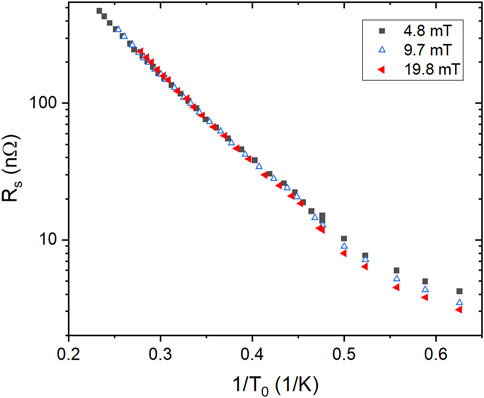
Figure 1. Rs(T0) measured for different Bp-values after the first cool-down.
Figure 2 shows a plot of Q0(Bp) measured at 1.6 K in two consecutive cavity tests. The first test was performed after the first cool-down described in Section 2.1. The second test was performed after warming up the cavity to 80 K followed by a cool-down at a faster rate of ∼5 K/min, resulting in a larger temperature gradient of
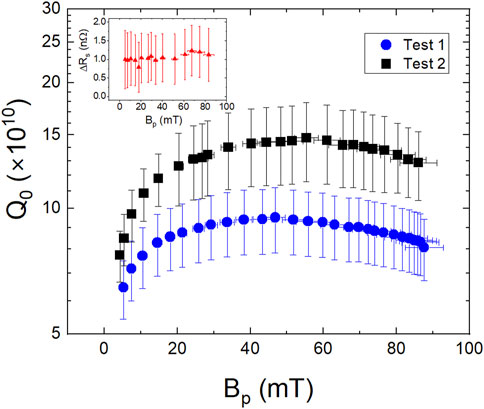
Figure 2. Q0(Bp) measured at 1.6 K after ∼1.5 K/min (Test 1) and ∼5 K/min (Test 2) cool-down rates across Tc. The inset shows the Rs-difference between Test 1 and Test 2 as a function of Bp.
The cavity performance was limited in both tests by a quench at Bp ∼ 86 mT, without any field emission. The temperature maps measured just below the quench field are shown in Figure 3. The Q0 at 1.6 K degraded by
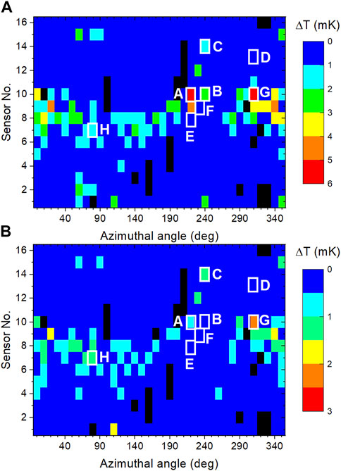
Figure 3. Unfolded temperature maps measured at 1.6 K and Bp ∼84 mT during Test 1 (A) and Test 2 (B) before quench. Sensor No. 8 is at the equator, No. 1 is at the bottom iris and No. 16 at the top beam tube, close to the iris. The location of the cut-out samples, labelled A-H are highlighted in white. Faulty sensor locations are shown in black.
The quench location was the same in both tests, at temperature sensor No. 10 at the azimuthal angle of 220°. This location is
Figure 4 shows the local temperature difference ΔT(Bp) between the cavity outer surface and the He bath at the location of the samples A-H, measured after Tests 1 and 2. The estimated combined systematic and statistical uncertainty in the temperature measurement is ∼1 mK. The magnitude of ΔT(Bp) at the hot-spot locations dropped significantly after Test 2. An increase in ΔT(Bp) was found at the location of sample A, for both tests, and of sample B for Test 2, after multiple quench events at the highest rf field. Hysteretic behavior of ΔT(Bp) at some locations of a different N-doped SRF cavity was also reported in Ref. (Makita et al., 2015). The losses at the hot-spot locations can be characterized with a power law,
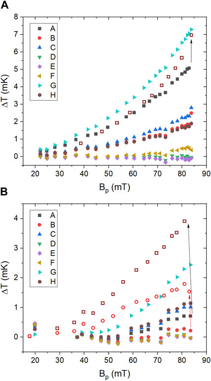
Figure 4. ΔT(Bp) measured at 1.6 K during Test 1 (A) and Test 2 (B) at the 8 locations chosen for cutouts. The empty symbols were measured at sample locations A and B while decreasing the RF field after quench, showing a hysteretic behavior. In the case of sample B, hysteretic behavior occurred only during Test 2.
The samples used for XPS, STM and SEM characterization were cut from the cavity using a computer numerical control milling machine with no lubricant. During the cutting process, the samples were cooled by using a steady flow of compressed helium gas at the milling location. During the milling process the samples temperature did not raise above 32°C. To ensure that the cutting process did not change the sample, a time-of-flight secondary ion mass spectrometry analysis was performed on a 16 × 16 mm2 sample, and the measurements were repeated near the same location after cutting out an 8 × 8 mm2 sample. After the milling, an increase in carbon was found but new impurities were not. Table 1 shows the sequence of analysis done for each sample. The results from the XPS analysis of sample B and from the STM analysis of samples D and E have been previously reported in Ref. (Lechner et al., 2020).
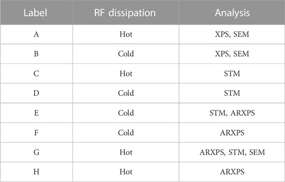
Table 1. Surface characterization sequence for all of the samples cut from the N-doped Nb cavity, listed in the order in which they were performed.
A PHI Versaprobe 5000 XPS at the Drexel University Core Facilities was used for XPS measurements. The X-ray source used was Al K α (1486.6 eV, 200 W). The binding energy was calibrated to the adventitious carbon C 1 s peak, corresponding to C-C bonds, at 284.6 eV. The depth profile was performed using Ar ion sputtering at 1 keV, 2 μA beam current and 2 mm × 2 mm beam size. We estimated a sputtering rate of 1.1 nm/min by atomic force microscopy (AFM).
The surface oxidation of Nb has been previously studied using XPS (Grundner and Halbritter, 1984; Hu et al., 1989; King et al., 1990), ultraviolet photoemission (Lindau and Spicer, 1974), Auger electron spectroscopy (Farrell et al., 1973; Franchy et al., 1996) and high-resolution electron energy loss spectroscopy (Franchy et al., 1996). These investigations have shown that NbO and NbO2 are initially formed on Nb, with Nb2O5 being formed after further oxidation (Lindau and Spicer, 1974; Grundner and Halbritter, 1984; Hu et al., 1989; King et al., 1990; Franchy et al., 1996). The oxidation state of Nb can be changed substantially after annealing in ultra-high vacuum or sputtering where Nb2O5 is reduced to NbO2 and NbO due to the dissolution of O into the bulk (King et al., 1990; Lechner et al., 2021).
We studied the surface of hot-spot sample A and cold-spot sample B. A lower resolution survey was used to get information about the elements present on the surface. High resolution scans around peaks corresponding to the elements of interest were then performed to obtain the fine structure of the peaks, which contain the information about the chemical environment. In the survey spectrum of both samples there are visible peaks for O 1s, Nb 3d, Nb 3p, Nb 3s, Nb 4s and carbon C 1s. The signal for the N 1s is not detectable in this low energy resolution spectrum.
High resolution XPS spectra for Nb 3d was carried out within 200–216 eV. The Nb 3d core level of the native surface of sample A (hot) and B (cold) showed slightly higher peaks for Nb2O5 for sample A. The Nb 3d peaks can be summarized as follows: Nb5+ (Nb2O5) peaks are located at 210.0 eV and 207.3 eV, Nb4+ (NbO2) peaks are located at 208.8 eV and 206.0 eV, Nb2+ (NbO) peaks are located at 206.8 eV and 204.0 eV and Nb0 peaks are at 205.0 eV and 202.2 eV (King et al., 1990). Numerous oxygen vacancies exist in Nb2O5 (Grundner and Halbritter, 1984; Halbritter, 1987; Proslier et al., 2011). Therefore, the Nb2O5 peaks are comprised of Nb2O5 and O-deficient Nb2O5 which makes it difficult to distinguish between the two from XPS spectra (Ohsawa et al., 2011).
Although the oxidation states of metals can be altered by Ar ion bombardment (Hashimoto and Tanaka, 2002), qualitative comparison between hot and cold-spots subjected to the same procedure can provide useful insight into the material science of the surface. It has been shown that Ar ion sputtering of oxidized Nb removes oxygen preferentially from Nb2O5 and diffuses it into the bulk, which tends to thicken the lower oxidation state layers (Karulkar, 1981). However, the ion current density used for the study in Ref (Karulkar, 1981). is more than three orders of magnitude greater than the one we used, therefore we may expect less of a change in the oxide composition during Ar ion sputtering in our study.
Figure 5 shows the evolution of the Nb 3d spectral lines during Ar ion sputtering. The depth profile shown in Figure 5 reveals that sample A does not retain the higher oxides and reverts to the Nb0 bulk relatively quickly compared to sample B that instead retains the higher oxide states.
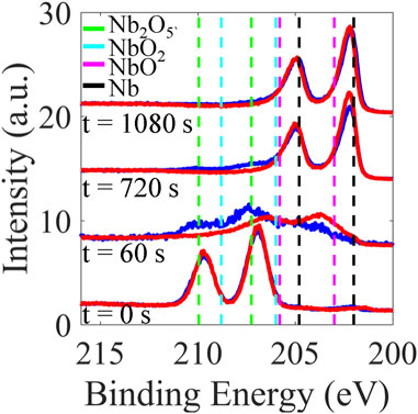
Figure 5. Evolution of the Nb 3d lines spectra acquired during depth profiling of hot-spot sample A (red) and cold-spot sample B (blue). From bottom to top, the XPS spectra were taken after sputtering times of 0 s, 60 s, 720 s, and 1080 s, showing larger spectral weight for higher oxidation states in the cold spot while the hot-spot has a larger weight of low oxides, NbOx around ∼ 203–204 eV especially near the surface. The Nb 3d3/2 and Nb 3d5/2 peaks of various oxidation states are shown with vertical dashed lines.
In order to investigate the thickness of the native oxide and suboxides, ARXPS measurements were made with a PHI Quantera SXM-03 XPS at Virginia Tech’s Nanoscale Characterization and Fabrication Laboratory. Samples E-H were rinsed with reagent grade ethanol and mounted in the XPS chamber by conductive carbon tape at the same time. Each was sputtered with 1 keV Ar for 30 s to remove surface carbon contamination, improving the signal-to-noise ratio for measuring the Nb 3d lines. The x-ray beam from the monochromator was focused to a 100 μm spot. For the variable angle data, at each position full survey scans were collected as 15 sweeps with pass energy set to 280 eV and step size at 1 eV. Measurements were taken at 15°–90° angles at 15° increments. No significant difference was found among the 4 samples from the angle-resolved XPS spectra.
High resolution Nb 3d scans consisting of 20 sweeps with 13 eV pass energy and 0.025 eV step size were collected at 45° take-off angle for each sample. The XPS curve fitting was performed in CasaXPS using a Shirley background and Gaussian-Lorentzian, GL (30), line shapes to determine chemical state and their contribution to the measured signal. The spin orbit splitting was taken as 2.72 eV and the ratio of intensities for the split lines was 2/3 (Chastain and King, 1992). Nb 3d spectra could be fit satisfactorily using three oxidation states, Nb2O5, NbO2, NbOx where x =0.4–0.6 (Prudnikava et al., 2022), and Nb. Thicknesses of different oxide components were determined using the multilayer model (Darlinski and Halbritter, 1987)
where subscript u represents the substrate, λi is the inelastic mean free path of layer i, θ is the electron take-off angle, ni is the atomic density of the detected species and Fi is the spectral area of the signal related to layer i. Ti is the transmission coefficient which accounts for the attenuation through the preceding overlayer by Ti = exp(−di/λi cos θ). Values of the inelastic mean free path were estimated using the TPP-2M formula (Tanuma et al., 1994) and atomic densities were taken from (Halbritter, 1987). The estimated thickness of the oxide components are listed in Table 2. More in-depth analysis have been performed in the NbOx system (Lubenchenko A. et al., 2018; Lubenchenko AV. et al., 2018) which show that the Shirley background and Gaussian-Lorentzian line shapes have a thickness uncertainty of
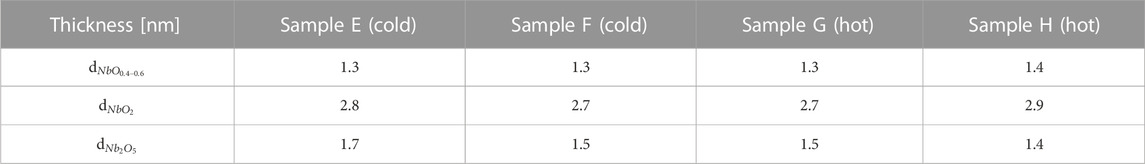
Table 2. Thickness of the Nb oxides for samples E-H, determined from the deconvolution of the Nb 3d spectral lines measured by XPS at a 45° take-off angle.
A FEI Quanta 450 FEG SEM was used for microscopy study of the rf surface of the cutout samples. The SEM images did not show any evidence for either niobium nitride or hydride features left on the surface. This is somewhat expected since it has been shown that nitrides are removed from the surface by 5 − 10 μm EP and that most of the hydrogen is degassed from the Nb by the 800°C vacuum annealing. Any residual hydrides have the size of a few nanometers, requiring high-resolution transmission electron microscopy to reveal them. The presence of a grain boundary was a distinctive feature observed on both samples A and G. The grain boundary found in sample A is shown in Figure 6.
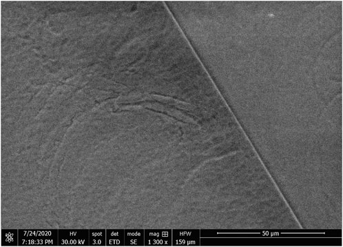
Figure 6. SEM image of sample A at 1300x magnification.
A Unisoku ultra-high vacuum STM system equipped with a 9 T superconducting magnet and with a base pressure of 4 × 10⁻¹¹ Torr was used to perform low temperature scanning tunneling microscopy/spectroscopy (STM/STS) measurements between 1.0 K to 1.5 K. Pt-Ir tips prepared on Au were used in all measurements. The samples used for STM measurements are cold (Sample D) and hot (Sample C and G) spot cutouts from the same N-doped Nb cavity. Since the surface of Nb is dominated by a layer of a dielectric oxide Nb2O5, which is too thick to tunnel through, it is necessary to remove the dielectric layer by Ar ion sputtering. These samples were sputter-cleaned in a UHV sample preparation chamber attached to the STM chamber with a base pressure of low 10−11 Torr. Ar ion sputtering was performed using 99.999% pure Ar at a pressure of 10−5 Torr and accelerating voltage of 1 kV for 1 h with a 4.75 μA beam current and 10 mm × 10 mm beam size. The removal rate was 0.27 nm/min as estimated by atomic force microscopy on a calibration sample. The Ar sputtering process removes the surface pentoxide and yields a metallic oxide surface NbOx a few nm thick. This surface can be studied by STM that allows to study the local superconducting properties of the material. Clean and metallic surfaces are suitable for STM studies of local tunneling spectra as well as imaging of vortices, which leads to an estimate of the coherence length and mean free path. All differential conductance (dI/dV) measurements were made with the same tunneling parameters. The junction was stabilized at V = 10 mV, I = 60 pA and a standard lock-in technique was used with Vmod = 200 μV at 373.1 Hz.
Tunneling spectra were acquired on cold and hot-spots N-doped Nb cutouts and analyzed in the framework of a proximity-coupled model which describes a thin metallic suboxide layer on the surface of a bulk superconductor (Gurevich and Kubo, 2017). We used the fitting procedure described in detail in (Gurevich and Kubo, 2017; Lechner et al., 2020) to extract the density of states at the surface N(E) from the tunneling spectra. The so-obtained N(E) depends on the Dynes broadening parameter Γ (Dynes et al., 1978) and two dimensionless parameters α and β, proportional to the thickness of the normal layer d and the contact resistance RB between the normal layer and the superconductor:
Here,
Typical tunneling conductance spectra are shown in Figures 7A, B for samples D and C, respectively. The overall shape of these spectra, for cold and hot-spots, differs significantly in the subgap region and in the shape and height of the coherence peak. Tunneling spectra were acquired on grids with a spacing of 32.6 nm over areas of 391 nm × 391 nm and 781 nm × 781 nm. Analysis of these spectra shows that the average Δ0 is lower by 1% − 2% in the hot-spot samples compared to the cold-spot one. Furthermore, histograms of the extracted fit parameters clearly show that hot-spots have wider distributions of α, β, Γ, Δ0 than the cold-spot. For instance, there is a low Δ0 tail in the gap distribution in sample G, as shown in Figure 7C, where the low Δ0 values have been magnified to show the difference between cold and hot-spots. The number of tunneling spectra acquired for sample D was 576, that for sample C was 720 and that of sample G was 1108. The Dynes broadening parameter Γ is found to be higher, on average, in the hot-spot samples as supported by the wider distribution for samples C and G, presented in Figure 7D. The α-distribution, shown in Figure 7E, reveals that hot-spots are more likely to have larger normal layers which tend to be detrimental and enhance the surface resistance (Gurevich and Kubo, 2017). The parameter β (Figure 7F) in sample G exhibits a significant spread away from an optimum value of 0.3–0.4 at which a minimum in the surface resistance is predicted to occur (Gurevich and Kubo, 2017).
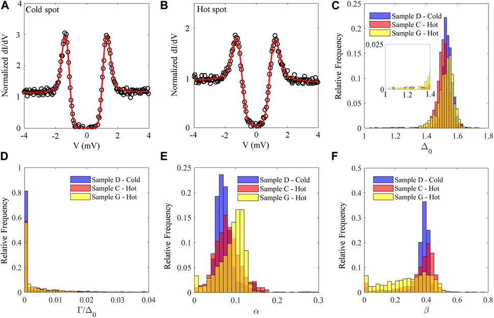
Figure 7. (A,B) Representative spectra for cold-spot sample D and hot-spot sample C from a N-doped Nb cavity. The red curves are the fit obtained using the proximity effect theory (Gurevich and Kubo, 2017) and described in the text. The fitting parameters in (A) are: Δ0 = 1.56 meV, Γ =0 meV, α = 0.08, β = 0.39, T =1.17 K. The fitting parameters in (B) are: Δ0 = 1.51 meV, Γ =0.03 meV, α =0.14, β = 0.04, T = 1.45 K. The results of the fitting procedure for all tunneling spectra acquired on cold and hot spot samples between 1.0 K and 1.5 K are summarized in the histogram comparison for the fit parameters Δ0, Γ/Δ0, α, and β reported in (C–F). In panel (C) the low Δ0 values are shown magnified by a factor 10 to better visualize the difference between cold and hot spot results.
STM grids on all samples investigated, also reveal the presence of near-surface defects that induce in-gap states in the quasiparticle density of states. Measurements of hot-spot samples C and G reveal a significantly higher density of such defects. Example of these spectra are shown in Figure 8 where a line of spectra has been acquired along one of these extended defects on sample G. Zero-bias peaks and in-gap states in the quasiparticle density of states could indicate the presence of magnetic impurities (Proslier et al., 2011) possibly associated with Nb suboxides (Cava et al., 1991).
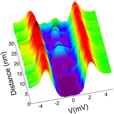
Figure 8. A line of 100 tunneling spectra acquired across an extended defect on hot-spot sample G. In all spectra the tip is stabilized at Vset =10 mV, Iset =60 pA, and the lock-in bias modulation Vmod =0.20 mV is used.
To estimate the coherence length ξs and the mean free path l, a perpendicular magnetic field was applied to the sample’s surface to generate Abrikosov vortices that modify the local density of states in the vortex core of ≃ 2ξs in diameter. Vortices were imaged using STM by mapping the conductance at an energy where a vortex alters the density of states. Figures 9A, B show the vortex lattice, imaged by acquiring the density of states at the Fermi energy, on cold-spot sample D and hot-spot sample C. Both samples show a triangular vortex lattice consistent with theoretical predictions (Blatter et al., 1994; Brandt, 1995). Superconductors in the superclean limit, l ≫ ξ0, exhibit the Caroli-de Gennes-Matricon bound states localized in the vortex core (Caroli et al., 1964; Hess et al., 1989; Renner et al., 1991), but those are not found here, indicating that the samples are in the dirty limit, l < ξ0, where ξ0 is the coherence length in the absence of impurities. Spatial analysis of the conductance around vortices
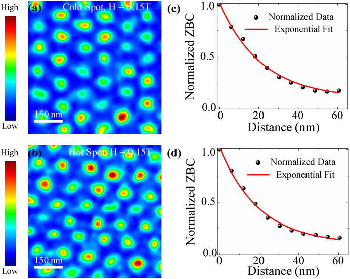
Figure 9. Normalized zero-bias conductance image showing vortices at T = 1.5 K and H = 0.15 T in N-doped Nb cold-spot D (A) and in the N-doped Nb hot-spot C (B). The scan area for both images is 697 nm × 697 nm and the magnetic field was applied normal to the surface. (C,D) Normalized zero bias conductance plotted as a function of distance from the vortex center for the cold and hot spot respectively. The solid lines are exponential fits to extract the coherence length. In all vortex images the tip is stabilized at Vset =10 mV, Iset =60 pA, and the lock-in bias modulation Vmod =0.20 mV is used.
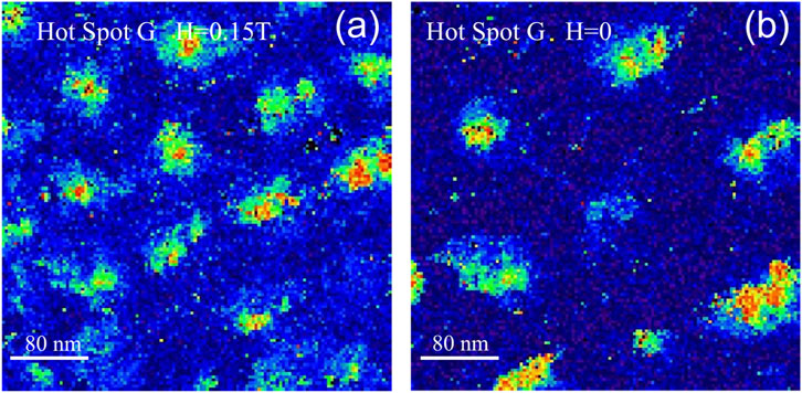
Figure 10. Normalized zero-bias conductance image showing vortices at T = 1.5 K and H = 0.15 T in N-doped Nb hot spot Sample G. (A) Field-cooled image at H = 0.15 T. (B) Conductance image of the same area after removal of the field without increasing the temperature (H = 0). The scan area for both images is 391 nm × 391 nm and the magnetic field was applied normal to the surface. The tip is stabilized at Vset =10 mV, Iset =60 pA, and the lock-in bias modulation Vmod = 0.20 mV is used.
STM vortex images of sample G show strong pinning and a distorted vortex lattice. Figure 10A shows a field-cooled vortex image taken at H = 0.15 T. Figure 10B shows instead an image of the same area after removal of the field without increasing the temperature. The image shows that vortices are trapped. Zero-field cooled images show absence of vortices in this area located approximately at the center of the sample. High resolution single vortex images have been used to determine the coherence length on sample G and yield a value of ξs≅ (20 ± 2) nm. The strong pinning found in this sample could explain the persistent excess RF dissipation found by T-mapping after both slow and fast cooldown.
Our combined temperature mapping and scanning tunneling experiments have shown a complex interplay of both surface and bulk sources of RF losses in hot-spots. The temperature mapping has shown that both the intensity of hot-spots and their spatial distribution depends strongly on the cool-down rate of the cavity. This observation clearly demonstrates a significant contribution of trapped vortices to RF losses in hot spots. At the same time, our analysis of STM/STS and XPS experimental data has shown that hot-spots regions exhibit weakly degraded superconducting properties at the surface with a wider distribution of superconducting gaps and a noticeable fraction of low-Δ regions.
A challenge common to all of the experimental studies found in the literature in which cavity cutout samples, identified by temperature mapping, have been analyzed by surface analytical methods is the difference between the spatial resolution of the thermometer and the size of area probed by surface analysis tools. The size of the thermometer used for temperature mapping is
XPS measurements have revealed that the N-doped hot-spot exhibits lower oxidation states of Nb deeper into the surface which may be the cause of a degraded interface resistance. The analysis of the STM spectra have shown that hot-spots may have a thicker normal suboxide and a non-optimum contact resistance between the suboxide and the bulk Nb. The hot-spot also suffers from a degraded Δ0 with a fraction of particularly low Δ0 regions which can significantly increase local RF losses. Moreover, the Dynes parameter Γ/Δ0 turns out to be larger in the hot-spot, indicating stronger Cooper pairbreaking and larger surface resistance (Gurevich and Kubo, 2017). Yet our STM imaging of vortex cores shows that the electron mean free path is nearly the same in hot and cold-spots.
We used the model of a proximity-coupled normal layer on the surface of a bulk superconductor, which describes well the tunneling spectra, to calculate Rs(T) with the parameters α, β, Γ and Δ0 obtained from fitting the STM data (Gurevich and Kubo, 2017). Additional parameters in the model are the electrons’ mean free path, the resistivity of the normal layer, ρn, and the Debye energy, Λ = 23.6 meV, the latter taken as a material constant. l = 6.2 nm was obtained from a least-squares fit of Rs(T0) at 4.8 mT with Rs(T) = RBCS(T) + Ri, where RBCS(T) is the low-field Mattis-Bardeen surface resistance calculated numerically with Halbritter’s code (Halbritter, 1970). λ0 = 32 nm, ξ0 = 39 nm and Tc = 9.25 K were considered material constants for clean Nb and the mean value
The RF penetration depth and bulk coherence length used in the calculation of Rs(T) with the proximity-coupled normal layer model were
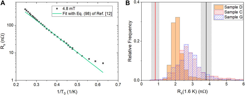
Figure 11. (A) Average cavity surface resistance as a function of LHe bath temperature, measured at 4.8 mT during Test 1 and Rs(T) calculated with the model of Ref (Gurevich and Kubo, 2017). with the average parameters from cold spot D, l = 6.2 nm and ρn = 0.5 μΩcm. The size of the error bars are about the same size of the symbols. (B) Histograms of Rs(1.6 K) calculated with the model of Ref. (Gurevich and Kubo, 2017) for each set of parameters α, β, Γ, Δ0 from the STM data for samples C, D and G. The solid black line is Rs(1.6 K) measured during Test 2, the solid red line is RBCS(1.6 K) and the gray shaded areas represent ± 1σ.
Following the same approach described above, we calculated Rs at 1.6 K for each set of parameters α, β, Γ and Δ0 obtained from the STM data for cold-sample D and hot-spot samples C and G, resulting in the histograms shown in Figure 11B. The median, mean and standard deviation from each sample are listed in Table 3. The median value of Rs(1.6 K) is
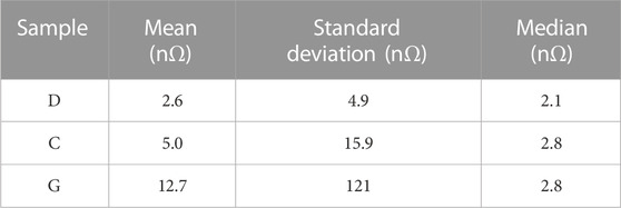
Table 3. Statistics on the surface resistance at 1.6 K calculated from the model of Ref (Gurevich and Kubo, 2017). for a proximity-coupled normal layer, using the model parameters obtained from STM data for samples C (hot-spot), D (cold-spot) and G (hot-spot).
The contribution to the surface resistance at 1.6 K from the ideal BCS theory is (0.8 ± 0.2) nΩ, therefore the proximity-coupled normal layer contributes
where H0 is the local surface RF magnetic field and η is the thermometers’ efficiency. η = 0.53 K cm2/W was obtained by a linear least-squares fit of ΔT, averaged over the outer surface, versus the RF power density. The local Rs at 80 mT at the locations of samples C and G was (8.8 ± 0.3) nΩ and (20.4 ± 0.6) nΩ for Test 2, respectively. Even higher local Rs-values were obtained at those locations during Test 1. These results clearly show that the additional RF dissipation in those hot spot locations is due to trapped vortices. This conclusion is consistent with the Arrhenius plot in Figure 11A which shows that the observed global residual resistance is higher than the prediction of the proximity model with the Dynes pairbreaking. This extra residual resistance is naturally produced by trapped vortices.
To evaluate the bulk and surface contributions to RF losses we use the following relation between the excess power P0 in a hot-spot at the inner cavity surface and the resulting maximum value of ΔT observed by the temperature mapping on the outer cavity surface (Gurevich and Ciovati, 2013):
Here a hot-spot has a lateral size
Using Eq. 4 we evaluate the number of vortices N which can produce the observed values of ΔT shown in Figure 3. Here the power P0 generated by N sparse vortices under RF field at GHz frequencies f is given by (Gurevich and Ciovati, 2013):
where ρs is the normal state resistivity of Nb. Taking w = 2.8 mm, κ ≈ 7 W/mK, hK ≈ 2.5 kW/m2K at T = 1.6 K, we obtain the thermal length Lh ≃ 2.8 mm which defines the spatial scale of temperature spreading along the cavity surface from a local heat source. For f = 1.3 GHz, Bp = 83 mT, ρs ≃ 7 × 10⁻⁸ Ω m, and λ/ξs ∼ λ0/l ≃ 4 given by STM of vortices shown in Figure 9, we obtain from Eqs 4, 5 that N ∼ 8 × 10² − 2 × 10³ for ΔT ≃ 2 − 5 mK in Test 1 and N ∼ 400 for ΔT ≃ 1 mK in Test 2. Assuming that trapped vortices are spaced by ∼ λ ≃ 80 nm, we estimate sizes of vortex bundles as
Another contribution to RF losses could come from the weakly deteriorated superconducting properties at the surface revealed by our STM measurements. Here the extra power
where Pi is a fraction of the hot spot area where α, β, Δ take particular values according to the histograms shown in Figure 7, and the last term in Eq. 6 describes the BCS surface resistance RBCS for an ideal surface in the cold-spot areas. The pre-factor Ri(αi, βi, Δi) in Eq. 6 is a rather complicated function of the parameters (Gurevich and Kubo, 2017; Kubo and Gurevich, 2019), so we only make here a rough estimate of the size L of a surface hot-spot which could provide the observed ΔT values shown in Figure 3.
The reduction of the mean gap value from Δ0 ≈ 1.55 meV in cold spots to ⟨Δ⟩ ≈ 1.5 meV in hot-spots shown in Figure 7 increases Rs by the factor
For ΔT = 1 mK, Bp = 83 mT and the above values of other parameters, Eq. 7 yields L ≃ 3 mm, more than 2 orders of magnitude larger than the size of the vortex hot-spots causing ΔT = 1 mK. Thus, the changes in the surface superconducting properties revealed by STM give much weaker contributions to the observed temperature maps than trapped vortices. Yet our STM/STS measurements revealed a clear correlation between the weakly deteriorated superconducting properties at the surface and the positions of the hot-spots identified by temperature mapping. Moreover, the severity of the deterioration correlates with the inability to expel flux from that region during cool-down, as shown by the results from STM and T-maps on sample G. We suggest that, although the observed changes in the properties of the oxide layer and superconducting gap are not the prime sources of the RF power in the hot-spot sample, these parts of the cavity may be the regions where vortices first nucleate and then get trapped by bulk pinning centers upon cooling of the cavity through Tc. Another mechanism by which a reduced gap in hot-spots can be linked with trapped vortices may result from subsurface metallic nanohydrides (Yang et al., 2019; Veit et al., 2020). Due to the proximity effect (Tinkham, 2004), such metallic nanoparticles locally reduce Δ(T) over distances ∼ ξs around them. As a result, the nanoparticles that are closer than a few ξs to the surface not only can pin vortices but also cause a shadow effect of reduced Δ at the surface observed by STM.
The exponent n > 2 in the overheating ΔT ∝ Hn can result from a temperature dependence of the surface resistance Rs(T), even if Rs containing both the BCS and vortex contributions is independent of H. This follows from the uniform thermal balance equation YΔT = Rs(T)H2/2 which shows that ΔT(H) increases faster than H2 if Rs(T) increases with T. Here Y is the thermal conductance of the cavity wall (Gurevich, 2012).
The local overheating at the quench spot measured after the two cool-downs is fairly weak. Weak overheating in a small flux hot-spot is proportional to the power in the hot-spot but the thermal breakdown field remains close to the uniform breakdown field without the hot-spot (Gurevich, 2012; Gurevich and Ciovati, 2013). The origin of the reduced quench field in N-doped cavities is not entirely clear. The average quench field changes with the duration of the N-exposure and of the post-annealing (Gonnella et al., 2018; Maniscalco et al., 2022). In addition to geometric magnetic field enhancement at grain boundaries and topographic defects, the reduction of the breakdown field of N-doped cavities can result from a dirtier surface, which reduces both the lower critical field Hc1 and Hs because the Ginzbug-Landau (GL) parameter κ = λ/ξ increases as the mean free path decreases. For instance,
Regions with different RF loss characteristics were located with thermometry mapping during the RF test of a N-doped Nb cavity. The cavity performance was limited by a quench at 86 mT and the quench location was the same after both slow and fast cool-down. A grain boundary was found at the quench location.
Cutouts from hot-spot regions were characterized by XPS and STM/STS measurements. The STM results can be described by a model which includes a thin proximity-coupled normal layer on top of the superconductor, resulting in a small degradation of both superconducting gap and degraded interface resistance in hot-spot regions, compared to cold-spot ones. The model parameters obtained from the STM measurements were used to calculate a distribution of Rs-values at 1.6 K. The thickness of the normal layer was estimated to be of the order of 1 nm, contributing by
Our analysis of the experimental data suggests that weakly degraded superconducting properties at the surface of hot-spot regions are not the main source of RF losses, rather they are regions where vortices settle during cool-down. Vortex nucleation may also be preferential in theses locations but nucleation could also be facilitated by grain boundaries (Balachandran et al., 2021), such as found on samples A and G. While stronger thermal gradients will enhance flux expulsion, as shown in Figure 3, poorly superconducting regions remain vulnerable to preferentially trapping vortices.
The raw data supporting the conclusion of this article will be made available by the authors, without undue reservation.
MI, GC, and AG contributed to conception and design of the study. MI, EL, and BO did the STM, XPS, and SEM measurements and data analysis. JM did the RF and thermometry measurements and data analysis. GC and AG contributed to the data analysis. MI and EL wrote the first draft of the manuscript. GC and AG wrote sections of the manuscript. All authors contributed to the article and approved the submitted version.
This work was supported by the National Science Foundation, under award PHY-1734075. Some of the calculations were carried out on Temple University’s HPC resources supported in part by the National Science Foundation through major research instrumentation grant no. 1625061 and by the US Army Research Laboratory under contract number W911NF-16-2-0189. GC is supported by Jefferson Science Associates, LLC under U.S. DOE Contract No. DE-AC05-06OR23177. The work of JM and AG at Old Dominion University was supported by DOE under grant DE-SC 100387-020.
The authors would like to acknowledge the use of the Core Facility at Drexel University for the XPS measurements, the Nano Instrumentation Center and Dmitriy A. Dikin at Temple University for the SEM measurements. The authors would also like to acknowledge M. Kelley and W. Leng for the ARXPS measurements at Virginia Tech.
The authors declare that the research was conducted in the absence of any commercial or financial relationships that could be construed as a potential conflict of interest.
All claims expressed in this article are solely those of the authors and do not necessarily represent those of their affiliated organizations, or those of the publisher, the editors and the reviewers. Any product that may be evaluated in this article, or claim that may be made by its manufacturer, is not guaranteed or endorsed by the publisher.
Antoine, C. (2012). “Materials and surface aspects in the development of SRF niobium cavities,”. Report No:EuCARD-BOO-2012-001 (Paris: CEA Saclay). Tech. Rep.
Aune, B., Bandelmann, R., Bloess, D., Bonin, B., Bosotti, A., Champion, M., et al. (2000). Superconducting TESLA cavities. Phys. Rev. St. Accel. Beams 3, 092001. doi:10.1103/PhysRevSTAB.3.092001
Balachandran, S., Polyanskii, A., Chetri, S., Dhakal, P., Su, Y. F., Sung, Z. H., et al. (2021). Direct evidence of microstructure dependence of magnetic flux trapping in niobium. Sci. Rep. 11, 1–12. doi:10.1038/s41598-021-84498-x
Barkov, F., Romanenko, A., Trenikhina, Y., and Grassellino, A. (2013). Precipitation of hydrides in high purity niobium after different treatments. J. Appl. Phys. 114, 164904. doi:10.1063/1.4826901
Blatter, G., Feigel’man, M. V., Geshkenbein, V. B., Larkin, A. I., and Vinokur, V. M. (1994). Vortices in high-temperature superconductors. Rev. Mod. Phys. 66, 1125–1388. doi:10.1103/RevModPhys.66.1125
Brandt, E. H. (2003). Properties of the ideal Ginzburg-Landau vortex lattice. Phys. Rev. B 68, 054506. doi:10.1103/PhysRevB.68.054506
Brandt, E. H. (1995). The flux-line lattice in superconductors. Rep. Prog. Phys. 58, 1465–1594. doi:10.1088/0034-4885/58/11/003
Caroli, C., De Gennes, P., and Matricon, J. (1964). Bound Fermion states on a vortex line in a type II superconductor. Phys. Lett. 9, 307–309. doi:10.1016/0031-9163(64)90375-0
Casalbuoni, S., Knabbe, E., Kötzler, J., Lilje, L., von Sawilski, L., Schmüser, P., et al. (2005). Surface superconductivity in niobium for superconducting rf cavities. Nucl. Instrum. Methods Phys. Res. Sect. A Accel. Spectrom. Detect. Assoc. Equip. 538, 45–64. doi:10.1016/j.nima.2004.09.003
Cava, R. J., Batlogg, B., Krajewski, J. J., Poulsen, H. F., Gammel, P., Peck, W. F., et al. (1991). Electrical and magnetic properties of Nb2O5−δ crystallographic shear structures. Phys. Rev. B 44, 6973–6981. doi:10.1103/PhysRevB.44.6973
Chastain, J., and King, R. C. (1992). Handbook of x-ray photoelectron spectroscopy. Perkin-Elmer Corp. 40, 221.
Ciovati, G., Dhakal, P., and Gurevich, A. (2014). Decrease of the surface resistance in superconducting niobium resonator cavities by the microwave field. Appl. Phys. Lett. 104, 092601. doi:10.1063/1.4867339
Ciovati, G., Dhakal, P., and Myneni, G. R. (2016). Superconducting radio-frequency cavities made from medium and low-purity niobium ingots. Supercond. Sci. Technol. 29, 064002. doi:10.1088/0953-2048/29/6/064002
Ciovati, G., and Gurevich, A. (2008). Evidence of high-field radio-frequency hot spots due to trapped vortices in niobium cavities. Phys. Rev. St. Accel. Beams 11, 122001. doi:10.1103/PhysRevSTAB.11.122001
Ciovati, G., and Gurevich, A. (2007). “Measurement of RF losses due to trapped flux in a large-grain niobium cavity,” in Proc. SRF’07, Beijing, China, October 2007 (Geneva, Switzerland: JACoW Publishing), 132–136.
Ciovati, G. (2005). Investigation of the superconducting properties of niobium radio-frequency cavities. Norfolk, VA: Old Dominion University.
Dangwal Pandey, A., Dalla Lana Semione, G., Prudnikava, A., Keller, T. F., Noei, H., Vonk, V., et al. (2018). Surface characterization of nitrogen-doped Nb (100) large-grain superconducting RF cavity material. J. Mater. Sci. 53, 10411–10422. doi:10.1007/s10853-018-2310-8
Darlinski, A., and Halbritter, J. (1987). Angle-resolved XPS studies of oxides at NbN, NbC, and Nb surfaces. Surf. Interface Analysis 10, 223–237. doi:10.1002/sia.740100502
Dhakal, P., Chetri, S., Balachandran, S., Lee, P. J., and Ciovati, G. (2018). Effect of low temperature baking in nitrogen on the performance of a niobium superconducting radio frequency cavity. Phys. Rev. Accel. Beams 21, 032001. doi:10.1103/PhysRevAccelBeams.21.032001
Dhakal, P., Ciovati, G., and Gurevich, A. (2020). Flux expulsion in niobium superconducting radio-frequency cavities of different purity and essential contributions to the flux sensitivity. Phys. Rev. Accel. Beams 23, 023102. doi:10.1103/PhysRevAccelBeams.23.023102
Dhakal, P., Ciovati, G., Myneni, G. R., Gray, K. E., Groll, N., Maheshwari, P., et al. (2013). Effect of high temperature heat treatments on the quality factor of a large-grain superconducting radio-frequency niobium cavity. Phys. Rev. St. Accel. Beams 16, 042001. doi:10.1103/PhysRevSTAB.16.042001
Dhakal, P., Ciovati, G., Pudasaini, U., Chetri, S., Balachandran, S., and Lee, P. J. (2019). Surface characterization of nitrogen-doped high purity niobium coupons compared with superconducting rf cavity performance. Phys. Rev. Accel. Beams 22, 122002. doi:10.1103/PhysRevAccelBeams.22.122002
Dhakal, P. (2020). Nitrogen doping and infusion in SRF cavities: A review. Phys. Open 5, 100034. doi:10.1016/j.physo.2020.100034
Dynes, R. C., Narayanamurti, V., and Garno, J. P. (1978). Direct measurement of quasiparticle-lifetime broadening in a strong-coupled superconductor. Phys. Rev. Lett. 41, 1509–1512. doi:10.1103/PhysRevLett.41.1509
Farrell, H., Isaacs, H., and Strongin, M. (1973). The interaction of oxygen and nitrogen with the niobium (100) surface: II. reaction kinetics. Surf. Sci. 38, 31–52. doi:10.1016/0039-6028(73)90272-0
Franchy, R., Bartke, T., and Gassmann, P. (1996). The interaction of oxygen with Nb(110) at 300, 80 and 20 K. Surf. Sci. 366, 60–70. doi:10.1016/0039-6028(96)00781-9
Garfunkel, M. P. (1968). Surface impedance of Type-I superconductors: calculation of the effect of a static magnetic field. Phys. Rev. 173, 516–525. doi:10.1103/PhysRev.173.516
Garg, P., Balachandran, S., Adlakha, I., Lee, P. J., Bieler, T. R., and Solanki, K. N. (2018). Revealing the role of nitrogen on hydride nucleation and stability in pure niobium using first-principles calculations. Supercond. Sci. Technol. 31, 115007. doi:10.1088/1361-6668/aae147
Gonnella, D., Aderhold, S., Burrill, A., Daly, E., Davis, K., Grassellino, A., et al. (2018). Industrialization of the nitrogen-doping preparation for SRF cavities for LCLS-II. Nucl. Instrum. Methods Phys. Res. Sect. A Accel. Spectrom. Detect. Assoc. Equip. 883, 143–150. doi:10.1016/j.nima.2017.11.047
Gonnella, D., Eichhorn, R., Furuta, F., Ge, M., Hall, D., Ho, V., et al. (2015). Nitrogen-doped 9-cell cavity performance in a test cryomodule for LCLS-II. J. Appl. Phys. 117, 023908. doi:10.1063/1.4905681
Grassellino, A., Romanenko, A., Sergatskov, D., Melnychuk, O., Trenikhina, Y., Crawford, A., et al. (2013). Nitrogen and argon doping of niobium for superconducting radio frequency cavities: A pathway to highly efficient accelerating structures. Supercond. Sci. Technol. 26, 102001. doi:10.1088/0953-2048/26/10/102001
Groll, N., Ciovati, G., Grassellino, A., Romanenko, A., Zasadzinski, J., and Proslier, T. (2018). Insight into bulk niobium superconducting rf cavities performances by tunneling spectroscopy. Available at: https://arxiv.org/abs/1805.06359 (arXiv preprint arXiv:1805.06359.
Grundner, M., and Halbritter, J. (1984). On the natural Nb2O5 growth on Nb at room temperature. Surf. Sci. 136, 144–154. doi:10.1016/0039-6028(84)90661-7
Gurevich, A., and Ciovati, G. (2013). Effect of vortex hotspots on the radio-frequency surface resistance of superconductors. Phys. Rev. B 87, 054502. doi:10.1103/PhysRevB.87.054502
Gurevich, A., and Kubo, T. (2017). Surface impedance and optimum surface resistance of a superconductor with an imperfect surface. Phys. Rev. B 96, 184515. doi:10.1103/PhysRevB.96.184515
Gurevich, A. (2014). Reduction of dissipative nonlinear conductivity of superconductors by static and microwave magnetic fields. Phys. Rev. Lett. 113, 087001. doi:10.1103/PhysRevLett.113.087001
Gurevich, A. (2012). Superconducting radio-frequency fundamentals for particle accelerators. Rev. Accel. Sci. Technol. 05, 119–146. doi:10.1142/S1793626812300058
Gurevich, A. (2023). Tuning microwave losses in superconducting resonators. Supercond. Sci. Technol. 36, 063002. doi:10.1088/1361-6668/acc214
Gurevich, A. (2018). Tuning vortex fluctuations and the resistive transition in superconducting films with a thin overlayer. Phys. Rev. B 98, 024506. doi:10.1103/PhysRevB.98.024506
Halbritter, J. (1970). FORTRAN-Program for the computation of the surface impedance of superconductors. Tech. Rep. FZK 3/70-6. Forschungszentrum Karlsruhe.
Halbritter, J. (1987). On the oxidation and on the superconductivity of niobium. Appl. Phys. A 43, 1–28. doi:10.1007/bf00615201
Hashimoto, S., and Tanaka, A. (2002). Alteration of Ti 2p XPS spectrum for titanium oxide by low-energy Ar ion bombardment. Surf. Interface Analysis 34, 262–265. doi:10.1002/sia.1296
Hess, H. F., Robinson, R. B., Dynes, R. C., Valles, J. M., and Waszczak, J. V. (1989). Scanning-tunneling-microscope observation of the Abrikosov flux lattice and the density of states near and inside a fluxoid. Phys. Rev. Lett. 62, 214–216. doi:10.1103/PhysRevLett.62.214
Hu, Z., Li, Y., Ji, M., and Wu, J. (1989). The interaction of oxygen with niobium studied by XPS and UPS. Solid State Commun. 71, 849–852. doi:10.1016/0038-1098(89)90210-X
Karulkar, P. C. (1981). Effects of sputtering on the surface composition of niobium oxides. J. Vac. Sci. Technol. 18, 169–174. doi:10.1116/1.570717
King, B., Patel, H., Gulino, D., and Tatarchuk, B. (1990). Kinetic measurements of oxygen dissolution into niobium substrates: in situ x-ray photoelectron spectroscopy studies. Thin Solid Films 192, 351–369. doi:10.1016/0040-6090(90)90079-S
Knobloch, J. (1997). “Advanced thermometry studies of superconducting radio-frequency cavities,”. Ph.D. thesis (Ithaca, New York: Cornell University).
Knobloch, J., Muller, H., and Padamsee, H. (1994). Design of a high speed, high resolution thermometry system for 1.5 GHz superconducting radio frequency cavities. Rev. Sci. Instrum. 65, 3521–3527. doi:10.1063/1.1144532
Kubo, T., and Gurevich, A. (2019). Field-dependent nonlinear surface resistance and its optimization by surface nanostructuring in superconductors. Phys. Rev. B 100, 064522. doi:10.1103/PhysRevB.100.064522
Lechner, E. M., Angle, J. W., Stevie, F. A., Kelley, M. J., Reece, C. E., and Palczewski, A. D. (2021). Rf surface resistance tuning of superconducting niobium via thermal diffusion of native oxide. Appl. Phys. Lett. 119, 082601. doi:10.1063/5.0059464
Lechner, E. M., Oli, B. D., Makita, J., Ciovati, G., Gurevich, A., and Iavarone, M. (2020). Electron tunneling and x-ray photoelectron spectroscopy studies of the superconducting properties of nitrogen-doped niobium resonator cavities. Phys. Rev. Appl. 13, 044044. doi:10.1103/PhysRevApplied.13.044044
Lin, F. P. J., and Gurevich, A. (2012). Effect of impurities on the superheating field of type-II superconductors. Phys. Rev. B 85, 054513. doi:10.1103/PhysRevB.85.054513
Lindau, I., and Spicer, W. E. (1974). Oxidation of Nb as studied by the uv-photoemission technique. J. Appl. Phys. 45, 3720–3725. doi:10.1063/1.1663849
Lubenchenko, A., Batrakov, A., Shurkaeva, I., Pavolotsky, A., Krause, S., Ivanov, D., et al. (2018a). XPS study of niobium and niobium-nitride nanofilms. J. Surf. Investigation X-ray, Synchrotron Neutron Tech. 12, 692–700. doi:10.1134/s1027451018040134
Lubenchenko, A. V., Batrakov, A. A., Pavolotsky, A. B., Lubenchenko, O. I., and Ivanov, D. A. (2018b). XPS study of multilayer multicomponent films. Appl. Surf. Sci. 427, 711–721. doi:10.1016/j.apsusc.2017.07.256
Makita, J., Ciovati, G., and Dhakal, P. (2015). “Temperature mapping of nitrogen-doped niobium superconducting radiofrequency cavities,” in Proc. 6th International Particle Accelerator Conference (IPAC’15), Richmond, VA, USA, May 3-8, 2015 (Geneva, Switzerland: JACoW), 3575–3577.
Maniscalco, J., Aderhold, S., Arkan, T., Checchin, M., Fuerst, J., Gonnella, D., et al. (2022). “Statistical modeling of peak accelerating gradients in LCLS-II and LCLS-II-HE proc. 20th international conference on RF superconductivity (SRF’21),” in 20 in International Conference on RF Superconductivity, Grand Rapids, MI, 28 June-2 July 2021 (Geneva, Switzerland: JACoW Publishing), 804–808.
Maniscalco, J., Gonnella, D., Hall, D., Liepe, M., and Posen, S. (2015). “Measurements of Nb3Sn and nitrogen-doped niobium using physical property measurement system,” in Proceedings, 6th International Particle Accelerator Conference (IPAC 2015), Richmond, Virginia, USA, May 3-8, 2015.
Maniscalco, J. T., Gonnella, D., and Liepe, M. (2017). The importance of the electron mean free path for superconducting radio-frequency cavities. J. Appl. Phys. 121, 043910. doi:10.1063/1.4974909
Martinello, M., Romanenko, A., Checchin, M., Grassellino, A., Crawford, A., Melnychuk, A., et al. (2015). Cooling dynamics through transition temperature of niobium SRF cavities captured by temperature mapping. Available at: https://arxiv.org/abs/hep-ex/0106051 (arXiv preprint arXiv:1504.04441.
Mattis, D. C., and Bardeen, J. (1958). Theory of the anomalous skin effect in normal and superconducting metals. Phys. Rev. 111, 412–417. doi:10.1103/PhysRev.111.412
Ohsawa, T., Okubo, J., Suzuki, T., Kumigashira, H., Oshima, M., and Hitosugi, T. (2011). An n-type transparent conducting oxide: Nb12O29. J. Phys. Chem. C 115, 16625–16629. doi:10.1021/jp203021u
Padamsee, H., Knobloch, J., and Hays, T. (2008). RF superconductivity for accelerators. Weinheim: VCH Verlag GmbH Co. KGaA.
Padamsee, H. S. (2014). Superconducting radio-frequency cavities. Annu. Rev. Nucl. Part. Sci. 64, 175–196. doi:10.1146/annurev-nucl-102313-025612
Pathirana, W., and Gurevich, A. (2021). Effect of random pinning on nonlinear dynamics and dissipation of a vortex driven by a strong microwave current. Phys. Rev. B 103, 184518. doi:10.1103/physrevb.103.184518
Pfeiffer, G., and Wipf, H. (1976). The trapping of hydrogen in niobium by nitrogen interstitials. J. Phys. F Metal Phys. 6, 167–179. doi:10.1088/0305-4608/6/2/013
Posen, S., Romanenko, A., Grassellino, A., Melnychuk, O., and Sergatskov, D. (2020). Ultralow surface resistance via vacuum heat treatment of superconducting radio-frequency cavities. Phys. Rev. Appl. 13, 014024. doi:10.1103/PhysRevApplied.13.014024
Proslier, T., Kharitonov, M., Pellin, M., Zasadzinski, J., and Ciovati, G. (2011). Evidence of surface paramagnetism in niobium and consequences for the superconducting cavity surface impedance. IEEE Trans. Appl. Supercond. 21, 2619–2622. doi:10.1109/TASC.2011.2107491
Prudnikava, A., Tamashevich, Y., Babenkov, S., Makarova, A., Smirnov, D., Aristov, V., et al. (2022). Systematic study of niobium thermal treatments for superconducting radio frequency cavities employing x-ray photoelectron spectroscopy. Supercond. Sci. Technol. 35, 065019. doi:10.1088/1361-6668/ac6a85
Renner, C., Kent, A. D., Niedermann, P., Fischer, O., and Lévy, F. (1991). Scanning tunneling spectroscopy of a vortex core from the clean to the dirty limit. Phys. Rev. Lett. 67, 1650–1652. doi:10.1103/PhysRevLett.67.1650
Reschke, D., Gubarev, V., Schaffran, J., Steder, L., Walker, N., Wenskat, M., et al. (2017). Performance in the vertical test of the 832 nine-cell 1.3 GHz cavities for the european X-ray Free Electron Laser. Phys. Rev. Accel. Beams 20, 042004. doi:10.1103/PhysRevAccelBeams.20.042004
Romanenko, A., Grassellino, A., Crawford, A. C., Sergatskov, D. A., and Melnychuk, O. (2014a). Ultra-high quality factors in superconducting niobium cavities in ambient magnetic fields up to 190 mG. Appl. Phys. Lett. 105, 234103. doi:10.1063/1.4903808
Romanenko, A., Grassellino, A., Melnychuk, O., and Sergatskov, D. A. (2014b). Dependence of the residual surface resistance of superconducting radio frequency cavities on the cooling dynamics around Tc. J. Appl. Phys. 115, 184903. doi:10.1063/1.4875655
Singer, W., Aderhold, S., Ermakov, A., Iversen, J., Kostin, D., Kreps, G., et al. (2013). Development of large grain cavities. Phys. Rev. Special Topics-Accelerators Beams 16, 012003. doi:10.1103/physrevstab.16.012003
Sonier, J. (2007). Muon spin rotation studies of electronic excitations and magnetism in the vortex cores of superconductors. Rep. Prog. Phys. 70, 1717–1755. doi:10.1088/0034-4885/70/11/R01
Spradlin, J., Palczewski, A., Reece, C., and Tian, H. (2019). “Analysis of surface nitrides created during doping heat treatments of niobium,” in 19 in International Conference on RF Superconductivity, Dresden, Germany, Jul 2019 (Geneva, Switzerland: JACoW Publishing), 106–111. (Proc. SRF’19.
Stolyarov, V. S., Cren, T., Brun, C., Golovchanskiy, I. A., Skryabina, O. V., Kasatonov, D. I., et al. (2018). Expansion of a superconducting vortex core into a diffusive metal. Nat. Commun. 9, 2277–2278. doi:10.1038/s41467-018-04582-1
Tamai, T., and Kato, M. (2020). Local density of states of quasi-particles around a vortex core in a square superconducting plate with a random impurity potential. J. Phys. Conf. Ser. 1590, 012001. doi:10.1088/1742-6596/1590/1/012001
Tanuma, S., Powell, C. J., and Penn, D. R. (1994). Calculations of electron inelastic mean free paths. V. Data for 14 organic compounds over the 50–2000 eV range. Surf. Interface Analysis 21, 165–176. doi:10.1002/sia.740210302
Tinkham, M. (2004). Introduction to superconductivity. Massachusetts, United States: Courier Corporation.
Trenikhina, Y., Grassellino, A., Melnychuk, O., and Romanenko, A. (2015). “Characterization of nitrogen doping recipes for the Nb SRF cavities,” in 17 in International Conference on RF Superconductivity, Geneva, Switzerland: JACoW, September 2015, 223–227. (Proc. SRF’15. JACoW.
Veit, R. D., Farber, R. G., Sitaraman, N. S., Arias, T. A., and Sibener, S. J. (2020). Suppression of nano-hydride growth on Nb(100) due to nitrogen doping. J. Chem. Phys. 152, 214703. doi:10.1063/5.0007042
Vostrikov, A., Checchin, M., Grassellino, A., Kim, Y., and Romanenko, A. (2015). Geneva, Switzerland: JACoW, 3312–3314.Modifications of superconducting properties of niobium caused by nitrogen doping recipes for high Q cavities. Proc. 6th International Particle Accelerator Conference (IPAC’15), Richmond, VA, USA, May 3-8, 2015
Yang, L., Liu, B., Ye, Z., Yang, C., Wang, Z., Chen, B., et al. (2021). Investigation into surface composition of nitrogen-doped niobium for superconducting rf cavities. Nanotechnology 32, 245701. doi:10.1088/1361-6528/abeb99
Yang, Z., Lu, X., He, Y., Tan, W., Huang, S., and Guo, H. (2019). Magnetic properties and hydrides precipitation observation of nitrogen doping niobium used for accelerator applications. Results Phys. 12, 2155–2163. doi:10.1016/j.rinp.2019.02.073
Zhao, X., Ciovati, G., and Bieler, T. R. (2010). Characterization of etch pits found on a large-grain bulk niobium superconducting radio-frequency resonant cavity. Phys. Rev. St. Accel. Beams 13, 124701. doi:10.1103/PhysRevSTAB.13.124701
Keywords: superconductivity, superconducting RF cavities, electron tunneling, microscopy, resonator, niobium
Citation: Lechner EM, Oli BD, Makita J, Ciovati G, Gurevich A and Iavarone M (2023) Characterization of dissipative regions of a N-doped superconducting radio-frequency cavity. Front. Electron. Mater. 3:1235918. doi: 10.3389/femat.2023.1235918
Received: 06 June 2023; Accepted: 31 July 2023;
Published: 15 August 2023.
Edited by:
Tsuyoshi Tajima, Los Alamos National Laboratory (DOE), United StatesCopyright © 2023 Lechner, Oli, Makita, Ciovati, Gurevich and Iavarone. This is an open-access article distributed under the terms of the Creative Commons Attribution License (CC BY). The use, distribution or reproduction in other forums is permitted, provided the original author(s) and the copyright owner(s) are credited and that the original publication in this journal is cited, in accordance with accepted academic practice. No use, distribution or reproduction is permitted which does not comply with these terms.
*Correspondence: Maria Iavarone, aWF2YXJvbmVAdGVtcGxlLmVkdQ==
Disclaimer: All claims expressed in this article are solely those of the authors and do not necessarily represent those of their affiliated organizations, or those of the publisher, the editors and the reviewers. Any product that may be evaluated in this article or claim that may be made by its manufacturer is not guaranteed or endorsed by the publisher.
Research integrity at Frontiers
Learn more about the work of our research integrity team to safeguard the quality of each article we publish.