
95% of researchers rate our articles as excellent or good
Learn more about the work of our research integrity team to safeguard the quality of each article we publish.
Find out more
ORIGINAL RESEARCH article
Front. Electron. Mater , 20 September 2023
Sec. Piezoelectric Materials
Volume 3 - 2023 | https://doi.org/10.3389/femat.2023.1222691
With piezoelectric small-volume composites gaining importance in smart device applications and nanoindentation being recognized as a versatile method for assessing the properties of layer materials, the present study is focused on the indentation response of the small-volume piezoelectric structures multi-layered composites. In particular, the effects of the nature of the substrate and surrounding materials, on the indentation response of piezoelectric nanocomposites, such as nanoislands, nanowires, and multi-layered composites are investigated. By developing three-dimensional finite element modeling, the complex interaction between the fundamental elastic, piezoelectric and dielectric properties of the piezoelectric materials and the elastic, plastic and electrically conducting or insulating properties of the surrounding materials, on the indentation response of the layered composites is analyzed. It is found that: (i) a substrate material that is elastically stiffer enhances the mechanical indentation stiffness and the electric indentation stiffness while plastic deformation in the substrate causes a reduction in the mechanical and electrical indentation stiffness; (ii) the effective piezoelectric and mechanical indentation stiffnesses of piezoelectric multi-layered composites are bounded by the corresponding characteristics of the bulk material counterparts from which the individual layers are constructed; (iii) electrically conducting surrounding materials produce a softening effect while insulating materials enhance the electrical indentation stiffness resulting in more charges being accumulated during the indentation process.
Piezoelectric materials as well as their composites, with their unique electromechanical coupling properties, are used in a variety of applications as sensors, actuators, and energy harvesting devices (Jaffe and Jaffe, 1971; Ballas, 2007; Tichý et al., 2010). Based on the connectivity of different materials (piezoelectric materials-polymer) 1, 2 or 3 dimensionally, Newnham et al. (1978) proposed 10 types of piezoelectric composites and named them as 0–3 type, 1-3 type, 2-2 type and 3-3 type. Ceramic-based bulk piezoelectric materials are generally brittle and have the tendency to fracture at relatively low stresses or under large deformations. To mitigate this problem, piezoelectric materials based-multilayered composites and ribbons have been designed, e.g., Au-BaTiO3-Pt thin films on a polydimethylsiloxane (PDMS) substrate, ZnO thin films on a plastic substrate, and buckled PZT ribbons with a wave geometry (Qi et al., 2011; Chung et al., 2012). These composite structures have been shown to exhibit high resistance to mechanical fatigue. Furthermore, the piezoelectric effect could be enhanced by up to 70% and the output current density could be as high as 100 nA/cm2. To further increase the output current density, novel multi-layered composites with opposing polarization directions in adjacent piezoelectric layers have also been designed (Song et al., 2009). Besides energy harvesting applications, multi-layered piezoelectric composites are important for actuators and transducers as well (Yao and Zhu, 1998; Shindo et al., 2004; Ballas, 2007).
In recent years, with increased demand for soft and wearable electronic devices, softer piezoelectric composites are being designed with enhanced performance. Geonwoo Kim et al. prepared acoustic emission sensors using PZT (Lead Zirconate Titanate) based 1–3 piezoelectric composite and PMN–PT (Pb(Mg1/3Nb2/3)O3–PbTiO3) single crystal materials. And they found the performance of the sensor with composite materials is superior than the one made of PMN-PT (Kim et al., 2019). Similarly, Ye et al. introduced polydopamine to modify the surface of BaTiO3 and improve the performances of the BaTiO3/PVDF composite films. The hard-soft piezoelectric composite provided sufficient piezoelectric response for wearable devices (Yang et al., 2020).
Advances in micro-fabrication technologies have greatly benefited the synthesis and fabrication of traditional piezoelectric materials such as BaTiO3, ZnO, and PZT in the form of micro- and nano-composites with a greater degree of control (Xu et al., 1998; Karaki et al., 2007; Sriram et al., 2011). Furthermore, micro-fabrication technology has also helped realize novel 2-D materials such as MoS2, which have demonstrated piezoelectric behavior as well (Duerloo et al., 2012; Blonsky et al., 2015; Hinchet et al., 2018). In addition to planar structures obtained from micro-fabrication techniques, the electrospinning process has also enabled the creation of piezoelectric polymer-based nanofibers, such as PVDF-TrFE with improved piezoelectric constants and electromechanical coupling factors (Ramadan et al., 2014; Ico et al., 2016; Baniasadi et al., 2017). Chamankar et al. prepared flexible pressure sensors through electrospinning and improved the piezoelectric effects of the PVDF nanocomposites with PZT particles (Chamankar et al., 2020). Moreover, with the development of 3-D printing technology, piezoelectric lattice-based materials with tailorable piezoelectric charge constants have been prepared using multiple 3D nodes with different number of small piezoelectric struts and designed poling direction. The newly developed lattice-based materials expand the performance of the traditional piezoelectric composites.(Cui et al., 2019).
Overall, there has been a large number of efforts in developing piezoelectric composites where the characteristic length scale (such as thickness of a film or the diameter of a fiber) is small (on the order about 100 nanometers) (Gao et al., 2007; Qin et al., 2009; Xu et al., 2010; Wu et al., 2014; Hinchet et al., 2018). Hence, there is a concurrent need for small-scale test methods to characterize their properties and performance as well. Nanoindentation, a small-scale test method, has been utilized to study the mechanical properties or coupled properties of various materials, structures or biological tissues such as advanced high strength alloys (Cheng et al., 2016), shape memory alloys/polymers (Gall et al., 2001; Tian and Venkatesh, 2013), high entropy alloys (Lee et al., 2016), and biological cells (Hinterdorfer and Dufrene, 2006). Efforts have also been made to develop and implement the nanoindentation technique for understanding the mechanical or coupled properties of bulk, thin film metals, piezoelectric materials (Venkatesh et al., 2000; Lan and Venkatesh, 2014; Zhi and Venkatesh, 2018) and magnetostrictive materials as well (Zhou et al., 2015).
Nanoindentation of piezoelectric materials can be considered as a contact problem between a rigid punch and the electromechanical substrate that is indented. Analytical modeling, numerical modeling and experimental approaches have been adopted to understand the indentation behavior of piezoelectric materials. The earliest efforts were aimed at solving the contact problem of a rigid circular punch against a piezoelectric material with axial polarization and provided information about the stress and electric displacement distributions and the polarization direction of piezoelectric materials using Hankel Integrals (Melkumyan and Ulitko, 1987). Over the last 30 years, considerable progress has been made in improving analytical models to consider greater levels of complexity in the problem of indentation of piezoelectric materials: from 2-D to 3-D systems; from isotropic piezoelectric materials to anisotropic materials, and from bulk substrates to thin films and graded structures. Also, experimental approaches have also been advanced to characterize the coupled electromechanical properties of piezoelectric materials (Lefki and Dormans, 1994; Bahr et al., 1999; Ramamurty et al., 1999). It should be noted that the brittle nature of inorganic piezoelectric materials renders the materials to crack easily under the indenting process, especially for micro-indentations with indentation depths over 1 µm (Kamble et al., 2009). Consequently, experimental studies on the indentation of piezoelectric materials have focused on understanding the fracture behavior of these materials as well. Alongside developments in the analytical modeling and experimental approaches, finite element based numerical modeling has also been developed to characterize the indentation force-depth and charge-depth behavior of piezoelectric materials.
Also, there have been indentation-based studies on several piezoelectric composites. A simple instrumented indentation method was used to study the effects of poling, aging conditions, and the volume fraction of the polymer on the electromechanical characteristics of a 1-3 type ceramic-polymer piezoelectric composite (Saigal et al., 1999). In recent years, cyclic indentation has been used to assess the behavior of laminated piezoelectric composites which are used as health monitoring sensors, and a non-invasive method for piezoelectric functionalization was proposed by interleaving a PZT layer between glass-fiber reinforced polymer layers (Gino et al., 2022). Indentation has also been utilized to investigate mechanical properties, such as hardness, elastic modulus, and crack propagation, in the laminated piezoelectric composite with Al2O3, ZrO2, and BaTiO3 layers (Hadraba et al., 2020). The tougher ceramics, such as Al2O3 and ZrO2 were demonstrated to improve the strength of the laminated structure by overcoming the brittleness of BaTiO3. Besides the indentation of laminated or layered piezoelectric composites, nanoindentation has been applied on the piezoelectric fiber-Al composites and the effects of the residual stress on the composites were investigated (Wang et al., 2020).
In summary, these efforts have provided good insights on the indentation response of piezoelectric composite materials. However, the indentation response from the interaction between an indenter and a small-volume piezoelectric material/composite is also expected to be affected by the materials that surround the piezoelectrically active material. In our previous study (Cheng and Venkatesh, 2012), we studied the indentation response of anisotropic piezoelectric bulk materials. A comprehensive study that is directed towards understanding the influence of the nature of the surrounding materials (i.e., electrically conducting or insulating, and mechanically hard or soft) on the indentation response of a comprehensive set of piezoelectric small volume structures and composites such as nano-islands, nano-wires, and multi-layered composites, is presently not available. This study is devoted to the indentation responses of multilayer composites and investigates the effects of surrounding materials on indentation responses. Hence, the objectives of the present study are:
i. To develop three dimensional finite element models to characterize the indentation behavior of piezoelectric small-volume structures and composites;
ii. To obtain a comprehensive understanding of the effect of the insulating or electrically conducting nature of the surrounding materials on the indentation response of nano-island and nano-wire structures;
iii. To understand the complex interplay between the fundamental elastic, piezoelectric and dielectric properties of adjacent layers on the indentation response of piezoelectric multilayers; and
iv. To identify the influence of the mechanical properties of the supporting substrate materials (i.e., elastically deformation or plastically deforming) on the indentation response of piezoelectric multi-layered composites.
Piezoelectricity is defined as the electric polarization produced by mechanical strains in crystals that belong to non-centrosymmetric classes, the polarization being proportional to the strain and changing sign with it (Cady, 1964). Based on three sets of basic properties, i.e., elastic moduli, piezoelectric coefficients, and dielectric constants, of piezoelectric materials, the constitutive equations that capture the coupled electromechanical behavior of piezoelectric materials, in the linear elastic domain, are, as presented below:
Here,
In the present study, the indentation behavior of several types of piezoelectric small-volume structures and composites on substrate materials is analyzed. The substrate materials are considered to be elastically isotropic with their elastic property defined by two independent constants - the elastic modulus (E) and the Poisson’s ratio (ν) and exhibiting perfect plasticity (at a stress level corresponding to the yield strength σy), without any significant strain hardening.
In order to assess the effects of the material environment on the coupled indentation response of piezoelectric small-volume structures and multi-layered composites, several model structures, as presented in Figure 1, are considered. The representative piezoelectric materials considered in this study are one type of relaxor ferroelectric material (RL), 0.67[Pb(Mg1/3Nb2/3)O3]-0.33(PbTiO3), named as 0.67PMN-0.33PT (Zhang et al., 2001) and lithium niobate (LN) with 3 m crystal symmetry (Warner et al., 2005).
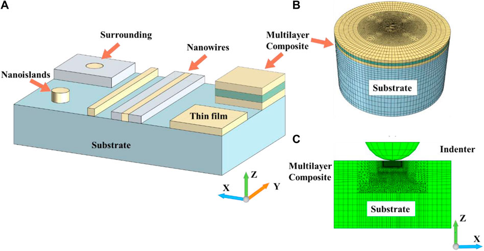
FIGURE 1. (A) Schematic illustrating the indentation of piezoelectric composites: nanoislands, nanowires, thin film and multilayer composites with surrounding and substrate (piezoelectric materials is poled along the Z direction), (B) the illustration of the finite element model for three layers piezoelectric composites and (C) the cross-sectional image of the finite element model for characterizing the indentation response of three layers piezoelectric composites (indentation direction is along the Z direction).
For multi-layered composites, three types of composites, i.e., double, triple, and quadruple layered composites are considered. As shown in Figure 2, there are two combinations for the double-layered structures, six combinations for the triple layered-structures, and fourteen combinations for the quadruple layered-structures. In all cases, the thickness of each layer is fixed at 1000 nm. For all the layered composites, a 20 μm thick silicon wafer is used as the substrate and a very thin layer of platinum is also included as an electrode/current collector.
The effect of lateral constraints introduced by surrounding materials on the indentation response of nano-island and nano-wire structures, is captured by models that include metallic and piezoelectric surrounding materials. Four types of substrate materials are considered, i.e., compliant elastic material (Si), stiff elastic material (SiC), compliant elastic-plastic material (Al 6061-T4), and stiff elastic-plastic material (Steel—A36) (Table 1).
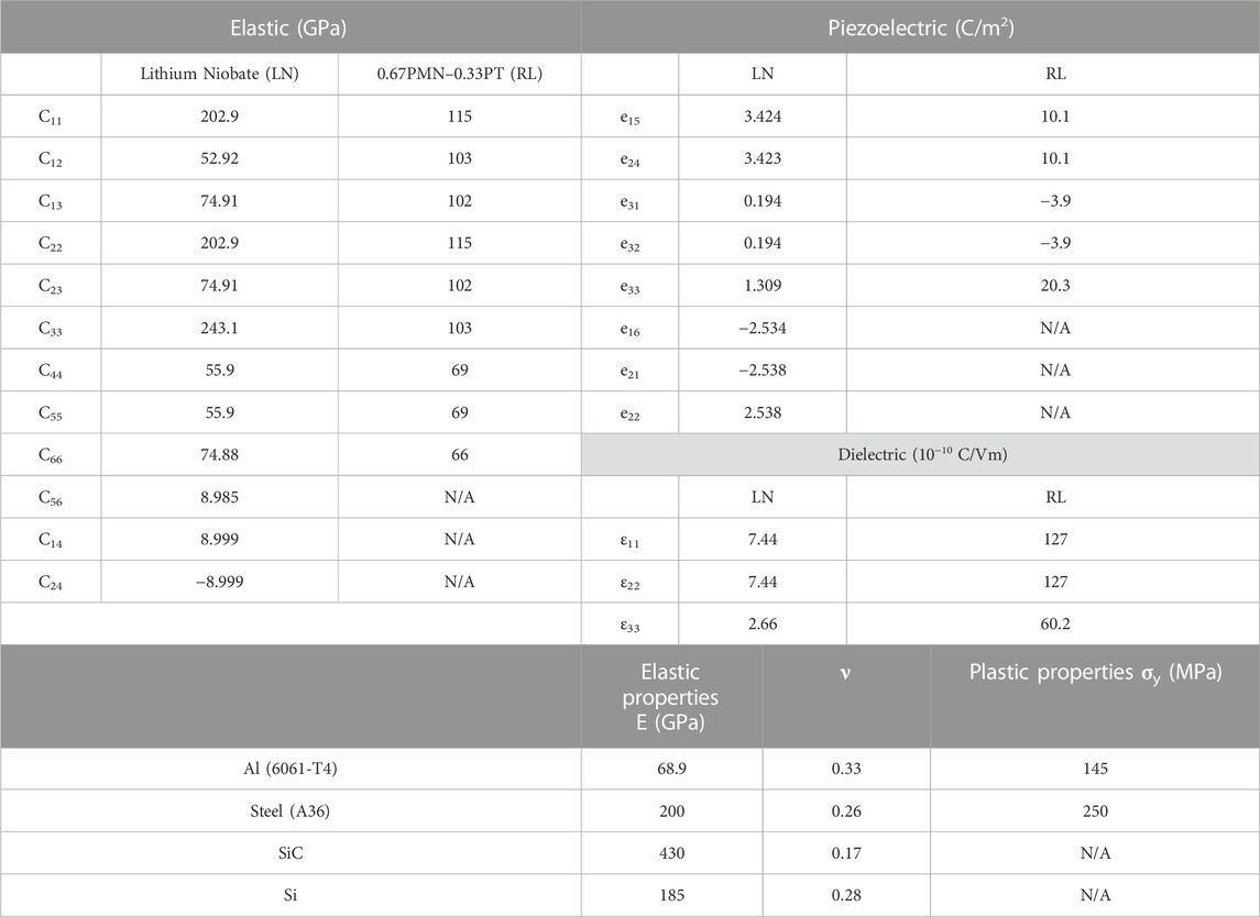
TABLE 1. Materials properties of piezoelectric materials and the substrate materials used in the current study.
The minimum length-scales considered in the present study are 200 nm for the piezoelectric layer, 1000 nm for the nano-wire height and width and 1000 nm for the radius of the nano-island structures. These length-scales are large enough that the loss of piezoelectricity observed at smaller length-scales (e.g., below 10 nm in BaTiO3) need not be considered (Buscaglia and Randall, 2020). A commercially available software package ABAQUS is used for developing the model and conducting simulations. Three-dimensional finite element models are constructed with over 400,000 three-dimensional elements, such as 8-node linear piezoelectric brick (C3D8E) elements and 8-node linear brick reduced integration (C3D8R) elements as illustrated in Figures 1B, C. The boundary conditions for the materials and the indenters (such as electrically conducting and insulting) were set up as those in our previous studies (Cheng and Venkatesh, 2012; Cheng and Venkatesh, 2013). The models are designed such that at least 50 elements are in contact with the indenter at maximum indentation depth in order to accurately obtain the electric charge generated during the indentation process. As described in Section 4, indentation simulations are conducted with several spherical and conical indenters. The indentation force-depth and charge-depth relationships are obtained to understand the indentation behavior of piezoelectric small-volume structures and layered composites. For the indentation of layered composites, the maximum indentation depth is limited to less than 15% of the first layer thickness along the loading direction so that the effect of potential cracking need not be considered in this study.
Some prior studies based on piezo force microscopy have indicated that high, localized electrical fields may be generated under certain loading conditions, which may cause piezoelectric domain switching (Grigoriev et al., 2006) and domain wall movements (Schellekens et al., 2012; McGilly et al., 2015) or ferroelectric and ferroelastic switching (Hwang et al., 1995), that result in a non-linear electromechanical coupling of the piezoelectric materials. However, in previous indentation studies with spherical indenters, it has been demonstrated that the electric fields generated near the indented regions are not very high and good agreement between simulation results and experiments (Nili et al., 2013; Cheng et al., 2014) is obtained without considering such effects. Hence, in the present study, the constitutive behavior of piezoelectric materials under indentation loading is considered to be linear and any non-linearity associated with domain wall movements is ignored.
Three dimensional finite element models of indentation of piezoelectric small-volume structures such as nano-islands and nano-wires (in the form of hemispherical domes and cylinders) with sharp indenters, were validated with experimental results in an earlier study (Cheng et al., 2014), as shown in Figure 3. The mechanical and electrical indentation responses observed in the spherical indentation of three types of piezoelectric small-volume structures, i.e., nano-islands, nano-wires and thin films were also discussed in a recent study (Cheng et al., 2022). It was found that, in general, the indentation response of thin film piezoelectric structures was much stiffer than that of the piezoelectric nano-islands and nano-wires which resulted in more charge accumulation during the indentation of thin film piezoelectric structures. However, the differences in the charge accumulations were reduced as the characteristic feature size (i.e., the height of the nano-island or the thickness of the thin film) was increased. The larger-sized nano-island and nano-wire structures were found to be stiffer than their smaller-sized counterparts, while, the opposite trend was observed in the case of thin films. The observed trend in the indentation response of thin films was attributed to the influence of the substrate material which was noted to become less pronounced when the thickness of thin film was increased.
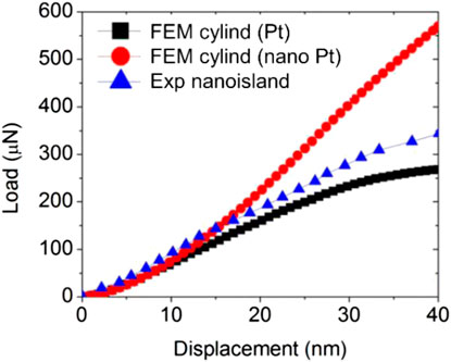
FIGURE 3. The load-displacement curves for the indentation of PSZT nanoislands with different Pt substrates (FEM denotes finite element modeling, Exp denotes experimental obtained load-displacement curve, Pt denotes the soft Pt substrate is utilized in the FEM, and nano Pt denotes stiff Pt substrate is utilized in the FEM). (Cheng et al., 2014).
In the present study, the influence of surrounding materials on the indentation response of nano-island structures (cylindrically-shaped with a radius of 1000 nm) and nano-wires (height/width = 1, height = 1000 nm) of relaxor ferroelectrics, are investigated, as shown in Figure 1. Two metallic materials, Al and Fe, with elastic-plastic properties and two piezoelectric materials, 0.67PMN-0.33PT and lithium niobate, are considered as surrounding materials. Indentations with six kinds of indenters: three spherical indenters (1.5 µm radius, 2 µm radius and 10 µm radius) and three conical indenters with (55° apex angle, 70° apex angle and 83° apex angle) are modeled. The corresponding indentation force-depth and charge-depth relationships obtained in this study are presented in Figures 4, 5, 6.
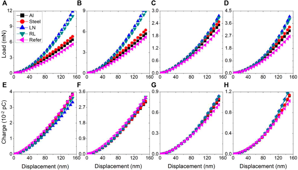
FIGURE 4. The force-depth and charge-depth responses obtained from R = 2 µm spherical indenter (A, E), R = 1.5 µm spherical indenter (B, F), theta = 55° conical indenter (C, G) and theta = 70° conical indenter (D, H) on relaxor piezoelectric nanoislands (hemispherical shaped) with a silicon substrate (Al denotes aluminum acting as the surrounding material, Steel denotes steel acting as the surrounding material, LN denotes lithium niobate acting as surrounding materials, RL denotes relaxor ferroelectric materials acting as the surrounding materials, and Refer denotes indentation on relaxor nanostructures without any surrounding materials).
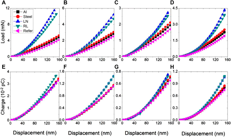
FIGURE 5. The force-depth and charge-depth responses obtained from R = 2 µm spherical indenter (A, E), R = 1.5 µm spherical indenter (B, F), theta = 55° conical indenter (C, G) and theta = 70° conical indenter (D, H) on relaxor piezoelectric nanowires with a silicon substrate (Al denotes aluminum acting as the surrounding material, Steel denotes steel acting as the surrounding material, LN denotes lithium niobate acting as surrounding materials, RL denotes relaxor ferroelectric materials acting as the surrounding materials, and Refer denotes indentation on relaxor nanostructures without any surrounding materials).
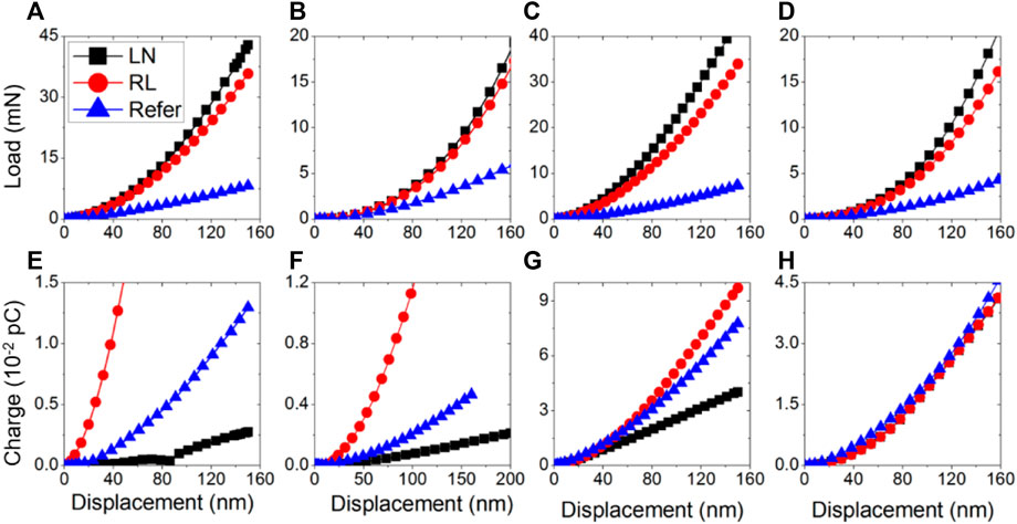
FIGURE 6. The force-depth and charge-depth responses obtained from R = 10 µm spherical indenter on relaxor nanoislands (A, E), theta = 83° conical indenter on relaxor nanoislands (B, F), R = 10 µm spherical indenter on relaxor nanowire (C, G), theta = 83° conical indenter on relaxor nanowire (D, H), with a silicon substrate (LN denotes lithium niobate acting as surrounding materials, RL denotes relaxor ferroelectric materials acting as the surrounding materials, and Refer denotes indentation on relaxor nanostructures without any surrounding materials).
For piezoelectric nano-islands and nano-wires, the mechanical indentation response of nanostructures with surrounding materials was stiffer and generated more electric charges than nanostructures without the surrounding materials, when the indentations were performed with spherical indenters (R = 1.5 µm and R = 2 µm) and conical indenters (55° and 70°). It is expected that the lateral constrain introduced by the surrounding materials will inhibit the deformation of nanostructures in the direction of loading and increase the contact between indenters and the nanostructures. However, from the force-depth and charge-depth relationships, it is noted that this effect is not very significant as the indentation depth is not greater than 15% of the thickness of the structures.
The effect of the surrounding materials is strongly dependent on their elastic property as well as their electrical conductivity. Amongst the metallic materials considered as surrounding materials, steel (with a higher elastic modulus) contributes to a higher effect as compared to that produced by aluminum. Similarly, amongst ceramic materials considered as surrounding materials, the effect of lithium niobate (with a higher C33) is also much stronger than that of 0.67PMN-0.33PT.
The effect of the surrounding material is influenced by its electric conductivity, esp., for metallic materials. The elastic modulus of aluminum is higher than that of 0.67PMN-0.33PT and the modulus of steel is higher than that of lithium niobate. However, the mechanical indentation stiffness of the piezo structures, with metals as the surrounding materials, is less, than in the case of the piezo structures with ceramic surrounding material, as the metallic materials create a new boundary condition to the nanostructures and generate zero-potential regions on the surface of the nanostructures. This electrical boundary condition greatly changes the internal electric field generated by the piezoelectric coupling and weakens the effective piezoelectric effects.
When the contacting regions, during indentation, extend beyond the nanostructures, (as in the case of a spherical indenter (R = 10 µm) and a conical indenter (θ = 83°)), it is found that nanostructures with stiffer surrounding materials (i.e., LN) are mechanical stiffer than those with softer surrounding materials (i.e., RL), for both indenters. As demonstrated in a previous study (Cheng and Venkatesh, 2012; Cheng and Venkatesh, 2013), the mechanical indentation stiffness shows a strong dependence on the normal elastic component (C33). Thus, the mechanical indentation stiffness of the indented system RL (with LN as the surrounding material) is higher than that of the indented system RL (with RL as the surrounding material, which is just a uniform RL thin film). The piezoelectric indentation stiffness of the indented (RL) nano-structures is also influenced by the nature of the surrounding materials. The effect of lithium niobate as a surrounding material is to reduce the piezoelectric indentation stiffness to a level that is lower than that observed in the relaxor nano-structures that do not have any surrounding materials.
Furthermore, it is also observed that the geometry of the indenter could influence the electric charges generated during the indentation process. The spherical indenter generates the highest electric charges at the fringes of the contacting areas, while the conical indenter generates the most electric charges at the center of the contacting area. This may be attributed to the higher levels of stress concentrations obtained close to the tip of the indenter in the case of a sharp conical indenter. When the conducting indenters contact the nanoislands (or nanowires) and the surrounding materials, most of the electric charges are collected from the surrounding materials, in the case of the spherical indenter, unlike in the case of a conical indenter. Hence, the variation in the observed piezoelectric response is much more pronounced in case of indentations with a spherical indenter than with that of a conical indenter.
A comprehensive analysis of the nanoindentation response of multilayered composites was conducted by modeling the indentation of 22 types on multilayered composites, (each comprising of two piezoelectric materials), on silicon substrates, with a spherical indenter (with radius R = 10 µm). In all cases, the depth of indentation was limited to no more than 15% of the first layer. Three kinds of multilayered composites—double-layered (two combinations), triple-layered (six combinations), and quadruple-layered (fourteen combinations) structures, all of which had the same layer thickness of 1000 nm were designed. Two anisotropic piezoelectric materials-relaxor ferroelectric (RL) (0.67PMN-0.33PT) with a high piezoelectric coefficient and lithium niobate (LN) with a high elastic stiffness, were selected (and respectively, designated as material A and material B). Indentation simulations were performed with electrically conducting and insulating indenters.
From the force-depth indentation response observed in the double-layered and triple-layered structures (shown in Figures 7A, C and Figures 8A, C), it is evident that bulk lithium niobate (named as LN standard in Figure 7A) always provided the most stiff nanoindentation response. This observation can be related to the fact that lithium niobate has the highest value for the elastic stiffness constant - C33, which has been demonstrated to have the largest influence on the mechanical indentation stiffness. Meanwhile, bulk relaxor ferroelectric material (named as RL standard in Figure 7A), with the least value for the elastic stiffness constant C33, exhibits the most compliant indentation response amongst all the combinations considered. This observation is consistent with (experimental and finite element) results reported earlier on the indentation response of metal-metal or metal-ceramic multi-layered systems (where the thickness of each layer is greater than 100 nm such that the indentation size-effect is avoided), which indicated that the effective mechanical indentation response of multilayered composites was in-between that of the soft and stiff layers (Liu et al., 1996; Ha et al., 2001; Cleymand et al., 2005).
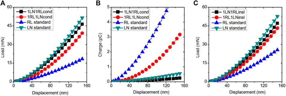
FIGURE 7. The force-depth and charge-depth response obtained from spherical indentations (10 µm) on piezoelectric with double-layers piezoelectric structures: (A) force-depth curves under conducting indenter (B) charge-depth curves under conducting indenter, and (C) force-depth curves under insulating indenter (1RL1LN denotes the first layer is relaxor ferroelectric materials and the second layer is lithium niobate, RL standard denotes nanoindentation response on bulk relaxor ferroelectric materials).

FIGURE 8. The force-depth and charge-depth response obtained from spherical indentations (10 µm) on three layers piezoelectric structures: 1RL1LN1RL denotes the first layer is relaxor ferroelectric material, the second layer is lithium niobate and the third layer is relaxor ferroelectric; 1RL2LN standard denotes first layer is relaxor ferroelectric material and next 2 layers are lithium niobate. (A) force-depth curves under conducting indenter (B) charge-depth curves under conducting indenter, and (C) force-depth curves under the insulating indenter.
From the charge-depth indentation response observed in the double-layered and triple-layered structures (as shown in Figure 7B and Figure 8B), it is evident that the bulk relaxor ferroelectric material always provided the highest piezoelectric nanoindentation stiffness. This observation can be related to the fact that the relaxor ferroelectric has the highest piezoelectric constant, e33, which has been shown to have the most dominant effect on the effective piezoelectric indentation stiffness. However, bulk lithium niobate does not provide the least piezoelectric indentation stiffness at the same indentation depth. The double-layered structure 1LN1RL (which denotes the first layer to be lithium niobate and the second layer to be relaxor ferroelectric) and the triple-layered structure 1LN2RL, exhibit the least piezoelectric indentation stiffness amongst the double-layered and triple-layered structures, respectively. This observation may be related to the negative values of the piezoelectric constants e31 and e32, exhibited by the relaxor ferroelectric layers.
The indentation response of all the 14 combinations of quadruple structures was analyzed (and summarized in Table 2). The principal result from this analysis is that the multi-layered structures considered in this study exhibit effective piezoelectric and mechanical indentation stiffnesses that are bounded by the corresponding characteristics of the bulk material counterparts. The upper bounds in the piezoelectric and mechanical indentation stiffness correspond to that of the bulk relaxor ferroelectric material (which has the maximum piezoelectric indentation constant, e33) and bulk lithium niobate (which has the maximum mechanical indentation constant, C33). The lowest mechanical indentation stiffness is observed in the 3R1L system while the lowest piezoelectric indentation stiffness is observed in the 1L3R system.
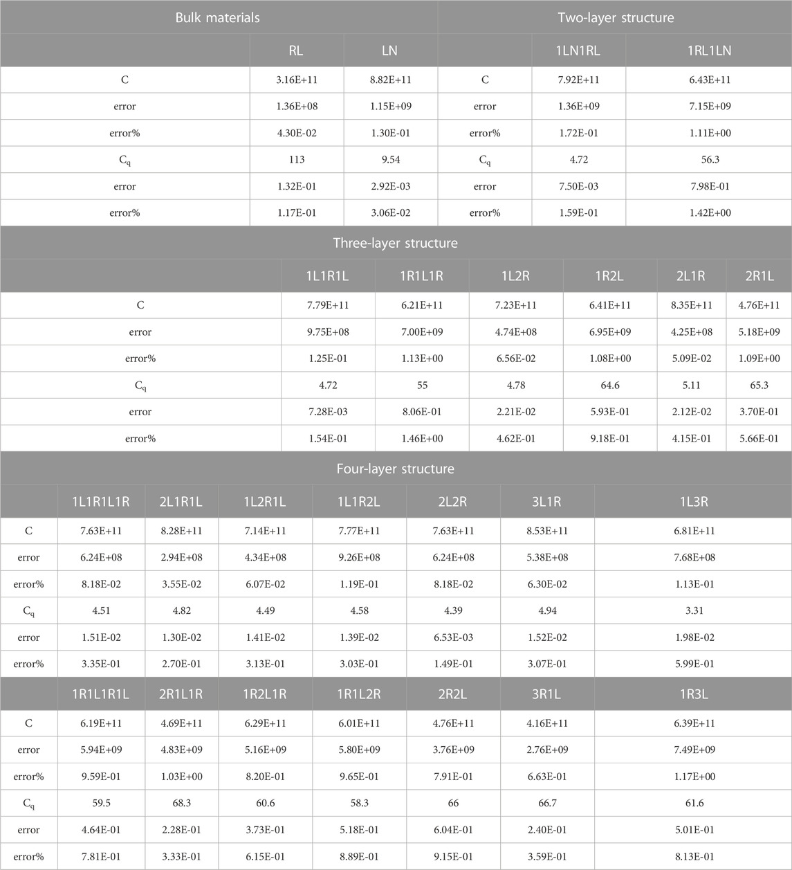
TABLE 2. The mechanical and electrical indentation stiffness (i.e., C and Cq, respectively) obtained from the finite element modeling of indentation of multi-layered piezoelectric composites with a spherical indenter. (The mechanical and electric indentation response of multilayers are, respectively, captured by power laws P = Ch1.5 (the unit of C = µN/(nm)−1.5) and Q = Cqh1.5 (the unit of Cq = 10−2 pC/(nm) −1.5). Standard denotes the indentation on bulk piezoelectric materials, L or LN denotes lithium niobate, and R or RL denotes relaxor ferroelectric materials 0.67PMN-0.33PT.).
In order to assess the effect of the stiffness of the substrate material on the indentation response of multi-layered piezoelectric composites, simulations were performed on structures with a substrate (SiC) that is stiffer than Si. SiC has an elastic modulus of 430 GPa (Wolfenden et al., 1999). The force-depth and charge-depth indentation relationships observed in thin films with different thickness are shown in Figure 9. It is found that the substrate determines the indentation response from the onset of indentation, with no significant discontinuities or inflections in the loading curves. The silicon carbide substrate renders the thin films stiffer and contributes to greater charges being generated during the indentation process, at the same indentation depth, than with the more compliant silicon substrate.
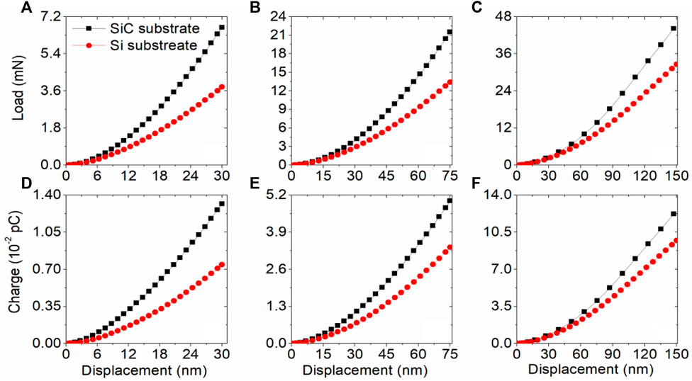
FIGURE 9. The force-depth and charge-depth response obtained from conducting spherical indentations on piezoelectric thin films with silicon and silicon carbide substrate: (A) force-depth of 200 nm thin film (D) charge-depth of 200 nm thin film (B) force-depth of 500 nm thin film (E) charge-depth of 500 nm thin film (C) force-depth of 1000 nm thin film (F) charge-depth of 1000 nm thin film.
In order to assess the effect of plastic deformation in the substrate material, on the indentation response of piezoelectric multi-layered composites, two metallic materials—aluminum and steel, are considered. The elastic modulus and yield strength of steel is substantially higher than that of aluminum (Table 1). For a comparative study, two cases, purely elastic deformation (see Al and Fe in Figure 10) and elastic-perfectly plastic deformation (see Al E + P and Fe E + P in Figure 10) in the substrate material were considered. In the previous study, the influence of the elastic-plastic substrate on the nanoindentation response of transversely isotropic piezoelectric materials and piezoelectric nanoislands was investigated (Nili et al., 2013; Cheng et al., 2014). The stiffer substrate contributes to higher mechanical and electrical indentation stiffness. This observation could be explained by the fact that a softer piezoelectric film on a stiff substrate (steel) renders the indentation pile-up effect to be more significant, leading to a larger contact area than in the case of the indentation of a stiffer piezoelectric film on a softer substrate material (Al).
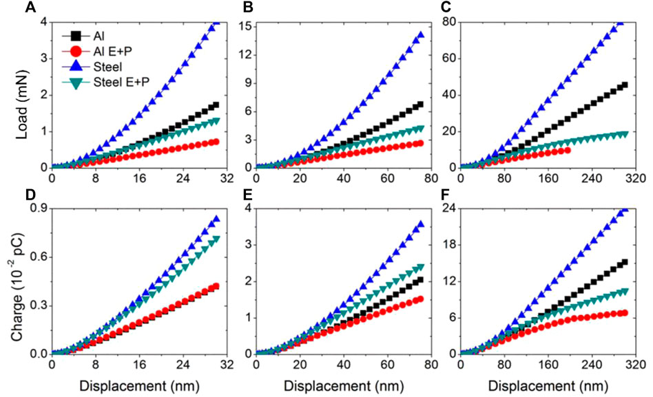
FIGURE 10. The force-depth and charge-depth response obtained from conducting spherical indentations (10 µm) on piezoelectric thin films with different substrate considering elastic and plastic properties: Al denotes substrate with only elastic properties and Al E + P denotes substrate with both elastic and plastic properties: (A) force-depth of 200 nm thin film (D) charge-depth of 200 nm thin film (B) force-depth of 500 nm thin film (E) charge-depth of 500 nm thin film (C) force-depth of 1000 nm thin film (F) charge-depth of 1000 nm thin film.
When the substrate material is allowed to deform plastically, it is observed that the plastic deformation starts to affect the mechanical indentation response of piezoelectric materials when the indentation depths reach to about 10% of film thickness, which has also been observed in a previous study on the indentation of PSZT materials (Cheng et al., 2014).
The plastic deformation of the aluminum substrate does not influence the electric indentation response of the piezoelectric film when the film thickness is 200 nm, and the indentation depth is 30 nm. When the indentation depth reaches 15% of the 200 nm film thickness, a 20% difference in the amount of electric charge collected from the thin film on the Al substrate which deforms elastically and from the thin film on the Al substrate which deforms plastically as well. The 20% difference in the electric charge generation was found at 11% indentation depth for the 500 nm thin films and at 10% indentation depth for 1000 nm thin films.
The steel substrate does not influence the piezoelectric indentation response significantly when the thickness of the relaxor ferroelectric film is 200 nm and the indentation depth is 15% of the film thickness (i.e., 30 nm). A significant difference (i.e., over 20% in electrical charge generation), during the indentation of the thin films on the steel substrates (that deform elastically and plastically) is found after indenting up to 8% of the film thickness in the case of the films with 500 nm and 1000 nm thicknesses.
Hence, the present study is focused on obtaining a comprehensive understanding of the factors influencing the force-depth mechanical indentation response and the charge-depth electrical indentation response of micro- and nano-piezoelectric composites considering the substrate and surrounding materials. From the analysis of a large number of three-dimensional finite element simulations of the indentation response of a wide variety of small-volume piezoelectric composites, the following principal conclusions are obtained:
(1) The elastic properties of the underlying substrate materials have a profound influence on the indentation response of the piezoelectric composites even though the substrate does not get indented. A substrate material that is elastically stiffer than the piezoelectric material affects the indentation response of the piezoelectric composites from the onset of indentation. The stiffer substrate enhances the mechanical indentation stiffness and the electric indentation stiffness, resulting in the accumulation of more electric charges during the indentation process as compared to a piezoelectric structure that is supported by a substrate that is elastically more compliant.
(2) The plastic properties of the substrate material also have an important influence on the effective indentation response of the piezoelectric composites. The effect of plastic deformation is similar to that created by an elastically compliant substrate, resulting in reduction of the mechanical indentation stiffness and a reduction in the electrical charges generated during the indentation process, as compared to the case where the substrate does not undergo plastic deformation. For the piezoelectric composites considered, the softening effects due to substrate plasticity are apparent when the indentation depths reach about 8%–15% of the thickness of the piezoelectric structure in the direction of indentation.
(3) From a comprehensive study of the indentation response of 22 combinations of multilayered piezoelectric composites that are obtained from various combinations of two piezoelectric materials, it is observed that, in general, the indentation behavior is largely influenced by the properties of the first layer that is indented and the adjacent layers that are present close to the indented layer. For the multi-layered structures which are considered in the present study, the effective piezoelectric and mechanical indentation stiffnesses are bounded by the corresponding characteristics of the bulk material counterparts. The upper bounds in the piezoelectric and mechanical indentation stiffness correspond to that of the bulk material (which has the maximum piezoelectric indentation constant, e33) and the bulk material (which has the maximum mechanical indentation constant, C33).
(4) In addition to the substrate materials that function as supporting entities for the piezoelectric composites, the natures of the surrounding materials also play a crucial role in determining the indentation response of piezoelectric composites. Electrically conducting surrounding materials produce a softening effect while insulating materials enhance the electrical indentation stiffness resulting in more charges being accumulated during the indentation process.
Overall, the results obtained in the present study are expected to provide useful insights on the complex interplay between the elastic, piezoelectric and dielectric properties of the piezoelectric composites, their size and shape and the (elastic, plastic and conducting) nature of the substrate and surrounding materials, on the indentation response of piezoelectric micro- and nano-composites. The stiff surrounding materials in piezoelectric small-volume structures would enhance charge generation in piezoelectric devices made from such composites when they are used in energy harvesting and sensor application. Layered or laminated piezoelectric structures are more likely to be used in devices where mechanical stiffness and robustness are required. These insights would be helpful for the design, fabrication and testing of novel piezoelectric small volume structures for many smart device applications.
The original contributions presented in the study are included in the article/Supplementary Material, further inquiries can be directed to the corresponding author.
GC: Conceptualization, draft, Writing–Original, Investigation, Writing–Review and Editing, Supervision, Funding acquisition; ZW: Writing–Original, draft, Investigation, Visualization; TV: Conceptualization, Writing–Review and Editing, Investigation, Supervision, Funding acquisition. All authors contributed to the article and approved the submitted version.
GC and ZW acknowledges project funding, the Fundamental Research Funds for the Central Universities (buctrc201827) and National Natural Science Foundation of China (51905026). TV acknowledges partial support from the Office of Naval Research for this study.
The authors declare that the research was conducted in the absence of any commercial or financial relationships that could be construed as a potential conflict of interest.
All claims expressed in this article are solely those of the authors and do not necessarily represent those of their affiliated organizations, or those of the publisher, the editors and the reviewers. Any product that may be evaluated in this article, or claim that may be made by its manufacturer, is not guaranteed or endorsed by the publisher.
Bahr, D. F., Robach, J. S., Wright, J. S., Francis, L., and Gerberich, W. (1999). Mechanical deformation of PZT thin films for MEMS applications. Mater. Sci. Eng. A 259 (1), 126–131. doi:10.1016/S0921-5093(98)00868-5
Ballas, R. (2007). Piezoelectric multilayer beam bending actuators static and dynamic behavior and aspects of sensor integration. Heidelberg, Baden-Württemberg, Germany: Physica-Verlag.
Baniasadi, M., Xu, Z., Cai, J., Daryadel, S., Quevedo-Lopez, M., Naraghi, M., et al. (2017). Correlation of annealing temperature, morphology, and electro-mechanical properties of electrospun piezoelectric nanofibers. Polymer 127, 192–202. doi:10.1016/j.polymer.2017.08.053
Blonsky, M. N., Zhuang, H. L., Singh, A. K., and Hennig, R. G. (2015). Ab initio prediction of piezoelectricity in two-dimensional materials. ACS Nano 9 (10), 9885–9891. doi:10.1021/acsnano.5b03394
Buscaglia, V., and Randall, C. A. (2020). Size and scaling effects in barium titanate. An overview. J. Eur. Ceram. Soc. 40 (11), 3744–3758. doi:10.1016/j.jeurceramsoc.2020.01.021
Cady, W. G. (1964). Piezoelectricity: An introduction to the theory and applications of electromechanical phenomena in crystals. Mineola, New York, United States: Dover Publications.
Chamankar, N., Khajavi, R., Yousefi, A. A., Rashidi, A., and Golestanifard, F. (2020). A flexible piezoelectric pressure sensor based on PVDF nanocomposite fibers doped with PZT particles for energy harvesting applications. Ceram. Int. 46 (12), 19669–19681. doi:10.1016/j.ceramint.2020.03.210
Cheng, G., Choi, K. S., Hu, X., and Sun, X. (2016). Determining individual phase properties in a multi-phase Q&P steel using multi-scale indentation tests. Mater. Sci. Eng. A 652, 384–395. doi:10.1016/j.msea.2015.11.072
Cheng, G., Lu, Y., and Venkatesh, T. A. (2022). Indentation of piezoelectric micro- and nanostructures. Int. J. Mod. Phys. B 36, 09N11. doi:10.1142/S0217979222400355
Cheng, G., Sriram, S., Bhaskaran, M., and Venkatesh, T. A. (2014). Nanoindentation response of piezoelectric nano-islands. Appl. Phys. Lett. 105 (12). doi:10.1063/1.4896128
Cheng, G., and Venkatesh, T. A. (2013). Dominant factors influencing the nanoindentation response of piezoelectric materials: A case study in relaxor ferroelectrics. Philos. Mag. Lett. 93 (2), 116–128. doi:10.1080/09500839.2012.752881
Cheng, G., and Venkatesh, T. A. (2012). Nanoindentation response of anisotropic piezoelectric materials. Philos. Mag. Lett. 92 (6), 278–287. doi:10.1080/09500839.2012.669054
Chung, S. Y., Kim, S., Lee, J. H., Kim, K., and Kang, C., (2012). All-solution-processed flexible thin film piezoelectric nanogenerator. Adv. Mater. 24 (45), 6022–6027. doi:10.1002/adma.201202708
Cleymand, F., Ferry, O., Kouitat, R., Billard, A., and von Stebut, J. (2005). Influence of indentation depth on the determination of the apparent young's modulus of bi-layer material: experiments and numerical simulation. Surf. Coatings Technol. 200 (1-4), 890–893. doi:10.1016/j.surfcoat.2005.02.086
Cui, H. C., Hensleigh, R., Yao, D. S., Maurya, D., Kumar, P., Kang, M. G., et al. (2019). Three-dimensional printing of piezoelectric materials with designed anisotropy and directional response. Nat. Mater. 18 (3), 234–241. doi:10.1038/s41563-018-0268-1
Duerloo, K.-A., Ong, M., and Reed, E. (2012). Intrinsic piezoelectricity in two-dimensional materials. J. Phys. Chem. Lett. 3, 2871–2876. doi:10.1021/jz3012436
Gall, K., Juntunen, K., Maier, H. J., Sehitoglu, H., and Chumlyakov, Y. (2001). Instrumented micro-indentation of NiTi shape-memory alloys. Acta Mater. 49 (16), 3205–3217. doi:10.1016/S1359-6454(01)00223-3
Gao, P. X., Song, J., Liu, J., and Wang, Z. (2007). Nanowire piezoelectric nanogenerators on plastic substrates as flexible power sources for nanodevices. Adv. Mater. 19 (1), 67–72. doi:10.1002/adma.200601162
Gino, M. E., Selleri, G., Cocchi, D., Brugo, T. M., Testoni, N., De Marchi, L., et al. (2022). On the design of a piezoelectric self-sensing smart composite laminate. Mater. Des. 219, 110783. doi:10.1016/j.matdes.2022.110783
Grigoriev, A., Do, D.-H., Kim, D. M., Eom, C. B., Adams, B., Dufresne, E. M., et al. (2006). Nanosecond domain wall dynamics in ferroelectric Pb(Zr,Ti)O-3 thin films. Phys. Rev. Lett. 96 (18), 187601. doi:10.1103/PhysRevLett.96.187601
Ha, H. C., Chan, H. M., and Nied, H. F. (2001). Hertzian contact behavior of alumina-based trilayer composites: experimental observation and fem analysis. Acta Mater. 49 (13), 2453–2461. doi:10.1016/S1359-6454(01)00151-3
Hadraba, H., Chlup, Z., Drdlík, D., and Šiška, F. (2020). Characterisation of mechanical and fracture behaviour of Al2O3/ZrO2/BaTiO3 laminate by indentation. J. Eur. Ceram. Soc. 40 (14), 4799–4807. doi:10.1016/j.jeurceramsoc.2020.04.024
Hinchet, R., Khan, U., Falconi, C., and Kim, S. W. (2018). Piezoelectric properties in two-dimensional materials: simulations and experiments. Mater. Today 21 (6), 611–630. doi:10.1016/j.mattod.2018.01.031
Hinterdorfer, P., and Dufrene, Y. F. (2006). Detection and localization of single molecular recognition events using atomic force microscopy. Nat. Methods 3 (5), 347–355. doi:10.1038/NMETH871
Hwang, S. C., Lynch, C. S., and McMeeking, R. M. (1995). Ferroelectric/ferroelastic interactions and a polarization switching model. Acta Metallurgica Materialia 43 (5), 2073–2084. doi:10.1016/0956-7151(94)00379-V
Ico, G., Showalter, A., Bosze, W., Gott, S. C., Kim, B. S., Rao, M. P., et al. (2016). Size-dependent piezoelectric and mechanical properties of electrospun P(VDF-TrFE) nanofibers for enhanced energy harvesting. J. Mater. Chem. A 4 (6), 2293–2304. doi:10.1039/C5TA10423H
Jaffe, B., and Jaffe, H. (1971). Piezoelectric ceramics. Cambridge, Massachusetts, United States: Academic Press.
Kamble, S. N., Kubair, D. V., and Ramamurty, U. (2009). Indentation strength of a piezoelectric ceramic: experiments and simulations. J. Mater. Res. 24 (3), 926–935. doi:10.1557/JMR.2009.0115
Karaki, T., Yan, K., Miyamoto, T., and Adachi, M. (2007). Lead-free piezoelectric ceramics with large dielectric and piezoelectric constants manufactured from BaTiO3 nano-powder. Jpn. J. Appl. Phys. 46 (4-7), L97–L98. doi:10.1143/JJAP.46.L97
Kim, G., Seo, M. K., Choi, N., Kim, Y. I., and Kim, K. B. (2019). Comparison of PZT, PZT based 1-3 composite and PMN-PT acoustic emission sensors for glass fiber reinforced plastics. Int. J. Precis. Eng. Manuf. 20 (6), 1007–1015. doi:10.1007/s12541-019-00055-7
Lan, H., and Venkatesh, T. A. (2014). On the relationships between hardness and the elastic and plastic properties of isotropic power-law hardening materials. Philos. Mag. 94 (1), 35–55. doi:10.1080/14786435.2013.839889
Lee, D.-H., Seok, M.-Y., Zhao, Y., Choi, I. C., He, J., Lu, Z., et al. (2016). Spherical nanoindentation creep behavior of nanocrystalline and coarse-grained CoCrFeMnNi high-entropy alloys. Acta Mater. 109, 314–322. doi:10.1016/j.actamat.2016.02.049
Lefki, K., and Dormans, G. J. M. (1994). Measurement of piezoelectric coefficients of ferroelectric thin films. J. Appl. Phys. 76 (3), 1764–1767. doi:10.1063/1.357693
Liu, H., Lawn, B. R., and Hsu, S. M. (1996). Hertzian contact response of tailored silicon nitride multilayers. J. Am. Ceram. Soc. 79 (4), 1009–1014. doi:10.1111/j.1151-2916.1996.tb08540.x
McGilly, L. J., Yudin, P., Feigl, L., Tagantsev, A. K., and Setter, N. (2015). Controlling domain wall motion in ferroelectric thin films. Nat. Nanotechnol. 10 (2), 145–150. doi:10.1038/NNANO.2014.320
Melkumyan, S. A., and Ulitko, A. F. (1987). Axisymmetric contact problem of electroelasticity for a half-space. Sov. Appl. Mech. 23 (9), 836–843. doi:10.1007/BF00887786
Newnham, R. E., Skinner, D. P., and Cross, L. E. (1978). Connectivity and piezoelectric-pyroelectric composites. Mater. Res. Bull. 13 (5), 525–536. doi:10.1016/0025-5408(78)90161-7
Nili, H., Cheng, G., Venkatesh, T. A., Sriram, S., and Bhaskaran, M. (2013). Correlation between nanomechanical and piezoelectric properties of thin films: an experimental and finite element study. Mater. Lett. 90, 148–151. doi:10.1016/j.matlet.2012.09.036
Qi, Y., Kim, J., Nguyen, T. D., Lisko, B., Purohit, P. K., and McAlpine, M. C. (2011). Enhanced piezoelectricity and stretchability in energy harvesting devices fabricated from buckled PZT ribbons. Nano Lett. 11 (3), 1331–1336. doi:10.1021/nl104412b
Qin, Y., Wang, X., and Wang, Z. L. (2009). Erratum: microfibre–nanowire hybrid structure for energy scavenging. Nature 457 (7227), 340. doi:10.1038/nature07628
Ramadan, K., Sameoto, D., and Evoy, S. (2014). A review of piezoelectric polymers as functional materials for electromechanical transducers. Smart Mater. Struct. 23, 033001. doi:10.1088/0964-1726/23/3/033001
Ramamurty, U., Sridhar, S., Giannakopoulos, A. E., and Suresh, S. (1999). An experimental study of spherical indentation on piezoelectric materials. Acta Mater. 47 (8), 2417–2430. doi:10.1016/S1359-6454(99)00095-6
Saigal, A., Giannakopoulos, A. E., Pettermann, H. E., and Suresh, S. (1999). Electrical response during indentation of a 1-3 piezoelectric ceramic-polymer composite. J. Appl. Phys. 86 (1), 603–606. doi:10.1063/1.370773
Schellekens, A. J., van den Brink, A., Franken, J. H., Swagten, H., and Koopmans, B. (2012). Electric-field control of domain wall motion in perpendicularly magnetized materials. Nat. Commun. 3, 847. doi:10.1038/ncomms1848
Shindo, Y., Yoshida, M., Narita, F., and Horiguchi, K. (2004). Electroelastic field concentrations ahead of electrodes in multilayer piezoelectric actuators: experiment and finite element simulation. J. Mech. Phys. Solids 52 (5), 1109–1124. doi:10.1016/j.jmps.2003.09.017
Song, H. C., Kim, H. C., Kang, C. Y., Yoon, S. J., and Jeong, D. Y. (2009). Multilayer piezoelectric energy scavenger for large current generation. J. Electroceramics 23 (2-4), 301–304. doi:10.1007/s10832-008-9439-9
Sriram, S., Bhaskaran, M., Ahluwalia, R., Nguyen, T. G., Ng, N., Srolovitz, D. J., et al. (2011). Surface morphology induced localized electric field and piezoresponse enhancement in nanostructured thin films. ACS Nano 5 (2), 1067–1072. doi:10.1021/nn103561u
Tian, M., and Venkatesh, T. A. (2013). Indentation of shape memory polymers: characterization of thermomechanical and shape recovery properties. Polymer 54 (4), 1405–1414. doi:10.1016/j.polymer.2012.12.075
Tichý, J., Kittinger, E., and Privratska, J. (2010). Fundamentals of piezoelectric sensorics: Mechanical, dielectric, and thermodynamical properties of piezoelectric materials. Berlin, Germany: Springer Science & Business Media.
Venkatesh, T. A., Van Vliet, K. J., and Giannakopoulos, A. E., (2000). Determination of elasto-plastic properties by instrumented sharp indentation: guidelines for property extraction. Scr. Mater. 42 (9), 833–839. doi:10.1016/S1359-6462(00)00311-0
Wang, Y., Yanaseko, T., Kurita, H., Sato, H., Asanuma, H., and Narita, F. (2020). Electromechanical response and residual thermal stress of metal-core piezoelectric fiber/Al matrix composites. Sensors 20, 5799. doi:10.3390/s20205799
Warner, A. W., Onoe, M., and Coquin, G. A. (2005). Determination of elastic and piezoelectric constants for crystals in class (3m). J. Acoust. Soc. Am. 42 (6), 1223–1231. doi:10.1121/1.1910709
Wolfenden, A., Burris, C. P., and Singh, M. (1999). Young's modulus and vibrational damping of sintered silicon carbide ceramics at high temperatures. J. Mater. Sci. Lett. 18 (24), 1995–1997. doi:10.1023/A:1006685900597
Wu, W., Wang, L., Li, Y., Zhang, F., Lin, L., Niu, S., et al. (2014). Piezoelectricity of single-atomic-layer MoS2 for energy conversion and piezotronics. Nature 514 (7523), 470–474. doi:10.1038/nature13792
Xu, C. N., Akiyama, M., Nonaka, K., and Watanabe, T. (1998). Electrical power generation characteristics of PZT piezoelectric ceramics. IEEE Trans. Ultrasonics, Ferroelectr. Freq. Control 45 (4), 1065–1070. doi:10.1109/58.710589
Xu, S., Qin, Y., Xu, C., Wei, Y., Yang, R., and Wang, Z. L. (2010). Self-powered nanowire devices. Nat. Nanotechnol. 5 (5), 366–373. doi:10.1038/NNANO.2010.46
Yang, Y., Pan, H., Xie, G. Z., Jiang, Y., Chen, C., Su, Y., et al. (2020). Flexible piezoelectric pressure sensor based on polydopamine-modified BaTiO3/PVDF composite film for human motion monitoring. Sensors Actuators A Phys. 301, 111789. doi:10.1016/j.sna.2019.111789
Yao, K., and Zhu, W. (1998). Improved preparation procedure and properties for a multilayer piezoelectric thick-film actuator. Sensors Actuators A Phys. 71 (1), 139–143. doi:10.1016/S0924-4247(98)00162-9
Zhang, R., Jiang, B., and Cao, W. W. (2001). Elastic, piezoelectric, and dielectric properties of multidomain 0.67Pb(Mg1/3Nb2/3)O-3-0.33PbTiO(3) single crystals. J. Appl. Phys. 90 (7), 3471–3475. doi:10.1063/1.1390494
Zhi, Z., and Venkatesh, T. A. (2018). Determination of the elastic and plastic properties of transversely isotropic thin films on substrates by sharp indentation. MRS Adv. 3 (8), 445–450. doi:10.1557/adv.2018.79
Keywords: piezoelectric multilayers, piezoelectric composite, substrate effects, nanoindentation, finite element method
Citation: Cheng G, Wu Z and Venkatesh TA (2023) Nanoindentation response of small-volume piezoelectric structures and multi-layered composites: modeling the effect of surrounding materials. Front. Electron. Mater. 3:1222691. doi: 10.3389/femat.2023.1222691
Received: 15 May 2023; Accepted: 05 September 2023;
Published: 20 September 2023.
Edited by:
Satya Prakash Pati, Kyushu University, JapanReviewed by:
James Roscow, University of Bath, United KingdomCopyright © 2023 Cheng, Wu and Venkatesh. This is an open-access article distributed under the terms of the Creative Commons Attribution License (CC BY). The use, distribution or reproduction in other forums is permitted, provided the original author(s) and the copyright owner(s) are credited and that the original publication in this journal is cited, in accordance with accepted academic practice. No use, distribution or reproduction is permitted which does not comply with these terms.
*Correspondence: Guang Cheng, Z3VhbmdjaGVuZ0BtYWlsLmJ1Y3QuZWR1LmNu
Disclaimer: All claims expressed in this article are solely those of the authors and do not necessarily represent those of their affiliated organizations, or those of the publisher, the editors and the reviewers. Any product that may be evaluated in this article or claim that may be made by its manufacturer is not guaranteed or endorsed by the publisher.
Research integrity at Frontiers

Learn more about the work of our research integrity team to safeguard the quality of each article we publish.