
94% of researchers rate our articles as excellent or good
Learn more about the work of our research integrity team to safeguard the quality of each article we publish.
Find out more
ORIGINAL RESEARCH article
Front. Electron. Mater, 26 January 2023
Sec. Semiconducting Materials and Devices
Volume 3 - 2023 | https://doi.org/10.3389/femat.2023.1061269
This article is part of the Research TopicAdvanced Nanomaterials and Devices for Brain-Inspired and Quantum ComputingView all 7 articles
 Christopher Bengel1*†
 Kaihua Zhang1†
 Johannes Mohr1Tobias Ziegler1Stefan Wiefels2Rainer Waser1,2,3Dirk Wouters1
 Stephan Menzel2*
The proliferation of machine learning algorithms in everyday applications such as image recognition or language translation has increased the pressure to adapt underlying computing architectures towards these algorithms. Application specific integrated circuits (ASICs) such as the Tensor Processing Units by Google, Hanguang by Alibaba or Inferentia by Amazon Web Services were designed specifically for machine learning algorithms and have been able to outperform CPU based solutions by great margins during training and inference. As newer generations of chips allow handling of and computation on more and more data, the size of neural networks has dramatically increased, while the challenges they are trying to solve have become more complex. Neuromorphic computing tries to take inspiration from biological information processing systems, aiming to further improve the efficiency with which these networks can be trained or the inference can be performed. Enhancing neuromorphic computing architectures with memristive devices as non-volatile storage elements could potentially allow for even higher energy efficiencies. Their ability to mimic synaptic plasticity dynamics brings neuromorphic architectures closer to the biological role models. So far, memristive devices are mainly investigated for the emulation of the weights of neural networks during training and inference as their non-volatility would enable both processes in the same location without data transfer. In this paper, we explore realisations of different synapses build from memristive ReRAM devices, based on the Valence Change Mechanism. These synapses are the 1R synapse, the NR synapse and the 1T1R synapse. For the 1R synapse, we propose three dynamical regimes and explore their performance through different synapse criteria. For the NR synapse, we discuss how the same dynamical regimes can be addressed in a more reliable way. We also show experimental results measured on ZrOx devices to support our simulation based claims. For the 1T1R synapse, we explore the trade offs between the connection direction of the ReRAM device and the transistor. For all three synapse concepts we discuss the impact of device-to-device and cycle-to-cycle variability. Additionally, the impact of the stimulation mode on the observed behavior is discussed.
Computer engineering based on neuromorphic computing principles has its roots in using analog circuits to emulate structure and functionality of biological information processing systems (Mead (1990); Mead and Ismail (1989)). It is based on the belief, that computation systems built bottom up from evolved, biological principles, will ultimately surpass designed, artificial systems with regard to the cost of computation. One challenge neuromorphic computing faces, is the large footprint when building basic blocks such as neurons and synapses using analog CMOS circuitry. This issue may be remedied via memristive devices (Chua and Kang (1976); Strukov et al. (2008)), also called resistive switching devices (Waser et al. (2009); Waser and Aono (2007)). Different types of memristive devices are explored for their use in neuromorphic architectures. Among the most prominent ones are Phase Change Memory (PCM) (Boybat et al. (2018a); Mehonic et al. (2020)), Spin-Transfer Torque Magnetoresistive Random Access Memory (STT-MRAM) (Jung et al. (2022); Ham et al. (2021)) and Redox-based Random Access Memories (ReRAM) (Kim et al., 2021); Ziegler et al. (2020); Bengel et al. (2021a); Covi et al. (2016); Park et al. (2012)). For redox based resistive switches one can further differentiate between electrochemical metallization mechanism (ECM) cells and valence change mechanism (VCM) cells. Depending on the computational application, each device type can have certain advantages and disadvantages. Generally speaking, for single devices VCM and PCM devices enable a more gradual tuning of the resistance states, while STT-MRAM and ECM switch more abruptly (Burr et al. (2017)). The resistance change in PCM devices is based on the large difference in electrical resistivity between amorphous and crystalline phases of phase change material systems. The HRS of PCM cells suffers from resistance drift over time towards even higher resistances, which could limit their multilevel capabilities (Li et al. (2012)). On the other hand, VCM devices relying on the movement of charged ions for the resistance change suffer from read noise, especially in the HRS due to ionic reconfigurations (Wiefels et al. (2020)).
In this work, we will focus on filamentary ReRAM cells based on the valence change mechanism (Dittmann et al. (2022); Waser et al. (2009)). These two terminal devices with a switchable resistance that have been shown to be integrable on a nanometer scale, offer low power operation, non-volatility and a good reliability (Govoreanu et al. (2011)). The resistance can be varied between a Low Conductive State (LCS) and a High Conductive State (HCS). An increase in the conductance is called a SET process, while a decrease of the conductance is called a RESET process. In the context of neuromorphic computing, a conductance increase is also termed potentiation, while a conductance decrease is termed depression to signal the similarity to the biological synapse role models. The conductance can be switched in an abrupt or gradual fashion depending on the applied voltage or current pulses of different amplitudes Cüppers et al. (2019). The resistive switching mechanism in these devices is based on the migration of donor-type defects such as oxygen vacancies inside an oxide layer sandwiched between two metal electrodes (Waser et al. (2009; 2016)). Currently, the most investigated idea in the field of memristive neuromorphic computing is how to utilize VCM devices as synapses due to the presumed advantages such as non-volatility, and the ability to perform computation and storage in the same location. As potential synapse emulators, VCM devices offer a range of possible weight evolution dynamics brought forth from the way they are integrated (as single devices, crossbars or in a 1T1R configuration in series with a transistor), as well as the way they are controlled through external stimuli.
The focus of this paper will be in understanding, how to bring out certain dynamics and classifying those through categories such as linearity, symmetry, graduality and dynamic range. This is achieved through a simulative investigation using a physics-based device model, the JART VCM v1b model (Bengel and Menzel (2019)), which was verified via extensive experimental studies (Bengel et al., 2020; Bengel et al., 2021a); Cüppers et al. (2019); Bengel et al. (2022)) to be able to reproduce a wide range of VCM device behaviors regarding device switching dynamics on various time scales and device-to-device (d2d) and cycle-to-cycle (c2c) variability. The possibility to study the effects of d2d and c2c variability is especially intriguing in the neuromorphic context. The use of a circuit level model allows a precise investigation in a controlled environment, thereby leading to deeper insights into the reasons for the devices behavior. In Section 2 we will explain the main features of the simulation model and the experimental setup. In addition, we introduce the synapse evaluation criteria which are used to analyze the 1R synapse Sections 3–Sections 5 will explain the different synapse concepts starting from the simplest 1R synapse. In addition, the NR synapse and the 1T1R synapse will be covered and related to the 1R synapse. After the 1T1R synapse section we will discuss the results of the paper (Section 6) and give a conclusion (Section 7).
For the theoretical investigations via simulation, the Jülich Aachen Resistive Switching Tool (JART) v1b model (Bengel and Menzel (2019)) is utilized, which is a SPICE-level, physics based compact model describing bipolar, VCM type resistive switching devices (Bengel et al. (2020); Cüppers et al. (2019); Bengel et al., 2021a; Bengel et al., 2022). All Simulations were performed using Cadence Spectre. An equivalent circuit diagram of the model is shown in Figure 1A. The VCM cell stack consists of a metal/insulating metal-oxide/metal structure. The electronically active electrode forms a Schottky-like interface between the metal electrode and the metal oxide and is called the active electrode (AE). The ohmic electrode (OE) is formed by the other interface between the metal oxide and the metal. In VCM devices, the main resistance change is induced through the migration of oxygen vacancies between the AE and OE.
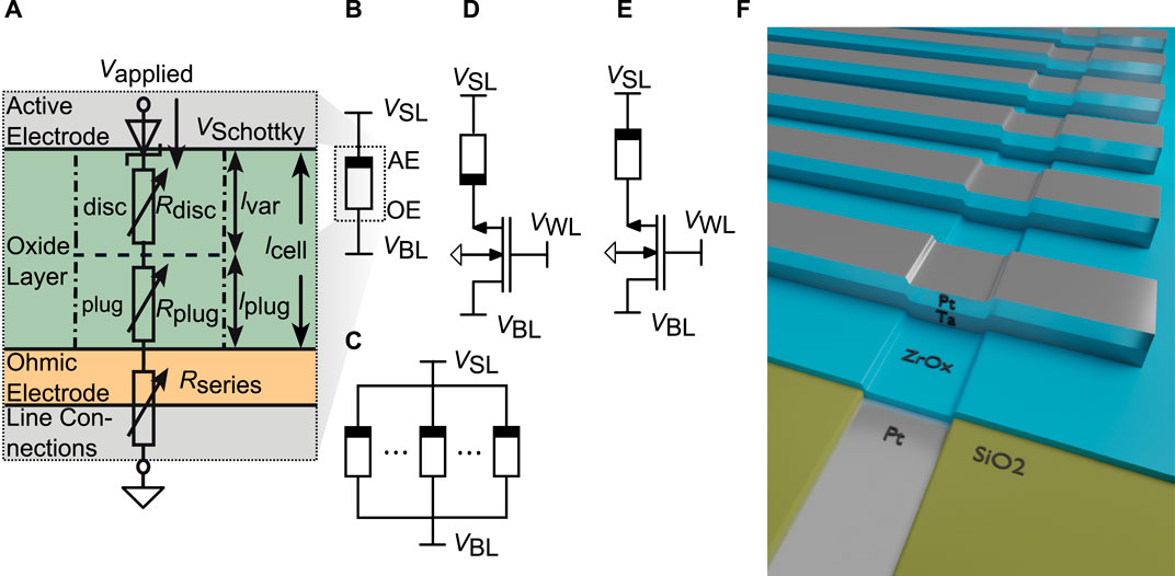
FIGURE 1. (A) Equivalent Circuit Diagram (ECD) of the JART VCM v1b model and the different considered synapse structures (B–F). (B) shows the 1R synapse (C) shows the NR synapse, (D) shows the 1T1R in configuration AE at transistor and (E) shows the 1T1R configuration OE at the transistor. For the synapses containing a transistor the Bulk connections of the transistors are connected to GND. (F) shows the device structure used for the experimental characterization.
Our model has been expanded with a device-to-device (d2d) and cycle-to-cycle (c2c) variability module (Bengel et al. (2020)), which was slightly modified in (Bengel et al. (2021a)) and is used here in the modified version. In the modified version d2d variability can be tuned independently form the c2c variability. The d2d variability is controlled via the variation coefficient varK and the c2c variability can be controlled through c2c% and maximumstepsize. The complete parameter set is taken from (Bengel et al. (2022)), as the same devices were used and it is given in Supplementary Table S1. The only difference is that Rth, SET was increased to 1 ⋅ 106 K/W and Rth, RESET was increased to 8 ⋅ 105 K/W. In this work, the change of the radius of the active region in the filament termed as disc, rdisc, var and the length of the filament ldisc, var are decoupled from the oxygen vacancy concentration change in the disc Ndisc, as opposed to the original JART VCM v1b var model in order to better depict the c2c behavior of the conductance evolution for small concentration changes. With those parameters we could match the experimental characteristics in Section 4. With the parameters fitted to the SET and RESET switching percentages, we generally faced the issue that the d2d variability was too significant to achieve reproducible synaptic behavior. Therefore, we have introduced a new variability parameter set in which we reduce the variation coefficient for the d2d variability to 0.01 and reduce the truncation values of the variability parameters, while keeping the median values the same. The truncation borders were changed to.
•
•
• rfil, var ∈ [25, 35]nm
• ldisc, var ∈ [0.7, 0.9]nm
The c2c variability (c2c%) was not changed. This device can then be viewed as an optimised device with a smaller d2d variability, which should be available in industrial production. For simulations in which additional parameters were modified, we have explained the modifications and the new values in the text.
By utilizing this compact model, the 1R synapse can be realized as shown in Figure 1B, where the VCM cell is connected via the Sourceline (SL) and the Bitline (BL) in the respective crossbar array with the solid rectangle marking the AE. The potentiation is performed, when a positive bias is applied to the BL, while the SL is grounded and vice versa for depression. To simplify matters, the evaluation for the 1R and NR concepts, has been performed by grounding the BL and only applying the negative and positive voltages on the SL to induce potentiation or depression, respectively. Several VCM cells can also be arranged in parallel to form the NR synapse, which is schematically depicted in Figure 1C. This configuration mitigates the shortcomings of the 1R synapse, for instance the poor stability against variability and the small conduction window. The next synapse concept considered in this evaluation is the 1T1R synapse, where an NMOS transistor is connected in series with the VCM cell. The transistor serves as a selection transistor, which removes the sneak path problem as well a the unintentional switching problem occurring in passive crossbar arrays (Zidan et al. (2013)). It can also be utilized to alter the synaptic dynamics of the respective synapse concept. The bipolar VCM cell allows for two possible configurations, namely the AE connected to the transistor shown in Figure 1D and the OE connected to the transistor Figure 1E. The bulk connection of the transistor is set to ground. The choice of the configuration will lead to different synaptic dynamics, since the body effect will either arise during potentiation or during depression.
To characterize the synapse properties experimentally, we fabricated VCM ReRAM cells consisting of a 30 nm Pt/5 nm ZrOx/20 nm Ta/30 nm Pt stack in a 32 × 1 structure with ZrOx representing the switching layer. A schematic of this structure is shown in Figure 1F. The fabrication and measurement procedure are described in the Supplementary Material. Generally, for the experiments shown in Section 4, we use a program verify scheme to initialise the cells in a specific resistance range.
In the past years, many authors have discussed the capabilities of employing various types of filamentary ReRAM devices as synapses and employed different strategies for achieving favourable behavior (Moon et al. (2019); Covi et al. (2016); Vaccaro et al. (2022); Christensen et al. (2022)). One essential characteristic of the memristive artificial synapse is the evolution of the conductance as a function of the applied pulses in time, representing the weight evolution, which will be termed as synaptic dynamics in the following. The weight of the synapse refers to the physical property of the conductance of the synapse, which is normalized between a minimum conductance Gmin and a maximum conductance Gmax. The choice of both values can be quite arbitrary and has to be individually considered for the respective synapse and the chosen operation mode. To update the weight, voltage pulse trains are applied to the synapse terminals to either induce potentiation or depression. Figure 2A schematically depicts different synaptic dynamics. For deep neural network applications based on the backpropagation algorithm, a symmetric, linear weight evolution (orange line) is favoured. However, non-linear synaptic dynamics are typically present (blue, red, green), owing to the intrinsic non-linear kinetics of the VCM cells. In most experimentally reported synaptic dynamics for the 1R synapse, a combination of the red curve for potentiation and the blue curve for depression is seen (Cüppers et al. (2019); Covi et al. (2016); Yang et al. (2020)). However, this is not completely an intrinsic physical property of filamentary VCM devices, but rather also a consequence of the experimental conditions. Intrinsically, i.e. meaning that the experimental conditions affect the device behavior as little as possible, the green curves are a better representation of the device dynamics (Cüppers et al. (2019); Fleck et al. (2016)). As for Spiking Neural Network (SNN) applications, the ideal synapse dynamics might differ. Brivio et al. demonstrated that a SNN based on non-linear synaptic dynamics performs better compared to one based on linear synaptic dynamics in terms of the classification accuracy (Brivio et al. (2021)). The difference between DNN and SNN with regard to the required synapse characteristics has also been studied by (Kim et al., 2021). Kim et al. found SNN to be more tolerant towards non-linear weights. As the main focus of research is based on DNN utilizing error backpropagation during the training, the non-linear synaptic dynamics are often not favored. Still, due to the rapid development of SNNs, it is sensible not to limit the focus of research towards a single type of device behavior. As we will show, through experiment and simulation, different device behaviors can be achieved in the same device, via different stimuli. As part of the synaptic behavior, the bound behavior describes the behavior of the synapse towards the end of the applied pulse train. In the past, various bound behaviors of the synaptic dynamics (Fusi and Abbott (2007); Brivio et al. (2021)) were introduced, which are schematically depicted in Figure 2B for the potentiation. The bound behavior can be classified into a soft bound behavior (blue curve), where the weight value asymptotically approaches a saturation weight value, and a hard bound (red, orange and green curve) behavior, where the dynamics are truncated after reaching a boundary value. Analogously, this behavior is also present for the depression. The bound behavior will also have an impact on the accuracy of the neural network, as shown by Brivio et al. (Brivio et al. (2021)).
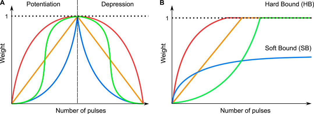
FIGURE 2. Schematic depiction of different types of synapse behavior (A) and different bounding behaviors (B).
In order to analyze and evaluate the behavior of the 1R synapse with respect to its dynamics, it is sensible to introduce certain performance metrics. The literature provides an abundance of information regarding properties of ideal memristive synapses (Xia and Yang (2019); Kuzum et al. (2013); Sung et al. (2018); Fouda et al. (2020); Zhao et al. (2020); Moon et al. (2019)). It should be noted, that not all properties can be fulfilled simultaneously, as the improvement of one characteristic might result in the worsening of another characteristic, which will be discussed more thoroughly in the following sections. Furthermore, the definitions of the “ideal” for some metrics are biased towards DNN application instead of a more open consideration. In this work, we try to take a neutral stance on the performance metrics from the device level perspective. The weight update rules and the synapse evaluation criteria are taken from (Brivio et al. (2021); Fusi and Abbott (2007)). They are shown in Table 1 and will only be discussed here briefly. The fitting procedure used to match the simulation results with the analytical equations can be found in the Supplementary Material. For a quantitative description, weight update rules are chosen from literature, describing the incremental change of the weight dw within an incremental pulse number dn. In practice, dn is set to 1, as discrete pulses are applied. A distinction of the weight update rules can be made with respect to their bound behavior as well as their linearity. For the weight update rules we differentiate between the linear hard bound (L-HB) case and the non-linear soft bound (NL-SB) case. The indices + and − denote potentiation and depression respectively. The L-HB rule is depicted as the orange curve in Figure 2A for the potentiation. α± describes the rate of change and is used as a fit parameter in this work. The pulse stop number Nstop,± is introduced, which describes the pulse number at which the maximum bound is reached (w+ = 1 or w− = 0). A scheme to achieve this kind of potentiation behavior was proposed by Cüppers et al. (Cüppers et al. (2019)) and will be revisited in Subsection 3.1.1. The NL-SB case is shown as the blue line in Figure 2B. In this update rule, a second fit parameter γ± ∈ [1, ∞] is introduced, which contributes to the shape, and thus, the non-linearity of the synaptic dynamics. w0 denotes the initial weight. Non-linear soft bound behavior is the most commonly occurring behavior for filamentary VCM devices (Cüppers et al. (2019); Covi et al. (2016); Frascaroli et al. (2018)). In addition to these update rules, a non-linear hardbound update rule has also been proposed (Brivio et al. (2021)). However, a hardbound in the synapse is generated by external means such as a current compliance limiting the conductance change of the VCM cell. As we use the here defined criteria for the 1R synapse, the focus must lie on properties of the VCM cells themselves, where a hardbound synapse dynamics is not physically sensible.

TABLE 1. Overview of the synapse criteria.
Following the definition of the update rules, we use the quantitatively defined synapse criteria non-linearity, resolution, imbalance, dynamic range and the qualitative criteria variability tolerance. The first performance metric is the degree of the non-linearity, defined as the average radius of the curvature of the synapse dynamics for the potentiation and the depression Brivio et al. (2021). The non-linearity will be analysed in section 3.1.2. The second performance metric, directly related to the non-linearity is the resolution, measuring the number of effective states the synapse can provide Brivio et al. (2021). The resolution will be investigated for the NL-SB case in section 3.1.2. The term effective states covers two aspects. On the one hand the number of addressable states and on the other hand the distribution of the accessible states within the considered dynamic range. When the L-HB and NL-SB are compared, both dynamics exhibit the same number of accessible states given by the number of pulses. For the linear case, however, the conductance change between two pulses is constant, while this is not the case for the non-linear case, where the distinguishable conductance states starts to narrow down when approaching the saturation value. Consequently, for the same range of conductances, linear weight dynamics will have a higher effective number of states compared to non-linear weight dynamics. The third performance metric is the imbalance κ between the potentiation and depression, which is calculated as the mean squared error between the potentiation pulses and the depression pulses. N is the total number of pulses for potentiation and depression. For convenience, the simulation of the synapse dynamics has been chosen in such a way that the potentiation precedes the depression. Hence, the conductance values at pulse n for the potentiation correspond to the conductance values at pulse N − n for the depression. One cycle is defined as one sequence of potentiation and depression. For the imbalance, the normalization of the conductance value is determined by the highest (Gmax) and lowest (Gmin) conductance within each cycle. The imbalance will be quantified in section 3.1.1 and section 3.1.2. While the previous metrics were defined based on the weight, which is a value between 0 and 1, the dynamic range is defined via the conductances. Generally, it is favourable to obtain a large dynamic range at very low conductances, which on the one side provides a proper reading window and on the other side would reduce the power consumption during training and inference. The dynamic range will be analysed in section 3.1.1 and section 3.1.2. While previous concepts are expressed quantitatively, the variability tolerance, is described qualitatively. By using the variability module included in the compact model, it is possible to investigate the effect of d2d and c2c variability. To capture the gradual characteristics of the synaptic dynamics in the presence of c2c variability, the change in the radius of the filament as well as the change in the length of the disc region no longer depend on the oxygen vacancy concentration in the disc region. This implementation ensures a c2c variability throughout the course of potentiation and depression, which is in accordance to the experimental observations (Cüppers et al. (2019); Frascaroli et al. (2018). The variability tolerance will be investigated for every synapse concept in the following sections.
The 1R synapse forms the basic resistive synapse concept. The synaptic dynamics solely depend on the physical processes governing the VCM cell and the experimental conditions. One can distinguish between a strong programming and a weak programming mode, which are both depicted in Figure 3 for potentiation (A and B) and depression (C and D) simulation, respectively. In Figure 3A, the strong programming is shown for the SET, which involves a single pulse of −600 mV for tSET = 1 m. The initial conductance state and the pulse amplitude are chosen to have a good resolution of the transition region during the applied pulse. After a certain delay time tdelay, the SET starts at around 380 µs? In Figure 3B a weak programming is shown, where a partial conductance increase is obtained by applying a SET pulse train with tSET = 10 µs for 100 pulses at the same voltage amplitude. The conductances in both cases are evaluated at the same voltage because of the device non-linearity. As we did not want to interrupt the strong programming pulse, the reading voltage was chosen as the SET voltage. In the weak programming case, the conductance was evaluated at the end of each weak programming pulse. The strong and weak programming scheme also applies for the RESET, which is shown in Figures 3C, D, respectively. In these cases, the RESET pulse amplitude was 800 mV.

FIGURE 3. Simulated strong and weak programming of the VCM device. The transient obtained for one single pulse can be can be divided into a corresponding pulsed conductance evolution by utilizing weak programming. (A) Strong programming transient of a SET obtained for one pulse at −600 mV for tSET = 1 ms. (B) Weak programming pulse equivalent of the SET transient by utilizing a pulse train with
While the strong programming is associated with a large, binary change of conductance, where the whole dynamic range of the VCM device is traversed within one single pulse, weak programming induces gradual conductance changes by performing pulse operations with pulses on a smaller time scale. Thereby, an approximation can be made, where the conductance change induced by a single pulse is equivalent to N incremental pulses with a pulse width being
It is now possible to distinguish between three different trends of synaptic dynamics by providing a proper truncation of the dynamic range, which based on their underlying physical principles are termed as the delay regime, linear regime and saturation regime (Figure 3). While the conductance range for the gradual regime remains the same, the delay regime and saturation regime are reversed for potentiation and depression, e.g. the delay regime for potentiation starts within the LCS of the VCM cell, and conversely the delay regime of the depression starts within the HCS. In the following two subsections we will discuss the linear and saturation regime in more detail. The delay regime which describes the LCS behavior in the potentiation and the HCS behavior in the depression direction is not considered as in most literature studies focusing on synaptic behavior. For this there are several reasons such as the difficulty to address the regime in a controlled fashion. Especially in the potentiation direction the thermal runaway can not be prevented reliably. Additionally, for the potentiation, the range of the delay regime strongly depends on the LCS which is known to suffer more from inaccuracies such as read noise Wiefels et al. (2020).
A linear synaptic dynamic, both for potentiation and depression, can be achieved by exploiting the switching kinetics of the VCM device. Cüppers et al. have already performed an extensive study on this matter and this subsection will be based on the concepts introduced in their work (Cüppers et al. (2019)). The switching kinetics itself refer to the exponential relationship between SET/RESET time and the applied voltage, where a linear change in the applied voltage leads to an exponential change of the switching time. The switching time itself can be split into the delay time, dependent on the initial state, describing the time until the onset of the SET/RESET event and the transition time, independent of the initial state, which marks the time interval in which the conductance changes abruptly Cüppers et al. (2019). These times are defined based on the definition of the conductance window for the linear regime, truncating delay and saturation regime. A theoretical tool to help in the analysis is the dynamic route map (DRM) (Chua (2018); Ascoli et al. (2018); Marrone et al. (2022)), which tracks the change of the state variable over time. This theoretical concept has already been successfully applied to describe the switching characteristics of ReRAMs (Maldonado et al. (2020); Ascoli et al. (2022)) and PCM (Marrone et al. (2022)). In the deterministic view, the DRM (as the transition time) is independent of the initial value of the state variable. On the other hand, the delay time shifts to higher values when the initial conductance state is decreased (SET) or increased (RESET). The delay time itself arises from the fact, that the self accelerating temperature and field contributions of the voltage pulse need a certain time to reach the runaway point. For the SET, a decrease of the oxygen vacancy concentration leads to a larger voltage mainly across the Schottky contact, whereas for the RESET, when the concentration is increased, the voltage drop will mainly be across the series resistance. Both of these model elements do not contribute to the respective electric fields driving the ionic current.
Using the insights provided by the DRM, the conductance window for the gradual regime can be further narrowed down. The goal here is to maximize the dynamic range in the linear region without loosing too much symmetry between the SET and the RESET by including the delay or saturation regimes. Under these requirements, the linear window has been determined to
FIGURE 4. Simulations of the synaptic dynamics of the linear regime (A) with its calculated normalized DRM (B). (C) shows the simulated effect of d2d variability on the conductance evolution during potentiation and depression, within the linear regime. (D) shows the simulated deterioration of the operation in the linear regime due to the c2c percentage. For (C) and (D) we used the optimized device with reduced d2d variability (section 2.1). Simulations of the cyclability of the linear regime for the case of a slightly too strong SET operation (E) resulting in a decreased dynamic range and a reduced imbalance (F).
Since the achievable dynamic range is truncated between Glinear,min and Glinear,max, to provide the linearity, this results in
Next, the synaptic dynamics in the saturation regime are considered. In Figures 5A, B, the synaptic dynamics for the potentiation and depression are shown for pulse trains of different pulse voltages for a pulse length of 1 μs The VCM cell is initialized at the conductance values Glinear, max = 3 mS for potentiation and Glinear, min = 2 mS for depression. Those values are read out at −0.1 V to be consistent with the ranges in Figure 4. Due to the initialization, we are purposefully excluding the linear region to characterize only the saturation part of the dynamics. This has of course an effect on the synapse evaluation criteria such as the dynamic range which will be smaller as large parts of the conductance change happen in the linear region. In the experiment, this precise differentiation is not possible due to the variability. The trends of the synaptic dynamics upon receiving an increased pulse voltage is the same in Figures 5A, B. The conductance evolution shows a small but linear change over the course of the pulse train for small voltages and becomes less linear upon receiving higher pulse voltages. The term saturation relates to the asymptotic approximation of a certain conductance value for an infinite number of pulses. This description also coincides with the definition of the soft bound behavior of the synaptic dynamics. For the potentiation, the saturation conductance value is equivalent to the HCS of the VCM cell, while for the depression, the LCS would be achieved. Since we considered here the deterministic case with our simulation model, LCS and HCS will be determined by the median values for Ndisc, min, var and Ndisc, max, var, for high enough voltages.
FIGURE 5. Simulated synaptic dynamics of the saturation regime of the 1R synapse for different applied pulse voltages for (A) potentiation and (B) depression. The voltages in potentiation direction were between −0.4 V and −0.9 V with 25 mV steps and the voltages in depression direction were between 0.4 V and 1 V with 50 mV steps. The VCM cell is initialized at Glinear, min = 2 mS (for depression) and Glinear, max = 3 mS (for potentiation). The corresponding dynamic ranges, non-linearity and resolution are shown in (C) for potentiation and (D) for depression. In (E) and (F) we have simulated ten potentiation and depression curves with the variability of the improved device as explained in section 2.1. The deterministic curve is shown as the thicker black curve. The potentiation voltage was −0.5 V and the depression voltage was 0.8 V.
Figures 5C, D shows the performance metrics dynamic range ΔG±, non-linearity λ± and resolution η±. The dynamic range for the potentiation direction is capped at around ΔG+ = 1.53 which is given by the series resistance serving as an inherent limit, given that the disc is becoming more and more conductive. This is different for the depression direction, where the dynamic range can reach ΔG− > 5, since the disc resistance contributes the most to the overall conductance in the low conductive regime. Consequently, the VCM cell can be further RESET, as long as the field and temperature contributions are sufficient to drive the ionic oxygen vacancy current. As indicated in the introduction of the performance metrics, both the resolution and the linearity are interdependent. A high resolution is characterized by a low non-linearity. This case is typically achieved for small voltages, however, the dynamic range is significantly reduced, as only marginal oxygen vacancy changes occur. For higher voltages, the resolution decreases and the non-linearity increases. For sufficiently large voltages in both potentiation and depression direction, the resolution becomes η± = 2, which represents a degradation into the binary case. Figures 5E, F each show ten exemplary potentiation and depression curves with the variability parameters of the optimised device (section 2.1). The potentiation voltage was 0.5 V and the depression voltage was 0.8 V. The deterministic curve is shown as the thicker black curve. The different initial conductances are an effect of the d2d variability, the noisiness of the different curves is a consequence of the choice of c2c variability.
Similarly, instead of adjusting the pulse voltage, the pulse width can be changed. A summary of the performance metrics resolution η±, non-linearity λ±, and dynamic range ΔG as a function of the pulse width and voltage is provided in Figure 6. These performance metrics are obtained for a pulse train consisting of 100 pulses. Note, that the pulse width is plotted on a logarithmic scale. Starting with the resolution shown in Figure 6A for potentiation and Figure 6B for depression, the voltage asymmetry between both directions is visible. Furthermore, the non-linear kinetics governing the device can also be seen: while changing the pulse widths achieves a similar effect as with changing the pulse voltage, in order to traverse the resolution range, the pulse width has to change orders of magnitude, whereas the same effect can be accomplished adjusting the pulse voltage by a couple hundred of millivolts. The interdependence between the non-linearity shown in Figure 6C and Figure 6D and the resolution is also clearly visible. The dynamic range in the potentiation direction, shown in Figure 6E, reveals the maximum obtainable dynamic range capped at ΔG = 1.53, originating from the inherent limit of the series resistance, whereas in Figure 6F, the dynamic range can become much larger. The more abrupt behavior of the dynamic range for the potentiation direction can be explained via the device physics as well. At low voltages and short pulse lengths the device is barely switching at all. As soon as the combination of pulse length and amplitude is sufficient, however, the switching self-accelerates as explained in section 2.1. The series resistance represents then the upper bound for the dynamic range. In the depression direction this upper bound exists as the drift requires ever higher voltages to accelerate the ionic movement. Therefore, at each voltage, a minimal conductance exists, which will be approached for the longer pulse lengths. The saturation characteristics of the VCM cell and the associated soft bound behavior is a commonly observed feature of VCM based cells and has been experimentally verified by earlier works Frascaroli et al. (2018). The simulation results depicted here demonstrate that the soft bound nature of the 1R synapse can be explained by the compact model and shows an adequate match to the experimental data. The maximum dynamic range for the potentiation is considerably smaller compared to the maximum experimental dynamic range, which is around ΔG = 5. The reason for this deviation lies in the separated investigation of the respective regimes provided here as mentioned above. While it is sensible to exclude the delay regime, the saturation regime can also be well depicted, when the linear regime is included for both potentiation and depression. The initialization values will thereby shift towards Gtrans, min = 0.26 mS for potentiation Gtrans, max = 0.35 mS for depression. For potentiation, this would enable a dynamic range of ΔG+ = 2.5. To summarize the results from the saturation regime, it is important to consider multiple evaluation criteria as improvements made for one might result in worsening of another. For the criteria which we investigated, this is for example the case if one tries to increase the dynamic range which leads to an increased non-linearity. Another example of this trade off is the relationship between the resolution and the dynamic range.

FIGURE 6. Parameter study involving the variation of the pulse width and pulse voltage and its effect on the performance metrics: Resolution η± for (A) potentiation and (B) depression, non-linearity λ± for (C) potentiation and (D) depression, dynamic range ΔG± for (E) potentiation and (F) depression. The results were obtained by fitting the analytical equations in Table 1 to the deterministic simulation results.
Extending the 1R synapse concept by using multiple cells in parallel, one reaches the NR synapse. This concept has been explored in the past in detail and exploits the intrinsic variability of ReRAM devices (Bengel et al. (2021a); Garbin et al. (2015); Gaba et al. (2013)). It has also been demonstrated for other memristive devices like Phase Change Memory (PCM) (Boybat et al. (2018b)). In this work, we will focus on how to operate a NR synapse based on VCM cells in order to achieve different switching and thereby synaptic dynamics. Commonly, the individual devices in the NR synapse are switched in a binary fashion. This leads to the wanted gradual synaptic dynamics, as the switching process is stochastic, in the way that there exists a voltage range in which the devices have a certain probability to switch upon receiving a programming pulse. This probability can be included in a stochastic gradient descent algorithm, in which the switching probability is coupled to the error of the neural network classification (Bengel et al. (2021b)). By applying multiple constant voltage pulses, the NR synapse can be made to change rather gradually, as individual devices are switching one after another. We have shown in the past, that the origin of the stochastic voltage range, in which all devices are switched, mainly originates from the d2d variability of the VCM cells, while c2c variability is less significant (Bengel et al. (2021b)). The stochastic voltage ranges are depicted in SET and RESET probability curves (Dalgaty et al. (2019); Singha et al. (2014); Bengel et al. (2021a)). While the SET exhibits an abrupt characteristic stemming from the positive feedback between the temperature and the field acceleration of the oxygen vacancy movement, the RESET typically shows a more gradual nature, due to the negative feedback of reducing current and heat. However, by initializing the VCM cells in a sufficiently high HCS, determined by the internal series resistance, an abrupt RESET can be achieved (Cüppers et al. (2019); Hardtdegen et al. (2018; 2016); Strachan et al. (2013)).
In this work, we are not operating the NR synapse with constant voltage pulses, but with voltage pulses increasing in amount for the potentiation and depression direction. The aim is to reproduce the synaptic dynamics delay regime, linear regime and saturation regime of the 1R synapse with the NR synapse. Under a constant voltage pulse this could be done by using the weak programming idea as for the 1R synapse, but it will suffer from the same challenges that were discussed in Section 3. With the increasing voltage pulses this can be achieved as we will show in Subsections (4.3 and 4.4) by adapting the start and end voltages of the pulse train on the switching probability curve. We will first explore the potentiation and depression behavior as a function of the d2d and c2c variability, based on which we will explain our concept for achieving different synaptic dynamics (section 4.1). We will then characterize the experimental SET and RESET probabilities from our fabricated devices and show that they are in a good match with our compact model (section 4.2). In the end, we will experimentally and through matched simulations demonstrate the different synaptic dynamics (sections 4.3, sections 4.4 and sections 4.4).
The concept we have proposed is based on using the SET/RESET switching probabilities, which strongly depend on the LCS/HCS of the device (Cüppers et al. (2019)). To achieve a symmetric potentiation and depression, but also to perform multiple potentiation and depression cycles after one another (cyclability), its crucial to start from well defined resistances and arrive at specific resistances, respectively. This means, that the conductance variability of the HCS and LCS after the pulse train should be as small as possible. Figure 7 showcases the behavior of the NR synapse for N = 8 devices at different amounts of d2d and c2c variability A-D. In Figure 7E, we qualitatively show how the complete conductance evolution curve of the NR synapse can be split into the three conductance dynamic regimes and Figure 7F shows the controlled operation in the linear regime. As introduced in (Bengel et al. (2021a)), d2d and c2c variability can be tuned independently from each other. This can be done by changing the variation coefficient (varK), of the distributions from which the parameters are initially drawn for the d2d variability, or by changing the percentage, by which the parameters can change around the initially drawn values (c2c%), for the c2c variability.
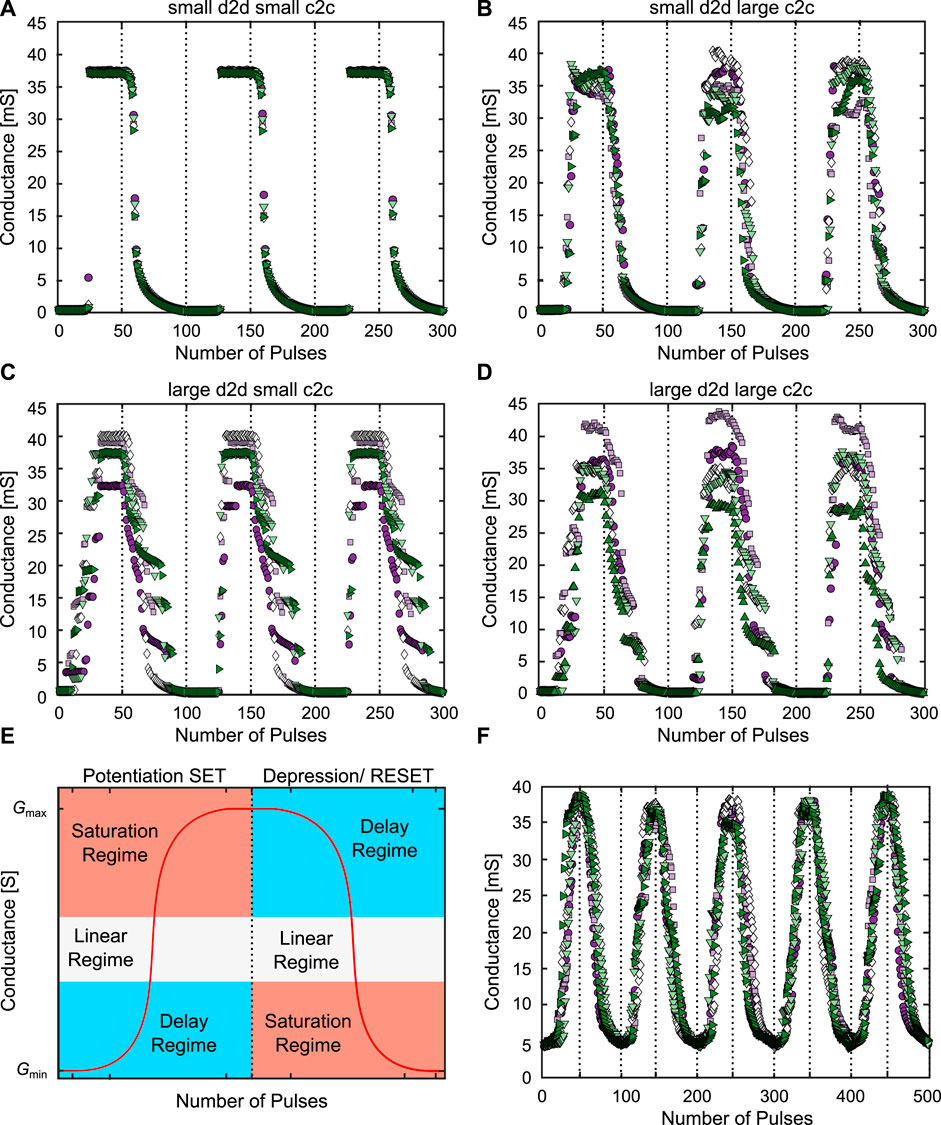
FIGURE 7. (A–D) show the synaptic dynamics of the NR synapse for different amounts of d2d (varK) and c2c (c2c%) variability. For (A) (varK/c2c%) are (0.01/1%), for (B) they were (0.01/30%), for (C) they were (1/1%) and for (D) they were (1/30%), respectively. In (E) we show how the conductance evolution can be split into the three conductance dynamic regimes. (F) shows the controlled pulse operation in the linear regime for the device with reduced d2d variability. In all these simulations N was chosen as 8, and five 8R synapses were simulated for three ((A–D)) or five (F) SET/RESET cycles.
In Figure 7A, the d2d and c2c variability are small, in Figure 7B d2d stays small while c2c is large, in Figure 7C d2d is large while c2c is small and in (d) both variability’s are large. Figure 7D then has the same values as the parameter set which was fitted to our own devices. In A to D we applied a voltage pulse train for SET and RESET consisting of 50 pulses with an absolute increasing amplitude between ∣0.4 V∣ and ∣2 V∣. We started at small voltages at which no switching is observed and ended at voltages at which all devices are switched. In this way it was possible to show the typical ‘S’ shape of the complete conductance evolution (Bengel et al. (2022); Dalgaty et al. (2019); Zahari et al. (2020)). This was repeated five times for eight different devices each time and for three potentiation/depression cycles, each to observe the repeatability of the behavior. For the case of the small d2d and c2c variability A, as expected the five different synapses almost all behave the same over the course of the three cycles. As the devices are almost identical, initially they slowly change their conductance and then they all abruptly switch at the same SET voltage after which they stop switching, as the maximum HCS is reached. In the RESET direction, at first the conductance is changing slowly as well, followed by a more abrupt regime, between around 35 mS and 10 mS, which transitions into a gradual and slow conductance change for the rest of the pulse train between 10 mS and ≈0 mS. Those three regimes observed for eight VCM devices in parallel, correspond to the delay, linear and saturation regime, observed for the 1R synapse, as the devices in A are still very deterministic. While the RESET already shows an addressable linear regime, the SET directly transitions from the LCS to the HCS, without any intermediate steps. Even for the RESET, most of the pulse train is not spent in the linear regime, but in the slowly changing saturation regime. Of the 50 pulses, only around five are part of the linear regime. Due to their different switching behaviors, SET and RESET are also not symmetrical. In conclusion, the NR synapse with small d2d and c2c variability suffers from the same limitations as the 1R synapse.
By adding c2c variability to the VCM devices we arrive at Figure 7B. Here, we can identify several significant differences to Figure 7A. For example, the HCS variability is increasing, which makes it more difficult to achieve a reproducible RESET behavior between the five simulated synapses. This variability also reduces the reproducibility of the RESET over multiple cycles, as the RESET pulse train begins at a wider range of different initial conductances (30 mS to 40 mS). Another feature is that the SET now has a stochastic switching window, in which not all devices have switched to the HCS. This also leads to a higher symmetry between SET and RESET. For the RESET, the stochastic window has slightly widened, in both the horizontal (number of pulses) and the vertical (conductance range) direction. Increasing the d2d variability instead of the c2c variability, we arrive at Figure 7C. One important difference here is that the second and third cycle are very similar to each other due to the small c2c variability. This shows a very good cyclability of the synapse, but it is physically unreasonable to assume that devices would be possible with a large d2d and small c2c variability due to the stochastic nature of the VCM mechanism. The first cycle is different from the second and third cycle, mostly on the SET side, as the devices are initialised before the first cycle, but afterwards their conductance is a result of the programming pulses. The HCS is again characterised by a high variability. The stochastic SET window is similar to Figure 7B, but the RESET side has changed significantly, exhibiting a ladder like behavior. This can be explained by the freezing in of the relative device properties such as the switching speed. The freezing in is a result of the small c2c variability. By relative device properties we mean how an individual device behaves in relationship to the other devices, e.g. at which voltages it switches to which resistances. With c2c variability these relative device properties change over time, however by removing the c2c variability slower device will stay slow and fast devices will always be faster. This leads to the reproducible (between different synapses) and repeated (over multiple cycles) ladder like behavior. While both SET and RESET have a clear stochastic window, they are not symmetrical in this case, due to the ladder like behavior on the RESET side. Figure 7D shows the same simulation for the case of a large d2d and c2c variability, which was fitted in (Bengel et al. (2022)) to a range of different SET and RESET kinetic experiments. Opposed to the results in A to C, the stochastic window in the SET direction is larger. The HCS variability is similar to Figure 7B but even stronger, with the HCS ranging from 30 mS up to 45 mS. The ladder like behavior of the RESET is visible, but less pronounced than in Figure 7C. By restricting the voltage range, we can now control the shape of the SET and RESET direction. Figure 7E schematically shows, how to split the conductance evolution into the three conductance dynamic regimes. The red curve shows the typical ‘S’ shape of the idealised 1R and NR synapse conductance evolution. By cutting out slices of the conductance evolution according to the different colored areas in Figure 7E, the different synaptic dynamics can be realised. Figure 7F shows the addressing of the linear regime over five SET/RESET cycles. In this simulation, we have used the optimised device with reduced d2d variability (section 2.1). To only access the linear regime, the voltage range was reduced to −0.55 V to −0.65 V for the SET side and 0.6 V–0.8 V for the RESET side while still using 50 pulses for both SET and RESET. Through this reduction it is possible to extend the stochastic switching range over almost the full 50 pulses of SET and RESET and to achieve a very symmetric SET and RESET operation. This reduction of the voltage range also leads to an increase of the LCS while the HCS does not change strongly. The reproducibility of the SET and RESET is very good, which can be attributed to the tightly controlled conductance states at the end of the SET/RESET pulse trains. In summary, we have shown here how either d2d or c2c variability is required to achieve all three possible synaptic dynamics of the NR synapse. Those regimes are analogous to the 1R case, but here they can be achieved reliably.
As we have shown here, by restricting the voltage range, the synaptic dynamic of the NR synapse can be shaped to only be a certain part of the total ‘S’ shape dynamic. The restriction of the voltage range is defined via the SET/RESET probabilities. Therefore, before showing all three dynamics we will characterize the switching probabilities in the next Subsection.
Before the stochastic switching can be exploited, it has to be characterized experimentally and described through simulation. For the experimental characterization of the SET and RESET probabilities, we considered N = 8 VCM devices in parallel to each other, to closely match the measurements on the NR synapse. We first programmed each device individually to the LCS range for the SET direction and to the HCS for the RESET direction. The high resistance range (= low conductance range) is defined as 30 kΩ ± 30% for each individual cell, while the low resistance range (= high conductance range) is defined as 1 kΩ ± 30% for each cell. In the simulations, the devices were also initially programmed to the same target conductance range, to be as close as possible to the experiment. Then, the SET/RESET voltage is applied to N cells simultaneously with a 100 μs long pulse. Voltages between |0.4 V| and |2.2 V| were tested in 50 mV steps. Finally, the conductivity of each device is measured with a −0.1 V pulse, low enough to not further alter its state. If the devices were found to be outside of the initial resistance range they were programmed back and the measurement was repeated with a different voltage. The choice of the next voltage was randomized in order to prevent accumulative effects (gradual switching). The criteria for a successful SET and RESET operation are not defined based on the crossing of a single threshold conductance value. Instead, the thresholds are defined as the conductance value for which the respective initial conductance has doubled (in the SET direction) or halved (in the RESET direction). In this way, there is a direct relationship between the switching probabilities and the synaptic dynamics, as the switching probability relates to a certain amount of conductance change, which is symmetrical for SET and RESET.
Figures 8A, B show the experimental results for the SET and RESET probability. A 95% confidence interval obtained via bootstrapping (DiCiccio and Efron (1996)) is also given. To derive it, a number of samples is randomly drawn from the experimentally observed distribution of successful/unsuccessful SET attempts (for each voltage), that is equal to the number of measured data points. This is repeated 5,000 times, and each time the set percentage is determined. From this the confidence interval can be estimated. For most voltages, the percentages are calculated from at least 50 measurements, taken on
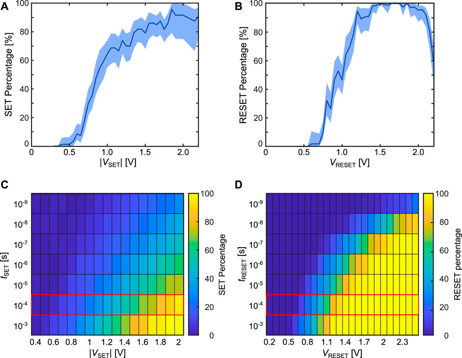
FIGURE 8. (A, B) show the experimental SET and RESET percentages for different applied voltages. The shaded area indicates a 95% confidence interval for the probabilities. The experiments where done for a pulse length of 100 μs. (C, D) show the simulated SET and RESET percentages for a range of pulse durations and different voltages as a heat map. The red rectangles around the 100 μs indicate the same pulse length as in the measurements.
Figures 8E, F show the simulation results for the SET and RESET percentages at different voltages and for different pulse durations, respectively. To account for the device variability, 100 cells were simulated at each combination of voltage and pulse length for one voltage pulse. In this way, the simulation only displays the d2d variability which has been shown to be the main contributor to the stochastic switching (Bengel et al. (2021b)). As expected, higher absolute voltages, as well as longer pulse durations increase the respective probabilities. The stochastic switching window then describes the range of voltages for which the switching percentage is
The voltages to achieve the different synaptic dynamics can now be determined. For the delay behavior, one has to start at a voltage corresponding to a probability of around 0% or at smaller voltages and increase it towards roughly 100%. For the linear behavior, one has to start at a percentage slightly above 0% and increase it towards 100% and for a saturation behavior one has to start above 0% and end at a voltage higher than the 100% voltage. Due to the fact that a concrete synapse of N devices might not have the same switching percentages that were measured on a larger subset of devices, the optimum voltages might not exactly correspond to the switching percentages, but the voltages were chosen through this approach in the next two Subsections.
Based on the measurements and simulations of the SET probabilities as a function of the applied voltage, we then applied pulse trains according to Figures 8A, C to achieve delay, linear and saturation type dynamics. The results are shown in Figure 9 with the experimental results on the left side (A, C and E) and the equivalent simulations on the right side (B, D and F) for N = 8. The conductances shown are the conductance of eight VCM devices in parallel. In each regime, ten experimental runs and ten simulation runs were performed with eight devices in each case. For the potentiation and depression experiments, pulse trains with 20 pulses were chosen due to the limitations of the measurement setup as not arbitrarily small voltage differences (
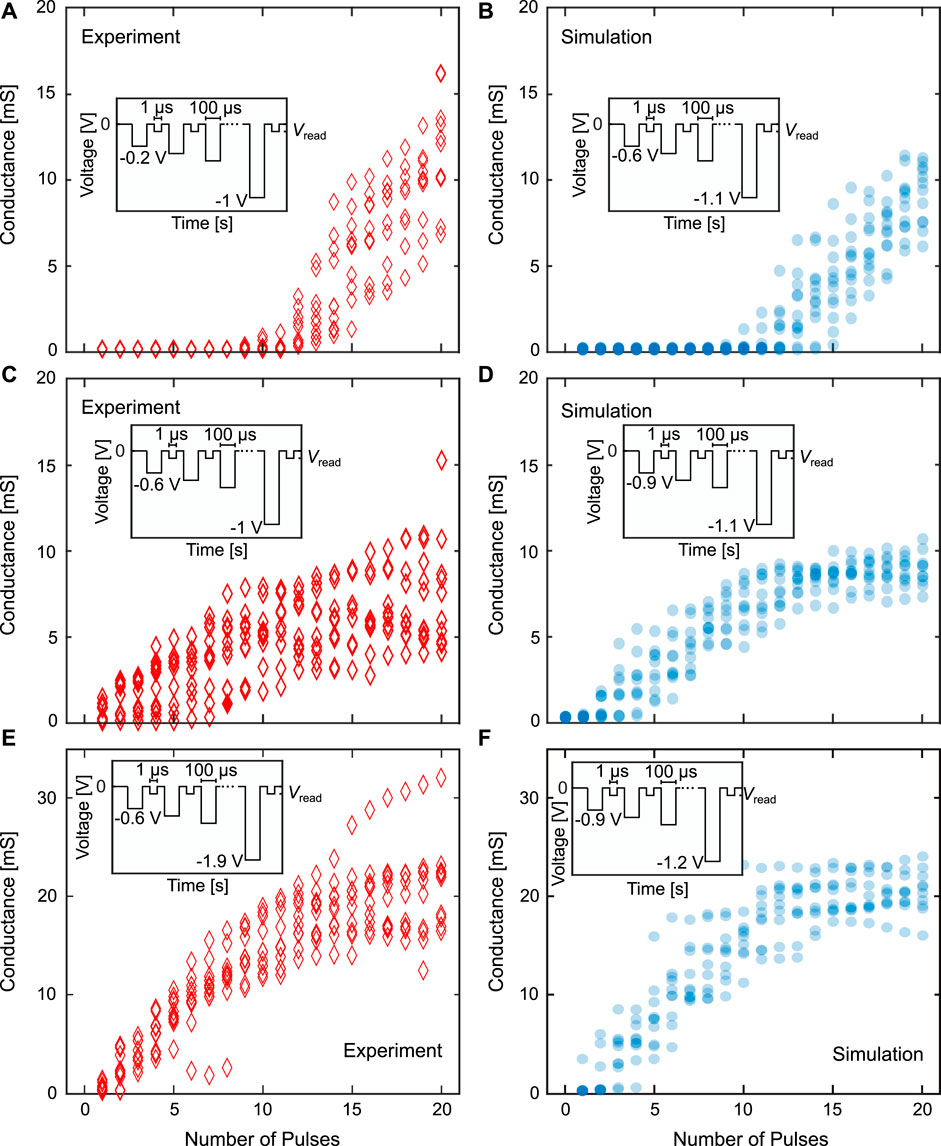
FIGURE 9. Comparison of the delay regime (A) and (B), the linear regime (C) and (D) and the saturation regime (E) and (F) between experiment (left) and simulation (right) for the potentiation or SET direction and for N = 8. The conductances shown are the conductance of the complete synapse. The insets describe the pulse schemes with the applied voltages and pulse lengths.
The delay regime (A and B) is characterised by an initial, near-constant conductance during the first pulses as the applied voltage is to small to lead to any switching. Thereafter, the conductance gradually increases. The length of the initial non (or very weak) switching region can be controlled by the part of the voltage pulse train which is at voltages for which the SET percentage is around zero percent. While there is a small horizontal shift between the onset of the gradual change between experiment and simulation, the conductance ranges are very similar. For the linear regime (C and D) the aim is to achieve a gradual conductance tuning over the whole pulse train. Therefore, the devices have to start switching during the first few pulses and have to keep on switching until the end of the pulse train. The conductance variation as well as the final conductance range of around 5 mS to 10 mS are well matched. The linear regime is the regime with the smallest voltage range, as the voltage has to be high enough to not exhibit a delay regime behavior and low enough, to not go into the saturation regime. For the saturation regime (E and F), the aim is to first achieve a gradual tuning of the conductance, which then reduces its slope until the conductance does not change any further. To this end, one starts at relatively high voltages, to directly start switching, the same as in the linear case. The voltage at the end of the pulse train has to be chosen higher than in the linear range. The pulse number at which the conductance change starts to level off, roughly corresponds to the voltage level, where the SET/RESET percentage reaches 100%. In reality, the conductance starts to level of already earlier as the devices are already in a potentiated state, which increases their SET probability as explained in section 4.2. For the corresponding simulations, the parameter set had to be slightly adapted to better match the synaptic dynamics. One change was that the variation coefficient determining the d2d variability had to be reduced to 0.1, as otherwise the curves would have shown a too large variability. The original parameter set was therefore overestimating the variability and had to be reduced in order to better match the experiment. Additionally, to match the conductance at the end of the voltage pulse train, the median values of the distribution for the maximum oxygen vacancy concentration (Ndisc, max, var) were adapted individually for each dynamic regime. They are 4⋅1026
For the depression direction, we use the RESET probabilities to determine the appropriate voltage ranges for delay regime, linear regime and saturation regime. The conductance evolutions, pulse schemes and used voltage ranges are shown in Figure 10 with the experimental results again on the left side (A, C and E) and the equivalent simulations on the right side (B, D and F). In analogy to the potentiation direction, ten experimental runs and ten simulation runs were performed in each regime. For the depression direction, the delay regime (A and B) also shows a near constant conductance due to a very weak switching. After a specific voltage pulse, which corresponds to the voltage at which the cells start to switch stochastically, the conductance decreases until the final pulse. This behavior is quite well matched by the simulations in terms of the amount of variability and the range of conductances after the final pulse. For the linear regime (C and D) the goal is again to achieve a gradual conductance tuning over the whole pulse train, which can be achieved quite well in the depression direction. The curves also agree well between experiment and simulation. For the saturation regime (E and F) one should transition from a gradual change of the conductance to a region in which the conductance stays constant. This is actually harder in the RESET direction, as the conductance still slightly changes, even after the saturation regime is reached (around pulse 12). While in the potentiation direction, the internal series resistance will limit the switching as soon as the device resistance approaches the series resistance, the final conductance value in the depression direction is not affected by this series resistance. This feature is also matched by the compact model. As in the SET direction we also reduced the variation coefficient, to a value of 0.2.
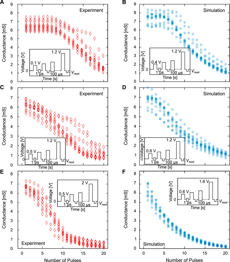
FIGURE 10. Comparison of the delay regime (A) and (B), the linear regime (C) and (D) and the saturation regime (E) and (F) between experiment (left) and simulation (right for the depression or RESET direction and for N = 8. The conductances shown are the conductance of the complete synapse. The insets describe the pulse schemes with the applied voltages and pulse lengths.
To summarize, the NR synapse is a convenient concept to deal with the inherent variability present in the VCM cell and allows for different, gradual operation modes. Comparing it to the behavior of a single device, especially, the stabilization of the three regimes is of great interest. Regarding the relationship between the switching probabilities and the choice of the voltages for the three dynamic regimes it should be noted that the switching probabilities were measured and simulated for a larger number of devices (50 in experiment and 100 in simulation) when compared to the results for the synaptic dynamics (8 devices in both cases). As the initial conditions before the SET or RESET pulse are of great importance, it might be useful to introduce a write-verify process to bring the devices into the wanted conductance states. If those initial conductances can be controlled, different types of dynamics can be achieved over many cycles and different synapses.
As passive crossbar configurations suffer from issues such as sneak paths during read out or from resistance drift during programming, transistors can be introduced in series to the VCM cells, which leads to an active 1T1R structure. 1T1R arrays are today practically the standard for neuromorphic applications (Garbin et al. (2015); Milo et al. (2021); Yao et al. (2020); Xue et al. (2020)) as they allow for the programming and readout of each individual cell without disturbing neighbouring cells. In 1T1R arrays, mainly NMOS transistors are used, as they offer a higher charge carrier mobility at the same transistor dimensions compared to PMOS transistors, which leads to a smaller footprint of the 1T1R cell and thereby reduces the footprint of the whole array. The Bulk connection of all transistors is connected to Ground. This means, that negative voltages cannot be used, as otherwise the Bulk to Drain or the Bulk to Source diodes could become conducting. When considering the 1T1R element, there exist two possible configurations for the wiring, as either the AE or the OE can be connected with the transistor, as detailed in Figures 1D, E. As we will show in the following, these two configurations lead to different synaptic dynamics. Considering the configuration where the AE is connected to the transistor, Figure 1D, potentiation is performed by applying a positive voltage to the WL and SL, while grounding the BL. In this configuration, the gate source voltage VGS of the transistor during the depression, depends on the state of the VCM cell according to VGS = VG, RESET − VVCM. Additionally, the body effect arises due to the potential difference between the source and bulk, which results in a shift of the threshold voltage of the transistor. For the potentiation direction, the source is connected to Ground, hence VGS = VG, SET. If the OE is connected to the transistor, the functions of BL and SL are inverted and the body effect will arise for the potentiation. For the read operation, the gate voltage VG, READ is used and VREAD is applied such that the body effect is avoided.For the evaluation, a 130 nm technology node SPICE-based BSIM4 NMOS model card is utilized (Nanoscale Integration and Modeling (NIMO) Group at ASU (2006)). If not specified otherwise, the pulse width for potentiation and depression are kept constant at tpotentiation = tdepression = 10μs. For the simulations with variability, the variability parameters here represent the reduced d2d variability device, as introduced in Subsection 2.1.
The addition of the transistor complicates the evaluation of this synapse concept, since the weight dynamics no longer solely depend on the physical behavior of the VCM device, but also on the behavior of the transistor. A convenient way to illustrate the interplay between the VCM cell and the transistor is provided by adapting the load line concept, a well known graphical analysis tool in electronics. In Figure 11A the auxiliary circuit is shown, with which we simulated the transfer characteristic (TC) of the PTM 130 nm transistor model without the body effect (no b. e.). Figure 11B shows the schematic to simulate the TC with b. e. Since VCM cells are bipolar devices, we need to drive the 1T1R synapse from both directions, SL and BL. In one direction, VGS will be a function of the resistance of the VCM cell, which increases VS. Figure 11C shows the two possible connection cases of the 1T1R synapse with the potential definitions for SET/potentiation (cases 2 and 3) and RESET/depression (cases 1 and 4). If the AE is connected to the transistor (AE configuration), the b. e. is observed in the RESET direction (case 1), while it is observed in the SET direction (case 3), if the OE is connected to the transistor (OE configuration). The resulting TCs are shown in Figure 11D for the Gate voltages 0.5 V, 1 V, 1.5 V and 2 V. The transistor dimensions are W = 260 nm and L = 130 nm. The simulations without the b. e. are shown in yellow, while the simulations with b. e. are blue. Without b. e. the TC shows the typical behavior with a transition from the linear regime to the saturation regime. With b. e. the transistor is either off, or in the saturation regime since VGS
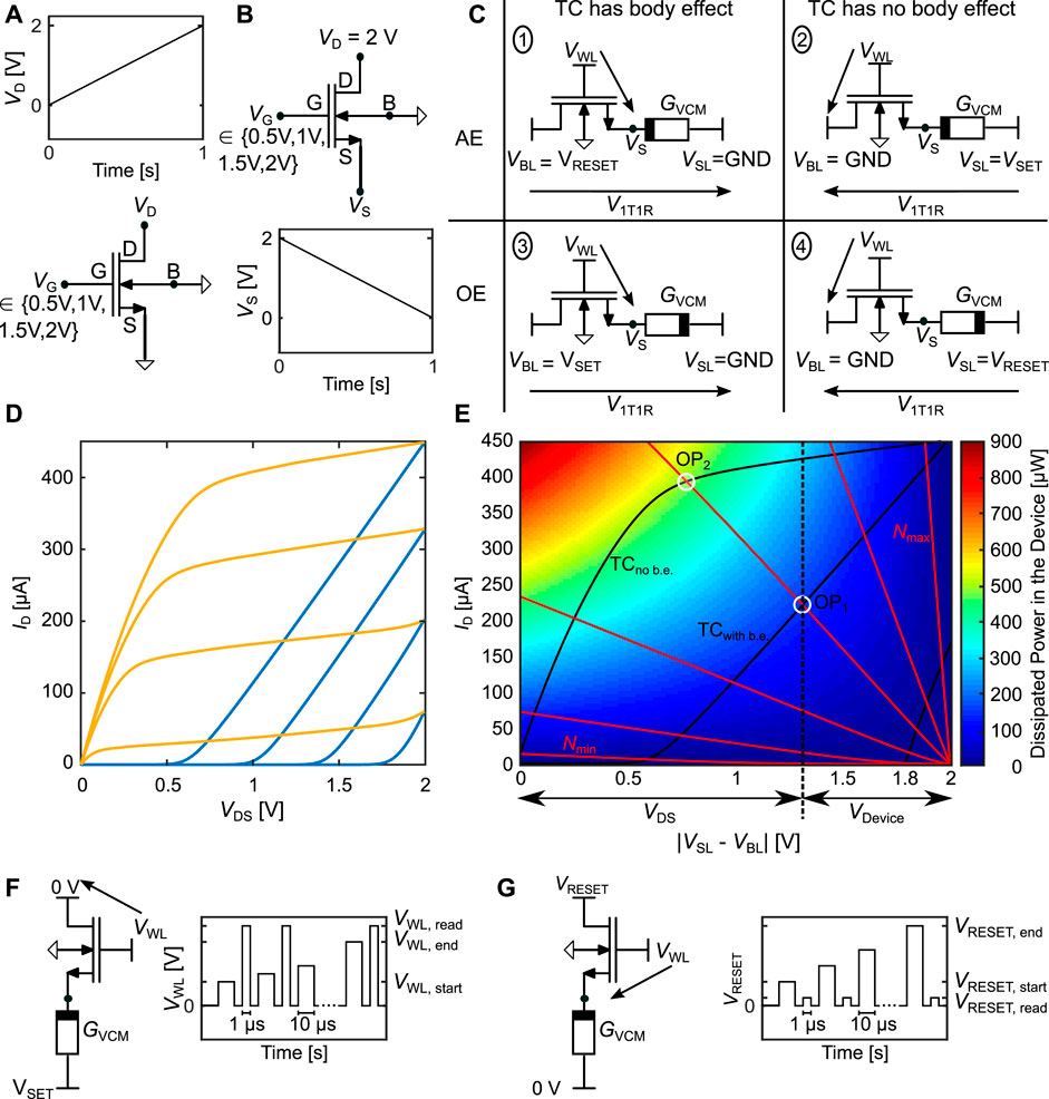
FIGURE 11. (A) shows the auxiliary circuit to simulate the transfer characteristic (TC) of the PTM 130 nm transistor model with the body effect (b.e.). (B) shows the schematic to simulate the TC with b. e. (C) shows the two possible configurations, AE or OE at transistor, of the 1T1R synapse. For each configuration the body effect has to be considered for one switching direction. (D) shows the TC of the simulated transistor (W = 260 nm L = 130 nm), with blue and without body effect yellow, at four different gate voltages (0.5 V, 1 V, 1.5 V and 2 V). (E) shows the adapted load line with the transistor from (D) at VG = 2 V (black lines), with and without body effect, and with the VCM cell at different states as load (red lines). The background is colored according to the power dissipated in the VCM device. (F) shows the typical way that the 1T1R synapse is operated in the potentiation direction, where VWL is increased over the pulse train, while VSET is kept constant. In the RESET direction we keep VWL constant while increasing VRESET as shown in (G).
In Figure 11E, we combine the TC with the VCM cells I-V-characteristic to gain a better understanding of the 1T1R behavior. The TCs with and without b. e. at VG = 2 V are displayed as solid black lines, the VCM cells I-V characteristic are added at different Ndisc values as the load (red lines). For this simulation, the ionic current was turned off to prevent switching of the cell. Due to the polarity dependent conduction mechanism of the VCM cell, one has to simulate the I-V characteristics for both polarities (Bengel et al. (2020)). Here, we only show the case of the SET direction. The RESET direction will be discussed in the following subsections. The background of Figure 11E is colored according to the power dissipated in the VCM device given through Pcell (I, V) = I ⋅ (Vdisc + Vplug + VSchottky), which is the same equation as for the RESET direction. The only difference between SET and RESET direction is the temperature change due to the dissipated power which is 20% smaller in the RESET case at the same power, due to the different thermal resistances. The dissipated power in the device is linearly proportional to the temperature change (Bengel et al. (2020)) and holds information about the temperature accelerated ionic movement of the oxygen vacancies in the disc. As the series resistance does not contribute to the Joule heating of the VCM device, it is excluded here and the power is reduced, when the series resistance starts to limit the switching. This temperature increase has been previously identified as the main force driving the non-linear switching kinetics (Menzel et al. (2011)). As the series resistance in this parameter set is in the order of 100 Ω (compare Supplementary Table S1) this only happens at very low resistances. The voltage on the x-axis refers to the voltage difference between SL and BL. For a certain operating point (e.g. OP1) the voltage dropping over the transistors Drain Source connection is given as the x-axis difference from origin to OP1. The voltage dropping over the VCM device is then the x-axis difference between OP1 and the applied voltage (here 2 V). Figure 11E shows two of the cases of Figure 11C, namely case 2 as the intersection points of the red lines with the TC without b. e. and case 3 as the intersection points of the red lines with the TC with b. e. The significance of the difference between these two cases can be understood from the difference between OP1 and OP2. In these two cases the VCM cell is in the same resistive state. While the current is larger by a factor of two in OP2, the dissipated power and thereby the induced temperature difference is even larger by a factor three. This leads to a faster and stronger SET switching. Another feature that can be inferred from the OP is the resilience against variability and noise in the transistor via the slope of the transistor characteristic in the OP. While the slope of the VCM cell is the same in both OPs, the transistor has a steeper slope in the OP1. This means, that the same voltage disturbance VDS will result in a stronger current disturbance, if the b. e. is present. We can thereby also increase the variability tolerance of the 1T1R synapse by increasing the Length of the transistor, as this reduces the TC slope in the saturation regime, while keeping
In the rest of this section we will investigate the SET and RESET behavior of the 1T1R synapse for the AE at the transistor and for the OE at the transistor. For this investigation, we perform potentiation and depression experiments over the course of 10 pulses, each of them 10 μs long, with the goal of achieving a gradual conductance tuning over the course of this pulse train. The conductances are chosen such that for each configuration the potentiation and depression can be concatenated if possible. This is achieved by aligning the conductance range after the potentiation with the conductance range before the depression and vice versa. For the AE configuration, we use a transistor sizing of W = 1,300 nm and L = 130 nm and for the OE configuration we use W = 390 nm and L = 130 nm.
We will first start with the AE configuration, where the body effect arises in the depression direction. Compared to Figure 11D the oxygen vacancy concentration now can change dynamically based on the equations of the model. Figures 12A, B show the load line analysis for the potentiation and depression direction, consisting of the transistor characteristic (grey from left to right), the device characteristic (white from right to left), the colored background indicating the power dissipated in the device and the various OPs (black circles). As the switching dynamics of the VCM cell do not only depend on the temperature acceleration, but also on the field acceleration (Menzel et al. (2011)), we also have to consider the strength of the electric field during potentiation and depression. Figures 12C, D shows the electric field driving the ionic movement for potentiation and depression as the background coloring, and the OPs as black circles. Additionally, showing the electric field helps in understanding the different contributions of the driving forces for the switching. As the electric field is calculated differently for the SET and RESET direction (Bengel et al. (2020)), the background color, which contains the magnitude of the electric field, of Figures 12C, D differs. For the SET direction, the electric field ESET used to calculate the ionic current depends only on the voltage dropping across the disc region. For an increasing cell voltage the electric field is always increased. Reducing the oxygen vacancy concentration increases the disc resistance. Depending on the oxygen vacancy concentration, different behaviors can be observed when the cell voltage is increased. Going to smaller oxygen vacancy concentrations increases the resistance of the disc which increases ESET. Going to even smaller oxygen vacancy concentrations, ESET reduces, as not only Rdisc increases, but also resistance of the Schottky diode. Towards very small oxygen vacancy concentration RSchottky increases faster than Rdisc, which reduces ESET. For the RESET direction, the relevant portion of the electric field also includes the voltage drops across the plug and the Schottky interface regions. In this case, only the electric field across the series resistance does not contribute to the ionic movement. This leads to the behavior that the electric field always increases for higher cell voltages and smaller vacancy concentrations in contrast to the SET direction. The simulations in Figures 12A-D are performed with the deterministic device parameter set. In Figures 12E, F the conductance evolution is shown for the deterministic parameter set and for ten devices with d2d and c2c variability.
FIGURE 12. Configuration AE for the potentiation (A, C, E) and depression (B, D, F) direction. (A, B) shows the load line analysis with the power dissipated in the device in the background. (C, D) show the development of the cell voltages at the different device states with the electric field driving the ionic motion in the background. (A, D) are using the deterministic model parameters. In (E, F) the deterministic conductance evolution (red diamonds) is shown together with ten runs exhibiting d2d and c2c variability (black circles).
In Figures 12A, C, E the characteristics of the potentiation are shown. Figure 12A shows the load line characteristics through the course of the potentiation experiment. In this experiment, we start with the VCM cell in the HRS state and apply ten pulses in the SET direction. Over the course of these pulses, we linearly increase the WL voltage from 0.4 V in the first pulse to 0.55 V in the last pulse. In this case, VGS is independent of the VCM device state, which means that the TC only changes due to the increase of the WL voltage. This changes the TC from lower currents at the first pulse to higher currents at the last pulse. The transistor is operated in the saturation regime, as the TC slope there is smaller compared to the linear regime, which gives a better robustness to variability as described above. The WL voltage range is quite small and well below the maximum possible voltages, due to the fact that we have a quite large transistor (W = 1,300 nm, L = 130 nm). This increase of the driving capability of the transistor is required to be able to RESET the VCM cell in the AE configuration, as will be shown later. For the chosen transistor sizing, the WL voltage range gives us the required range of saturation currents from around 50 μA at the first OP to around 270 μA at the last OP. The SET voltage applied at the BL is chosen very high at 2 V to prevent the VCM switching variability from affecting the behavior. Essentially, we want to have a high enough voltage to bring us into a regime, where the switching is only controlled and limited by the WL voltage controlling the transistor and not the VCM cells stochastic switching behavior. As the transistor changes to higher currents (due to the increasing WL voltage) and the VCM cell increases its conductance as it SETs, the OPs are moving towards higher amounts of dissipated power. The electric field during the potentiation (Figure 12C) increases for the first pulse and then continuously decreases over the remaining pulses. Therefore, we can say that as the SET progresses the influence of the heating for the switching process increases, while the influence of the electric field on the switching decreases. With the chosen parameters a very linear synapse dynamic can be achieved for all but the first pulses as shown in Figure 12E.
For the depression direction, load lines, field dependency and synaptic dynamics are shown in Figures 12B, D, F, respectively. Here, we start with the VCM cell in the LRS state and apply ten pulses in the RESET direction. The WL voltage is kept at 2.5 V at all times, to prevent a cutoff of the transistor which can occur if VGS drops below Vth as the VCM cell is too low conductive. Over the course of these pulses, we linearly increase the BL voltage from 1 V in the first pulse to 2 V in the last pulse. This can be described in the load line analysis as shifting the TC along the x-axis. The initial off phase of the transistor due to the body effect is then shifted to negative currents. The x-axis difference between the origin of the VCM characteristic and the intersection point of the TC with the x-axis is the actual voltage dropping over the 1T1R synapse. While the dissipated power increases from the first to the second pulse, this is due to the fact that the device is not switching yet, as the BL voltage is increased. As the device gets higher ohmic, the dissipated power decreases, as expected, which means that temperature acceleration of the ionic movement reduces. The first switching has to happen at a higher power, when compared to the first pulses in the potentiation direction, as the electric field is weaker by a factor of around seven. This factor drops to around three for the final pulses, but generally, the electric field is smaller in the depression direction than in the potentiation direction. The electric field is larger in the potentiation direction, as the main voltage drop is confined to a much shorter part of the switching layer. As the electric field increases while the power decreases, the influence of the electric field on the switching increases towards smaller LCS while the influence of the temperature decreases. With the chosen parameters, the switching is gradual and slow during the first pulses, then it becomes steeper and more linear before the slope is reduced again towards the end. It would be possible to start at a higher BL voltage to skip the initial slow changing phase, but, these higher BL voltages lead to a much more abrupt switching, in which almost the complete conductance range is traversed during the first few pulses.
To summarize, the AE configuration allows for a relatively gradual tuning with small variability in potentiation and depression direction. Both directions are also quite symmetrical except for the depression behavior at high conductances, however, this might be mitigated by reducing the dynamic range towards smaller maximum conductances. In this way, the symmetry (which in this case means linearity) can be traded of with the dynamic range, which has also been observed for the 1R synapse (section 3.1.1). As the initial and final conductances of potentiation and depression are compatible with each other, multiple cycles can be concatenated. In the next subsection, we want to focus on the 1T1R synapse, where the OE is connected to the transistor. The results are presented in an analogous fashion to the AE case in Figure 12.
Figure 13 depicts a potentiation and depression of the 1T1R synapse in the OE configuration for a transistor sizing of W = 390 nm and L = 130 nm. Here, the body effect arises for the potentiation direction. We again apply a pulse train consisting of ten pulses, each 10 μs long. For the potentiation (A, C and E) we hold the BL voltage at 2 V, while varying the WL voltage from 2 V during the first pulse to 2.2 V for the 10th pulse (A). The transistor is in the saturation regime throughout the complete operation. The increase in WL voltage shifts the TC towards higher currents allowing for higher HCS. As the TCs are relatively steep in the range of the operating points the cell voltage changes only over a small region (C). Again, the influence of the power on the switching increases towards higher conductances, while the influence of the electric field decreases. The resulting synaptic dynamics shown in Figure 13E shows a similar linearity to the AE configuration but with a much more pronounced variability. As described in section 5.1 this can be attributed to the slope of the TC in the vicinity of the OPs. The delay like regime occurs in the beginning, due to the insufficient voltage drop over the VCM cell.
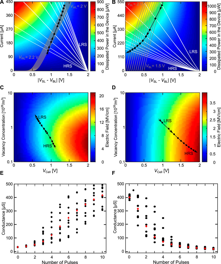
FIGURE 13. Configuration OE for the depression (A, C, E) and depression (B, D, F) direction. (A, B) shows the load line analysis for potentiation and depression direction, (C, D) show the development of the cell voltages driving the switching process. For (A, D) only the deterministic model parameters were used. In (E, F) the deterministic conductance evolution (red diamonds) is shown together with ten runs exhibiting d2d and c2c variability (black circles).
For the depression direction, Figures 13B, D, F, there is no body effect in the transistor, which allows for the operation of the VCM cell in the ohmic region or in the saturation region. A closer evaluation of both regimes shows, that a operation in the saturation regime would result in a more abrupt conductance change over the course of the depression. Once the voltage drop across the VCM cell is sufficient to trigger the RESET, the voltage divider will shift towards the VCM cell uncontrollably, thereby resulting in an abrupt decrease of the conductance. In contrast to that, when operating within the ohmic region, the transistor serves as a series resistance, which can adjust the voltage drop over the VCM device in a controlled manner and thus provides a more gradual RESET. We therefore operate the transistor solely in the linear region through the design of the
To summarize, the OE configuration allows for a relatively gradual and linear tuning with high variability towards the end of the pulse train in the potentiation direction. In the depression direction, the tuning is more abrupt, but also linear with large variability in the beginning, transitioning to a saturation behavior with small variability at the end of the pulse train. These behaviors of potentiation and depression are not very symmetrical. In analogy to the AE configuration, the symmetry could be improved by reducing the dynamic range towards higher minimum conductances. Again, the parameters where chosen such that potentiation and depression can be concatenated as the initial and final conductance values are compatible. Compared to the AE configuration, one advantage lies in the fact, that a smaller transistor can be used to operate the synapse. Another advantage is that it is easier to program very small LCS values since the transistor is not cut off.
In this work, different synapse concepts based on VCM ReRAM devices were investigated by using a physics-based compact model as well as experimental data on ZrOx based VCM devices. The synaptic dynamics were assessed under different performance metrics such as linearity, resolution, symmetry, dynamic range and variability tolerance. For a single VCM device, three regimes and thus three forms of synaptic dynamics were defined based on the specific device dynamics and physics, which are the delay, linear and saturation regime. As we have shown, those regimes are difficult to control or only allow for a limited analog performance. For the NR concept, we found, that either d2d or c2c variability is a requirement for the symmetry of the synapse and for achieving a gradually tuneable SET. Based on these results, we demonstrated the proposed concept of achieving different synaptic dynamics by choosing pulse amplitudes based on the switching probabilities and show, that we can achieve linear, symmetrical and reproducible synapse behavior. Those results are also verified experimentally. For the 1T1R concept, the effect of the connection direction between transistor and device on the switching behavior is explained through an adapted load line concept, which recognizes the impact of the different driving forces and includes the body effect of the transistor. For the AE configuration a good linearity and low variability can be achieved at the cost of relatively large transistors. In the OE configuration the synaptic dynamic is less linear and shows more variability. Comparing the different synapse concepts, it can be observed, that the 1R synapse provides the highest synapse density and easiest operation mode. However, it suffers from conductance fluctuations and a bad cyclability, due to the large impact of the d2d and c2c variability. In the NR concept, the inherent variability can be exploited, as long as the d2d variability is not too large, and allows for a good synapse operation. The 1T1R synapse in the AE configuration provides a very reliable and analog behavior at the expense of a large transistor. For the OE configuration, the variability is increased and the linearity decreased but smaller transistor sizings are possible as well as smaller LCS.
In this work, the operation of filamentary VCM based synapses is discussed for the case of pulse trains consisting of multiple rectangular pulses at constant voltage amplitude or at a changing amplitude. The conductance modulation is then associated with a specific singular pulse at a specific initial conductance. Additionally, we have mainly considered cases where the synapse is strongly potentiated or depressed at the beginning of the pulse train. For the investigation of the linear region of the 1R synapse, we have shown that addressing intermediate conductance ranges is associated with a small variability tolerance towards d2d and c2c variability of the VCM devices. In the context of neuromorphic learning rules, such as Spike-Timing-Dependent-Plasticity (STDP) (Kuzum et al. (2013)) and Spike Rate Dependent Plasticity (SRDP) (Xiong et al. (2019)) the timing of different spikes with respect to each other influences the conductance evolution. For STDP, the conductance of a synapse is adjusted based on the timing between a postsynaptic and a presynaptic spike. If the presynaptic spike precedes the postsynaptic spike, the synapse is potentiated and if the postsynaptic spike precedes the presynaptic spike, the synapse is depressed. For SRDP, spike trains are applied to the presynaptic neuron and the postsynaptic neuron with different frequencies. The conductance change is then a function of the relative frequencies of presynaptic and postsynaptic spike train to each other. Based on our results, it should be possible to optimize experiments and simulations of such biorealistic learning rules. The observed symmetry of STDP and SRDP will strongly depend on the considered conductance regime. Operating in the saturation and delay regime should deliver less symmetrical behavior for example. Generally, we have shown in this work that the dynamical behavior of a VCM device strongly depends on its conductance level before the application of the stimulus. This could prove a future optimization path for biorealistic learning rules by closely controlling their operating region.
In this paper, we have extensively investigated different synapse concepts based on VCM cells. This was done using experiments, but mainly through the use of our physics based compact model. Our work shows, that single VCM devices are strongly limited in their analog synaptic properties. This is mainly due to the d2d and c2c variability making the synapse behavior fundamentally difficult to control beyond an abrupt binary switching. We have discussed in detail the linear and saturation regime with regard to their quantitative behavior for a range of synapse evaluation criteria taken from literature. Using the NR synapse or the 1T1R synapse can be seen as different ways towards improving the properties of a single VCM devices for synapse applications. The idea behind using the NR synapse is that by averaging over the behavior of multiple devices, the non-ideal behavior of single devices has a smaller influence on the behavior of the whole synapse. For the NR synapse we started with identifying the impact and relevance of d2d and c2c variability on the synaptic dynamics. Additionally, we could show that different synaptic dynamics can be achieved via the exploitation of the switching percentages and through the use of changing pulse amplitudes. The idea behind the 1T1R synapse is to better control the behavior of the VCM devices through the transistor. For the 1T1R synapse we have analysed the difference between the two configurations in which the VCM cell can be connected to the transistor. If the AE is connected to the transistor the behavior is generally more favourable with a linear tuning across a large range of conductances and a smaller observed variability. However, the AE configuration requires larger transistors for the RESET direction. Design trade offs and limitations are introduced and discussed through the introduction of an adapted load line concept, which takes into account the power dissipation in the device as well as by taking into account the electric field driving the ionic motion during switching. Those two quantities represent the driving forces governing the VCM behavior. For all observed synapse concepts, a clear trade off between the dynamic range and the linearity can be observed.
The raw data supporting the conclusion of this article will be made available by the authors, without undue reservation.
CB and KZ performed the modeling and simulation. JM conducted the experiments. TZ contributed to the theory. SW fabricated the devices. CB, KZ, and JM wrote the manuscript. DW, RW, and SM performed the review, editing and supervision. All authors listed have made a substantial, direct and intellectual contribution to the work, and approved it for publication.
This work was in part funded by the German Research Foundation (DFG) under Grant No. SFB 917, in part by the Federal Ministry of Education and Research (BMBF, Germany) in the project NEUROTEC II (Project Nos. 16ME0398K and 16ME0399), in part by the European Union’s Horizon 2020 Research and Innovation Program through the project MNEMOSENE under Grant No. 780215, in part by the Helmholtz Association Initiative and Networking Fund (Advanced Computing Architectures (ACA)) under Project SO- 092, and it is based on the Jülich Aachen Research Alliance (JARA-FIT).
The authors declare that the research was conducted in the absence of any commercial or financial relationships that could be construed as a potential conflict of interest.
All claims expressed in this article are solely those of the authors and do not necessarily represent those of their affiliated organizations, or those of the publisher, the editors and the reviewers. Any product that may be evaluated in this article, or claim that may be made by its manufacturer, is not guaranteed or endorsed by the publisher.
The Supplementary Material for this article can be found online at: https://www.frontiersin.org/articles/10.3389/femat.2023.1061269/full#supplementary-material
Ascoli, A., Menzel, S., Rana, V., Kempen, T., Messaris, I., Demirkol, A. S., et al. (2022). A deep study of resistance switching phenomena in TaOx reram cells: System-theoretic dynamic route map analysis and experimental verification. Adv. Electron. Mater. 8, 2200182. doi:10.1002/aelm.202200182
Ascoli, A., Tetzlaff, R., and Menzel, S. (2018). Exploring the dynamics of real-world memristors on the basis of circuit theoretic model predictions. IEEE Circuits Syst. Mag. 18, 48–76. doi:10.1109/MCAS.2018.2821760
Bengel, C., Cüppers, F., Payvand, M., Dittmann, R., Waser, R., Hoffmann-Eifert, S., et al. (2021a). Utilizing the switching stochasticity of HfO2/TiOx-based ReRAM devices and the concept of multiple device synapses for the classification of overlapping and noisy patterns. Front. Neurosci. 15, 661856. doi:10.3389/fnins.2021.661856
Bengel, C., and Menzel, S. (2019). JART VCM v1b var. Available at: http://www.emrl.de/JART.html (accessed September 12, 2022).
Bengel, C., Mohr, J., Wiefels, S., Singh, A., Gebregiorgis, A., Bishnoi, R., et al. (2022). Reliability aspects of binary vector-matrix-multiplications using ReRAM devices. Neuromorphic Comput. Eng. 2, 034001. doi:10.1088/2634-4386/ac6d04
Bengel, C., Siemon, A., Cüppers, F., Hoffmann-Eifer, S., Hardtdegen, A., von Witzleben, M., et al. (2020). “Variability-aware modeling of filamentary oxide based bipolar resistive switching cells using SPICE level compact models,” in IEEE Transactions on Circuits and Systems I: Regular Papers (IEEE). doi:10.1109/TCSI.2020.3018502
Bengel, C., Siemon, A., Rana, V., and Menzel, S. (2021b). “Implementation of multinary lukasiewicz logic using memristive devices,” in 2021 IEEE International Symposium on Circuits and Systems (ISCAS), Daegu, Korea, 22-28 May, 2021.
Boybat, I., Gallo, M. L., Nandakumar, S. R., Moraitis, T., Parnell, T., Tuma, T., et al. (2018a). Neuromorphic computing with multi-memristive synapses. Nat. Commun. 9, 2514. doi:10.1038/s41467-018-04933-y
Boybat, I., Gallo, M. L., Nandakumar, S. R., Moraitis, T., Parnell, T., Tuma, T., et al. (2018b). Neuromorphic computing with multi-memristive synapses. Nat. Commun. 9. doi:10.1038/s41467-018-04933-y
Brivio, S., Ly, D. R. B., Vianello, E., and Spiga, S. (2021). Non-linear memristive synaptic dynamics for efficient unsupervised learning in spiking neural networks. Front. Neurosci. 15, 580909. doi:10.3389/fnins.2021.580909
Burr, G. W., Shelby, R. M., Sebastian, A., Kim, S., Kim, S., Sidler, S., et al. (2017). Neuromorphic computing using non-volatile memory. Adv. Phys.-X 2, 89–124. doi:10.1080/23746149.2016.1259585
Christensen, D. V., Dittmann, R., Linares-Barranco, B., Sebastian, A., Gallo, M. L., Redaelli, A., et al. (2022). 2022 roadmap on neuromorphic computing and engineering. Neuromorphic Comput. Eng. 2, 022501. doi:10.1088/2634-4386/ac4a83
Chua, L. (2018). Five non-volatile memristor enigmas solved. Appl. Phys. A 124, 563. doi:10.1007/s00339-018-1971-0
Chua, L., and Kang, S. (1976). Memristive devices and systems. Proc. IEEE 64, 209–223. doi:10.1109/proc.1976.10092
Covi, E., Brivio, S., Serb, A., Prodromakis, T., Fanciulli, M., and Spiga, S. (2016). Analog memristive synapse in spiking networks implementing unsupervised learning. Front. Neurosci. 10, 482. doi:10.3389/fnins.2016.00482
Cüppers, F., Menzel, S., Bengel, C., Hardtdegen, A., von Witzleben, M., Böttger, U., et al. (2019). Exploiting the switching dynamics of HfO2-based ReRAM devices for reliable analog memristive behavior. Apl. Mater. 7, 091105. doi:10.1063/1.5108654
Dalgaty, T., Payvand, M., Moro, F., Ly, D. R. B., Pebay-Peyroula, F., Casas, J., et al. (2019). Hybrid neuromorphic circuits exploiting non-conventional properties of RRAM for massively parallel local plasticity mechanisms. Apl. Mater. 7, 081125. doi:10.1063/1.5108663
DiCiccio, T. J., and Efron, B. (1996). Bootstrap confidence intervals. Stat. Sci. 11, 189–212. doi:10.1214/ss/1032280214
Dittmann, R., Menzel, S., and Waser, R. (2022). Nanoionic memristive phenomena in metal oxides: The valence change mechanism. Adv. Phys. 71, 155–349. doi:10.1080/00018732.2022.2084006
Fleck, K., Torre, C. L., Aslam, N., Hoffmann-Eifert, S., Böttger, U., and Menzel, S. (2016). Uniting gradual and abrupt SET processes in resistive switching oxides. Phys. Rev. Appl. 6, 064015. doi:10.1103/physrevapplied.6.064015
Fouda, M. E., Kurdahi, F., Eltawil, A., and Neftci, E. (2020). “Chapter 19 - Spiking Neural Networks for inference and learning: A memristor-based design perspective,” in Memristive devices for brain-inspired computing. Editors S. Spiga, A. Sebastian, D. Querlioz, and B. Rajendran (Duxford: Woodhead Publishing Woodhead Publishing Series in Electronic and Optical Materials), 499–530. doi:10.1016/B978-0-08-102782-0.00019-8
Frascaroli, J., Brivio, S., Covi, E., and Spiga, S. (2018). Evidence of soft bound behaviour in analogue memristive devices for neuromorphic computing. Sci. Rep. 8. doi:10.1038/s41598-018-25376-x
Fusi, S., and Abbott, L. F. (2007). Limits on the memory storage capacity of bounded synapses. Nat. Neurosci. 10, 485–493. doi:10.1038/nn1859
Gaba, S., Sheridan, P., Zhou, J., Choi, S., and Lu, W. (2013). Stochastic memristive devices for computing and neuromorphic applications. Nanoscale 5, 5872–5878. doi:10.1039/c3nr01176c
Garbin, D., Vianello, E., Bichler, O., Rafhay, Q., Gamrat, C., Ghibaudo, G., et al. (2015). HfO2-Based OxRAM Devices as Synapses for Convolutional Neural Networks. HfO2-based OxRAM devices as synapses convolutional neural Netw. 62, 2494–2501. doi:10.1109/ted.2015.2440102
Gokmen, T., and Haensch, W. (2020). Algorithm for training neural networks on resistive device arrays. Front. Neurosci. 14, 103. doi:10.3389/fnins.2020.00103
Govoreanu, B., Kar, G., Chen, Y.-Y., Paraschiv, V., Kubicek, S., Fantini, A., et al. (2011). “10×10nm2 Hf/HfOX crossbar resistive RAM with excellent performance, reliability and low-energy operation,” in 2011 International Electron Devices Meeting (IEEE).
Ham, D., Park, H., Hwang, S., and Kim, K. (2021). Neuromorphic electronics based on copying and pasting the brain. Nat. Electron. 4, 635–644. doi:10.1038/s41928-021-00646-1
Hardtdegen, A., La Torre, C., Zhang, H., Funck, C., Menzel, S., Waser, R., et al. (2016). “Internal cell resistance as the origin of abrupt RESET behavior in HfO2-based devices determined from current compliance series,” in 2016 IEEE 8th International Memory Workshop (New York: IMW), 1–4. doi:10.1109/IMW.2016.7495280
Hardtdegen, A., Torre, C. L., Cuppers, F., Menzel, S., Waser, R., and Hoffmann-Eifert, S. (2018). Improved switching stability and the effect of an internal series resistor in HfO2/TiOX bilayer ReRAM cells. IEEE Trans. Electron Devices 65, 3229–3236. doi:10.1109/ted.2018.2849872
Jung, S., Lee, H., Myung, S., Kim, H., Yoon, S. K., Kwon, S., et al. (2022). A crossbar array of magnetoresistive memory devices for in-memory computing. Nature 601, 211–216. doi:10.1038/s41586-021-04196-6
Kim, T., Hu, S., Kim, J., Kwak, J. Y., Park, J., Lee, S., et al. (2021). Spiking neural network (SNN) with memristor synapses having non-linear weight update. Front. Comput. Neurosci. 15, 646125. doi:10.3389/fncom.2021.646125
Kuzum, D., Yu, S., and Wong, H.-S. P. (2013). Synaptic electronics: Materials, devices and applications. Nanotechnology 24, 382001. doi:10.1088/0957-4484/24/38/382001
Li, J., Luan, B., and Lam, C. (2012). “Resistance drift in phase change memory,” in 2012 IEEE International Reliability Physics Symposium (IRPS), 1–6.6C
Maldonado, D., Gonzalez, M. B., Campabadal, F., Jimenez-Molinos, F., Chawa, M. M. A., Stavrinides, S. G., et al. (2020). Experimental evaluation of the dynamic route map in the reset transition of memristive ReRAMs. ReRAMs 139, 110288. doi:10.1016/j.chaos.2020.110288
Marrone, F., Secco, J., Kersting, B., Le Gallo, M., Corinto, F., Sebastian, A., et al. (2022). Experimental validation of state equations and dynamic route maps for phase change memristive devices. Sci. Rep. 6488. doi:10.1038/s41598-022-09948-6
Mead, C., and Ismail, M. (1989). “Analog VLSI implementation of neural systems,” in The springer international series in engineering and computer science (Boston, MA: Springer). doi:10.1007/978-1-4613-1639-8
Mehonic, A., Sebastian, A., Rajendran, B., Simeone, O., Vasilaki, E., and Kenyon, A. J. (2020). Memristors-from in-memory computing, deep learning acceleration, and spiking neural networks to the future of neuromorphic and bio-inspired computing. Hoboken: Wiley, 2000085.
Menzel, S., von Witzleben, M., Havel, V., and Böttger, U. (2019). The ultimate switching speed limit of redox-based resistive switching devices. Faraday Discuss. 213, 197–213. doi:10.1039/C8FD00117K
Menzel, S., Waters, M., Marchewka, A., Böttger, U., Dittmann, R., and Waser, R. (2011). Origin of the ultra-nonlinear switching kinetics in oxide-based resistive switches. Adv. Funct. Mater. 21, 4487–4492. doi:10.1002/adfm.201101117
Milo, V., Glukhov, A., Pérez, E., Zambelli, C., Lepri, N., Mahadevaiah, M. K., et al. (2021). Accurate program/verify schemes of resistive switching memory (RRAM) for in-memory neural network circuits. IEEE Trans. Electron Devices 68, 3832–3837. doi:10.1109/ted.2021.3089995
Moon, K., Lim, S., Park, J., Sung, C., Oh, S., Woo, J., et al. (2019). RRAM-based synapse devices for neuromorphic systems. Faraday Discuss. 213, 421–451. doi:10.1039/c8fd00127h
Nanoscale Integration and Modeling (NIMO) Group at ASU (2006). 130nm BSIM4 model card for bulk CMOS. Available at: http://ptm.asu.edu/modelcard/2006/130nm_bulk.pm (accessed 01 April, 2021).
Park, S., Kim, H., Choo, M., Noh, J., Sheri, A., Jung, S., et al. (2012). “RRAM-based synapse for neuromorphic system with pattern recognition function,” in 2012 IEEE International Electron Devices Meeting (IEDM) (2012 IEEE International Electron Devices Meeting (New York: IEDM), 1021–1024.
Singha, A., Muralidharan, B., and Rajendran, B. (2014). “Analog memristive time dependent learning using discrete nanoscale RRAM devices,” in 2014 International Joint Conference on Neural Networks (IJCNN), 2248–2255.
Stathopoulos, S., Khiat, A., Cortese, M. T. S., Serb, A., Valov, I., Prodromakis, T., et al. (2017). Multibit memory operation of metal-oxide bi-layer memristors. Sci. Rep. 7, 17532. doi:10.1038/s41598-017-17785-1
Strachan, J. P., Torrezan, A. C., Miao, F., Pickett, M. D., Yang, J. J., Yi, W., et al. (2013). State dynamics and modeling of tantalum oxide memristors. IEEE Trans. Electron Devices 60, 2194–2202. doi:10.1109/ted.2013.2264476
Strukov, D. B., Snider, G. S., Stewart, D. R., and Williams, R. S. (2008). The missing memristor found. Nature 453, 80–83. doi:10.1038/nature06932
Sung, C., Hwang, H., and Yoo, I. K. (2018). Perspective: A review on memristive hardware for neuromorphic computation. J. Appl. Phys. 124, 151903. doi:10.1063/1.5037835
Vaccaro, F., Brivio, S., Perotto, S., Mauri, A. G., and Spiga, S. (2022). Physics-based compact modelling of the analog dynamics of HfO x resistive memories. Neuromorphic Comput. Eng. 2, 021003. doi:10.1088/2634-4386/ac7327
von Witzleben, M., Walfort, S., Waser, R., Menzel, S., and Böttger, U. (2021a). Determining the electrical charging speed limit of ReRAM devices. IEEE J. Electron Devices Soc. 9, 667–678. doi:10.1109/JEDS.2021.3095389
von Witzleben, M., Wiefels, S., Kindsmüller, A., Stasner, P., Berg, F., Cüppers, F., et al. (2021b). Intrinsic RESET speed limit of Valence Change Memories. ACS Appl. Electron. Mat. 3, 5563–5572. doi:10.1021/acsaelm.1c00981
Waser, R., and Aono, M. (2007). Nanoionics-based resistive switching memories. Nat. Mat. 6, 833–840. doi:10.1038/nmat2023
Waser, R., Dittmann, R., Staikov, G., and Szot, K. (2009). Redox-based resistive switching memories - nanoionic mechanisms, prospects, and challenges. Adv. Mater. 21, 2632–2663. doi:10.1002/adma.200900375
Waser, R., Ielmini, D., Akinaga, H., Shima, H., Wong, H.-S. P., Yang, J. J., et al. (2016). “Introduction to nanoionic elements for information technology,” in Resistive switching (Wiley-VCH Verlag GmbH and Co. KGaA), 1–30. doi:10.1002/9783527680870.ch1
Wiefels, S., Bengel, C., Kopperberg, N., Zhang, K., Waser, R., and Menzel, S. (2020). “HRS instability in oxide based bipolar resistive switching cells,” in IEEE Transactions on Electron Devices. doi:10.1109/TED.2020.3018096
Xia, Q., and Yang, J. J. (2019). Memristive crossbar arrays for brain-inspired computing. Nat. Mater. 18, 309–323. doi:10.1038/s41563-019-0291-x
Xiong, J., Yang, R., Shaibo, J., Huang, H. M., He, H. K., Zhou, W., et al. (2019). Bienenstock, cooper, and munro learning rules realized in second-order memristors with tunable forgetting rate. Adv. Funct. Mater. 29, 1807316. doi:10.1002/adfm.201807316
Xue, C.-X., Huang, T.-Y., Liu, J.-S., Chang, T.-W., Kao, H.-Y., Wang, J.-H., et al. (2020). “A 22nm 2mb ReRAM compute-in-memory macro with 121-28tops/w for multibit mac computing for tiny ai edge devices,” in 2020 IEEE International Solid- State Circuits Conference - (ISSCC), 244–246.
Yang, J., Zhu, J., Dang, B., Zhang, T., Duan, Q., Xu, L., et al. (2020). “TaOx synapse array based on ion profile engineering for high accuracy neuromorpic computing,” in 2020 China Semiconductor Technology International Conference (CSTIC), 1–4.
Yao, P., Wu, H., Gao, B., Tang, J., Zhang, Q., Zhang, W., et al. (2020). Fully hardware-implemented memristor convolutional neural network. Nature 577, 641–646. doi:10.1038/s41586-020-1942-4
Zahari, F., Pérez, E., Mahadevaiah, M. K., Kohlstedt, H., Wenger, C., and Ziegler, M. (2020). Analogue pattern recognition with stochastic switching binary CMOS-integrated memristive devices. Sci. Rep. 10, 14450. doi:10.1038/s41598-020-71334-x
Zhao, M., Gao, B., Tang, J., Qian, H., and Wu, H. (2020). Reliability of analog resistive switching memory for neuromorphic computing. API 7, 011301. doi:10.1063/1.5124915
Zidan, M. A., Fahmy, H. A. H., Hussain, M. M., and Salama, K. N. (2013). Memristor-based memory: The sneak paths problem and solutions. Microelectron. J. 44, 176–183. doi:10.1016/j.mejo.2012.10.001
Keywords: neuromorphic computing, ReRAM, artificial synapse, memristor, artificial neural network
Citation: Bengel C, Zhang K, Mohr J, Ziegler T, Wiefels S, Waser R, Wouters D and Menzel S (2023) Tailor-made synaptic dynamics based on memristive devices. Front. Electron. Mater. 3:1061269. doi: 10.3389/femat.2023.1061269
Received: 04 October 2022; Accepted: 16 January 2023;
Published: 26 January 2023.
Edited by:
Yao Shuai, University of Electronic Science and Technology of China, ChinaReviewed by:
Rivu Midya, Massachusetts Institute of Technology, United StatesCopyright © 2023 Bengel, Zhang, Mohr, Ziegler, Wiefels, Waser, Wouters and Menzel. This is an open-access article distributed under the terms of the Creative Commons Attribution License (CC BY). The use, distribution or reproduction in other forums is permitted, provided the original author(s) and the copyright owner(s) are credited and that the original publication in this journal is cited, in accordance with accepted academic practice. No use, distribution or reproduction is permitted which does not comply with these terms.
*Correspondence: Christopher Bengel, Y2hyaXN0b3BoZXIuYmVuZ2VsQHJ3dGgtYWFjaGVuLmRl; Stephan Menzel, c3QubWVuemVsQGZ6LWp1ZWxpY2guZGU=
†These authors have contributed equally to this work
Disclaimer: All claims expressed in this article are solely those of the authors and do not necessarily represent those of their affiliated organizations, or those of the publisher, the editors and the reviewers. Any product that may be evaluated in this article or claim that may be made by its manufacturer is not guaranteed or endorsed by the publisher.
Research integrity at Frontiers
Learn more about the work of our research integrity team to safeguard the quality of each article we publish.