- The 50th Research Institute of China Electronics Technology Group Corporation, Shanghai, China
Terahertz (THz) Si-based blocked-impurity-band (BIB) detector is becoming the overwhelming choice for applications in space-based instruments, airborne, and imaging systems. A high-performance linear scan imaging system based on the THz Si-based BIB detector is designed. Through the optimized design of cryogenic Dewar and a suitable optical system, the imaging system reduces background stray radiation, and then improves the THz imaging performance of the detector. At the temperature of 4.2 K and the bias of 2.6V, the blackbody peak responsivity of the Si-based BIB detector is 23.77A/W, while the dark current is
1 Introduction
The wave band of terahertz (THz) waves (range from 0.1 to 10 THz) is between microwave and infrared, so it combines many characteristics of microwave and infrared (Ferguson and Zhang, 2002). The blocked-impurity-band (BIB) detector is a new type of THz detector, which uses low-frequency breakthrough technology from infrared to achieve THz detection. With its high sensitivity, large array scale, and wide detection spectrum advantages (Iglesias et al., 2008; Woods et al., 2011), the BIB detector stands out among the THz detectors and has been widely used in space target detection (Reynolds et al., 1989; Werner, 2005), atmospheric monitoring (Hogue et al., 2008), astronomical observation (Hanaoka et al., 2016; Xiao et al., 2022) and other fields (Kaplan et al., 2021; Meng et al., 2022).
Imaging technology for THz waves is an important direction of THz research (Jepsen et al., 2010; Kanda et al., 2017; Guerboukha et al., 2018; Chapdelaine et al., 2022). Compared to microwaves, THz imaging offers superior spatial resolution due to its shorter wavelength (Baxter and Guglietta, 2011; Hübers et al., 2013). Compared with infrared, THz imaging has a higher temperature resolution when detecting low-temperature targets due to its longer wavelength (according to Wien displacement law). In the cryogenic environment (≤6 K), the dark current of the BIB detector will be better suppressed, and the signal-to-noise ratio of the BIB detector will be greatly improved (Liao et al., 2014; Wang et al., 2018; Wang et al., 2019). Therefore, the BIB detector is more conducive to the detection of weak radiation targets.
This work introduces the BIB detector and establishes a high-performance linear scan imaging system. Through the optimized design of cryogenic Dewar and a suitable optical system, the background stray radiation of the imaging system is reduced and the THz imaging performance of the detector is improved. The system realizes the real-time imaging of room-temperature objects and shows an overwhelming advantage over single-pixel point-by-point imaging system in the time dimension. The results indicate that the BIB detector has a clear resolution on the room or low temperature objects detecting.
2 Experimental
2.1 Setup of the THz linear scan imaging system
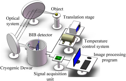
The diagram of the whole system is shown in Figure 1.The temperature control system keeps the cryogenic Dewar in a cryogenic environment suitable for the detector operation, and the object is placed on a two-dimensional translation stage. The radiation generated by the object is reflected by two off-axis parabolic mirrors and reaches the Si-based BIB detector in the cryogenic Dewar. The detector generates a tiny current signal after absorbing the radiation, and then the current signal is transmitted to the signal acquisition unit through the transmission line in the cryogenic Dewar. The signal acquisition unit amplifies and converts the tiny current signal from the detector into a voltage signal that can be collected and quantified by the ADC (Analog to Digital Converter) module. The collected data is transmitted to the image processing program through the Ethernet, and is displayed on the screen in real-time after image processing.
2.2 THz Si-based BIB detector
The diagram of Si-based BIB detector is shown in Figure 2A, including high-conductivity Si substrate, absorption layer, blocking layer, passivation layer, anode and cathode formed by mesa etching and metal deposition. Si-based BIB detectors use epitaxial growth technology to deposit a heavily doped absorption layer and a high-purity intrinsic blocking layer on the high-conductivity substrate to form a BIB structure.
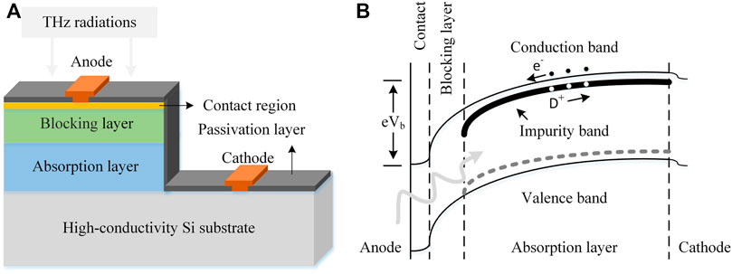
FIGURE 2. (A) The diagram of Si-based BIB detector. (B) The band gap structure of silicon-based BIB detector.
The heavily doped elements (P) of the absorption layer form an impurity band between the conduction and valence bands, as shown in Figure 2B. When the THz radiation is irradiated on the detector and absorbed by the absorption layer, the generated electrons will transition from the impurity band to the conduction band, and the electrons after the transition are collected by the positive electrode through the curved conduction band, thereby realizing the transformation of the detector signal from an optical signal to electrical signal.
The BIB detector uses the heavily doped absorption layer to absorb THz radiation, and uses the intrinsic blocking layer to suppress the dark current and noise of the device. This design makes the BIB detector a high-speed, high-sensitivity and wide-spectrum THz detector.
The characteristics of the Si-based BIB detector used in this work are shown in Figure 3.
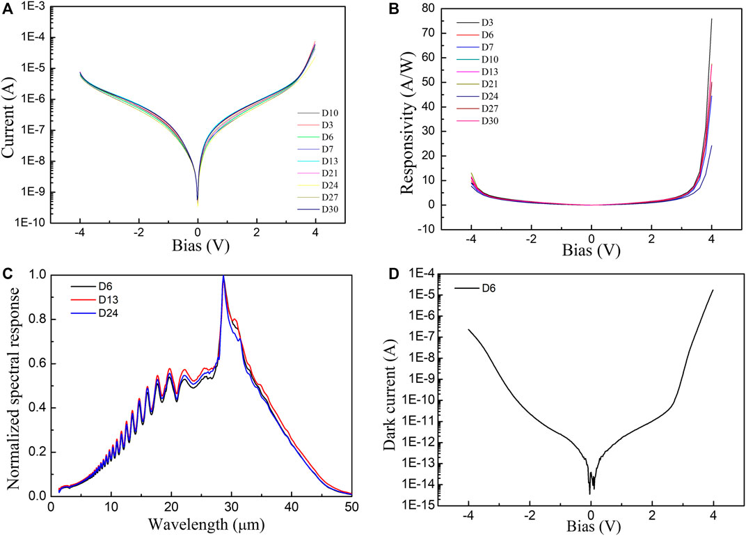
FIGURE 3. (A) The I-V curve of Si-based BIB detector different pixels under different biases. (B) The responsivity of the Si-based BIB detector different pixels under different biases. (C) The spectral responsivity of Si-based BIB detector measured by Fourier Transform Infrared Spectrometer (D) The dark current of the Si-based BIB detector under different biases.
The results are measured at the cryogenic environment (4.2 K) and the chopper frequency is 35.97 Hz. The responsivity of the Si-based BIB detector is expressed as (Tao et al., 2021)
where Ipc is the response current value, t (0.7) is the transmittance of cryogenic Dewar filter, σ is the Stepan-Boltzmann constant, L (10 cm) is the distance between the device and the blackbody. Ab (0.01 mm2), Ad (0.01 mm2), T1 (300K), and T2 (800K) represent the blackbody radiation area, pixel area, room temperature and blackbody temperature, respectively.
The responsivity non-uniformity is expressed as (Yin et al., 2020).
Where M is the total number of pixels, d is the number of death pixels,
Different pixels are tested to study the non-uniformity of Si-based BIB detector. Figures 3A, B shows the responsivity of the detector is around 2.22 A/W and the responsivity non-uniformity is less than 6.8% when the bias is 2.6 V.
Due to the good responsivity uniformity of detector pixels, this work randomly selects a pixel (D6) for further testing. Figure 3C shows that the spectral responsivity range of the detector is
The blackbody peak responsivity
Where
The blackbody peak responsivity of the Si-based BIB detector is 23.77A/W. Figure 3D shows the dark current of the detector is
2.3 Cryogenic dewar
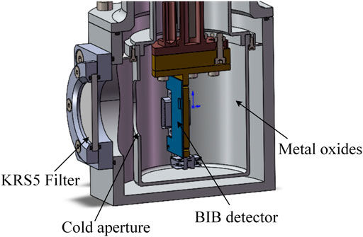
Background stray radiation is an important factor limiting the performance of the device. Reducing the background stray radiation can effectively improve the signal-to-noise ratio (SNR) of the device and the performance of the detector. In order to verify the imaging effect of the Si-based BIB detector in the THz band, we optimized the design of the cryogenic Dewar. The structure of the cryogenic Dewar is shown in Figure 4.
To avoid the influence of visible light, a KRS5 filter is installed on the Dewar window, which has 70% transmittance in the spectral range of 500 nm to 35 µm. However, the KRS5 filter is placed at room-temperature and is facing the detector, so the stray radiation emitted by itself has a great influence on the background noise of the detector. In addition, since the detector is placed directly in the Dewar, the stray radiation emitted by the inner wall of the Dewar will also affect the background noise of the detector.
In order to solve the influence of stray radiation, another low-pass filter is added outside the cold aperture to filter the radiation from the KRS5. In addition, the conical surface of the inner wall of the cold aperture and the inner wall surface of the connecting cylinder are designed to cover with metal oxides with high absorption and high ignition point. This design can achieve more than two absorption reflections, effectively attenuate the stray radiation energy to the detection surface and improve the SNR of the detector.
2.4 Optical system
The optical system is mainly composed of two off-axis parabolic mirrors, two-dimensional translation stage, object and Si-based BIB detector.
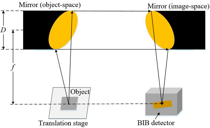
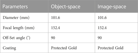
In order to improve the energy of the light signal received by the detector, off-axis parabolic mirrors are used to realize the light path convergence in this work. The surface of the mirrors has a gold coating to minimize the scattering loss in the light focusing application. The reflectivity in the Si-based BIB detector band can reach 99%. And it has the advantages of simple structure, easy processing, adjustment and high spatial resolution. Figure 5 shows the diagram of the optical imaging system. The specifications of two off-axis parabolic mirrors are shown in Table 1.
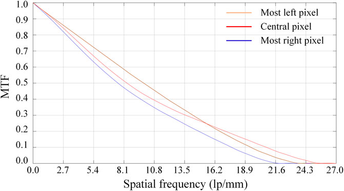
The modulation transfer function (MTF) expresses the relationship between the degree of modulation and the number of line pairs per millimeter within the image, and is the most comprehensive criterion for judging the performance of any optical system, especially for imaging systems. The MTF is usually given as a plot of amplitude response versus frequency in cycles per millimeter. The spatial resolution of the imaging system can be obtained from the MTF diagram. In this work, the linear Si-based BIB detector is used, and the MTF of the center pixel and the edge pixels are studied through ZEMAX simulation.
Figure 6 shows the MTF curves of pixels at different positions of the linear Si-based BIB detector. It can be seen that the spatial cutoff frequency of the imaging system is about 21.6lp/mm, indicating that the optical system can produce 21.6 pairs of line pairs with the same size in the range of 1 mm. So the spatial resolution of the optical system is
3 Results
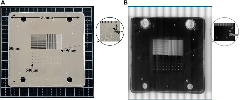
The object imaging verification uses a metal resolution plate for imaging at room temperature. The metal resolution plate has metal hollows designed according to specifications, which can be used to observe the resolution of the imaging system.
The temperature variations on the surface of the metal plate in Figure 7A are less than 2 K. The size of the metal resolution plate is 50 mm × 50 mm, and there are five rows of 10 small holes on the plate, increasing at intervals of 10 µm from right to left. The minimum aperture is 50 µm and the maximum aperture is 540 µm. The fine stripe structures of the metal plate vary from 50 µm to 300 μm, distributed both vertically and horizontally. The details and textures on the plate are clearly visible in the imaging results (Figure 7B), indicating the good imaging capability of the imaging system. The blackbody is placed at the focal point of the object-space mirror, and the NTED of the entire system is about 10 mK by calibrating the blackbody at different temperatures.
4 Discussion
Based on the THz Si-based BIB detector, a high-performance linear scan imaging system is designed. The experimental results show that the NETD of the whole system reaches 10 mK, and the spatial resolution reaches 50 µm. Image overlap is due to the use of open-loop control of the stepper motor and its impact can be eliminated by using closed-loop control or changing the motor type. This work is beneficial to the further research of Si-based BIB detectors in the fields of space target detection and astronomical observation.
Data availability statement
The original contributions presented in the study are included in the article/Supplementary Material, further inquiries can be directed to the corresponding authors.
Author contributions
XW: resources and funding acquisition. JW, CZ, and HZ: system design. LZ: Software. DC: Detector testing. JW and CZ: experiment and original draft preparation. JW, JJ-T, and XW: Review the manuscript. All authors contributed to the article and agreed to the published version of the manuscript.
Funding
The authors gratefully acknowledge the support by the National Natural Science Foundation of China (No. 62171286) and Program of Shanghai Academic/Technology Research Leader (Grant No. 21XD1423600). This work is also supported by the Shanghai Sailing Program (Grant No. 22YF1446200).
Conflict of interest
JW, JJ-T, CZ, HZ, LZ, DC, and XW were employed by The 50th Research Institute of China Electronics Technology Group Corporation.
Publisher’s note
All claims expressed in this article are solely those of the authors and do not necessarily represent those of their affiliated organizations, or those of the publisher, the editors and the reviewers. Any product that may be evaluated in this article, or claim that may be made by its manufacturer, is not guaranteed or endorsed by the publisher.
References
Baxter, J. B., and Guglietta, G. W. (2011). Terahertz spectroscopy. Anal. Chem. 83 (12), 4342–4368. doi:10.1021/ac200907z
Ferguson, B., and Zhang, X.-C. (2002). Materials for terahertz science and technology. Nat. Mater. 1 (1), 26–33. doi:10.1038/nmat708
Guerboukha, H., Nallappan, K., and Skorobogatiy, M. (2018). Toward real-time terahertz imaging. Adv. Opt. Photonics 10 (4), 843. doi:10.1364/aop.10.000843
Hogue, H. H., Mlynczak, M. G., Abedin, M. N., Masterjohn, S. A., and Huffman, J. E. (2008). Far-infrared detector development for space-based Earth observation. SPIE Proc. doi:10.1117/12.797078
Hübers, H.-W., Eichholz, R., Pavlov, S. G., and Richter, H. (2013). High resolution terahertz spectroscopy with quantum cascade lasers. J. Infrared, Millim. Terahertz Waves 34 (5-6), 325–341. doi:10.1007/s10762-013-9973-7
Iglesias, E. J., Smith, A. W., and Kaplan, S. G. (2008). A sensitive, spatially uniform photodetector for broadband infrared spectrophotometry. Appl. Opt. 47 (13), 2430. doi:10.1364/ao.47.002430
Jepsen, P. U., Cooke, D. G., and Koch, M. (2010). Terahertz spectroscopy and imaging - modern techniques and applications. Laser & Photonics Rev. 5 (1), 124–166. doi:10.1002/lpor.201000011
Kanda, N., Konishi, K., Nemoto, N., Midorikawa, K., and Kuwata-Gonokami, M. (2017). Real-time broadband terahertz spectroscopic imaging by using a high-sensitivity terahertz camera. Sci. Rep. 7 (1), 42540. doi:10.1038/srep42540
Kaplan, S. G., Woods, S. I., Shirley, E. L., Carter, A. C., Jung, T. M., Proctor, J. E., et al. (2021). Design, calibration, and application of a cryogenic low-background infrared radiometer for spectral irradiance and radiance measurements from 4 μm to 20 μm wavelength. Opt. Eng. 60 (03). doi:10.1117/1.oe.60.3.034102
Liao, K. S., Li, N., Wang, C., Li, L., Jing, Y. L., Wen, J., et al. (2014). Extended mode in blocked impurity band detectors for terahertz radiation detection. Appl. Phys. Lett. 105 (14), 143501. doi:10.1063/1.4897275
Meng, Z., Zhan, H., Chen, R., Miao, X., and Zhao, K. (2022). Terahertz dating of sedimentary rocks. Front. Phys. 10. doi:10.3389/fphy.2022.838275
Reynolds, D. B., Seib, D. H., Stetson, S. B., Herter, T., Rowlands, N., and Schoenwald, J. (1989). Blocked impurity band hybrid infrared focal plane arrays for astronomy. IEEE Trans. Nucl. Sci. 36 (1), 857–862. doi:10.1109/23.34565
Tao, J.-J., Jiang, J., Zhao, S.-N., Zhang, Y., Li, X.-X., Fang, X., et al. (2021). Fabrication of 1D Te/2D ReS2 mixed-dimensional van der Waals p-n heterojunction for high-performance phototransistor. ACS Nano 15 (2), 3241–3250. doi:10.1021/acsnano.0c09912
Wang, X., Chen, Y., Chen, X., Wang, B., Zhang, C., Zhang, H., et al. (2019). Analysis of temperature-dependent dark current transport mechanism for GaAs-based blocked-impurity-band (BIB) detectors. Opt. Quantum Electron. 51 (3), 63. doi:10.1007/s11082-019-1768-1
Wang, X., Chen, Y., Wang, B., Zhang, C., Chen, X., and Zhang, H. (2018). Numerical simulation of the temperature dependent dark current characteristics for GaAs-based blocked impurity band (BIB) terahertz detectors, In Proceeding of the International Conference on Numerical Simulation of Optoelectronic Devices (NUSOD).
Werner, M. W. (2005). The spitzer space telescope mission. Adv. Space Res. 36 (6), 1048–1049. doi:10.1016/j.asr.2005.04.012
Woods, S. I., Kaplan, S. G., Jung, T. M., and Carter, A. C. (2011). Characterization of the optical properties of an infrared blocked impurity band detector. Appl. Opt. 50 (24), 4824. doi:10.1364/ao.50.004824
Xiao, Y., Zhu, H., Deng, K., Wang, P., Li, Q., He, T., et al. (2022). Progress and challenges in blocked impurity band infrared detectors for space-based astronomy. Sci. China Phys. Mech. Astronomy 65 (8), 287301. doi:10.1007/s11433-022-1906-y
Keywords: THz (terahertz), imaging, Si-based BIB detector, linear scan, spatial resolution, NETD (noise equivalent temperature difference)
Citation: Wu J, Tao J-J, Zhang C, Zhang H, Zhang L, Chen D and Wang X (2023) The high-performance linear scan imaging system of terahertz Si-based blocked-impurity-band detector. Front. Electron. Mater. 2:1107802. doi: 10.3389/femat.2022.1107802
Received: 25 November 2022; Accepted: 15 December 2022;
Published: 04 January 2023.
Edited by:
Nan Guo, Qian Xuesen Laboratory of Space Technology, ChinaReviewed by:
Ye Tian, Shanghai Institute of Optics and Fine Mechanics (CAS), ChinaChongzhao Wu, Shanghai Jiao Tong University, China
Copyright © 2023 Wu, Tao, Zhang, Zhang, Zhang, Chen and Wang. This is an open-access article distributed under the terms of the Creative Commons Attribution License (CC BY). The use, distribution or reproduction in other forums is permitted, provided the original author(s) and the copyright owner(s) are credited and that the original publication in this journal is cited, in accordance with accepted academic practice. No use, distribution or reproduction is permitted which does not comply with these terms.
*Correspondence: Chuansheng Zhang, Y3N6aGFuZzUxOUAxNjMuY29t; Xiaodong Wang, d3hkMDYyOTZAMTYzLmNvbQ==
 Jianqing Wu
 Jia-Jia Tao