 A. Valero
 F. Carrió
 L. Fiorini
 A. Cervelló
 D. Hernandez
- Instituto de Física Corpuscular, University of Valencia—CSIC, Valencia, Spain
The Large Hadron Collider (LHC) has played a crucial role in advancing our understanding of fundamental physics. With the discovery of the Higgs boson in 2012, the ATLAS and CMS experiments have made significant progess in studying its properties and searching for new physics beyond the Standard Model. To maintain and expand the LHC’s discovery potential, the High-Luminosity LHC (HL-LHC) project is planned as a major upgrade. As part of this upgrade, the ATLAS experiment has developed a comprehensive roadmap for upgrades, including the installation of new detector components and advancements in data acquisition and processing systems. A crucial component of these enhancements involves the complete replacement of the ATLAS central Tile hadronic calorimeter readout electronics. This upgrade aims to optimize the system’s ability to handle higher data rates and improve its resilience to radiation. Through these comprehensive improvements, the ATLAS experiment aims to meet the requirements and seize the opportunities presented by the HL-LHC era. This paper presents the design and architecture of the TilePPr (Tile PreProcessor) module, which serves as a crucial interface between the on-detector electronics and the central systems of the ATLAS experiment, including Data Acquisition, Detector Control, and Trigger systems. The TilePPr module is based on the Advanced Telecommunications Computing Architecture (ATCA) and incorporates high-speed optical links, communication interfaces, and data processing capabilities. Through a series of certification tests, the module has demonstrated its compliance with industry standards and functional requirements, confirming its suitability for seamless integration into the ATLAS experiment during the HL-LHC phase.
1 Introduction
The Large Hadron Collider (LHC) is the largest and most powerful particle collider ever built. Only a few years following the initiation of data taking by the ATLAS [ATLAS Collaboration (2008)] and CMS [Chatrchyan et al. (2008)] experiments, conclusive evidence confirming the existence of the Higgs boson [ATLAS Collaboration (2012)], the final piece of the Standard Model (SM), was announced in 2012. Since then, the ATLAS and CMS experiments at the LHC have made significant progress in advancing our understanding of fundamental physics. These studies have included precise measurements of the Higgs boson’s properties, such as its mass and decay modes, as well as investigations into its couplings with other particles. Additionally, rare decays, searches for new physics beyond the Standard Model, and efforts to improve the precision of measurements have been undertaken.
The High-Luminosity LHC (HL-LHC), is a major upgrade project planned for the existing LHC to maintain and expand its discovery potential. The HL-LHC project involves extensive modifications and improvements to the LHC infrastructure, including the installation of new magnets, advanced technologies, and upgraded detectors such as ATLAS and CMS. These enhancements will enable the LHC to generate a much higher volume of collision data, allowing scientists to explore rare phenomena, conduct precision measurements, and search for new physics beyond the Standard Model. The project is scheduled to begin operations around 2029, following the completion of the LHC’s current run and subsequent shutdown for the upgrade in 2026.
In response to the increased luminosity expected from the HL-LHC, the ATLAS experiment has conceived a comprehensive roadmap of upgrades to effectively accommodate and harness the intensified collision rates. These upgrades enclose multiple aspects, including the installation of new and improved detector components, enhancements to data acquisition and processing systems, as well as the implementation of cutting-edge technologies to optimize the performance and capabilities of the experiment.
Moreover, the ATLAS trigger and data acquisition systems are being upgraded to withstand the increased data flow. This involves the implementation of faster and more efficient readout electronics and data transfer technologies. The upgraded system will be capable of processing and transferring data at significantly higher rates, ensuring that no physics signals are lost and enabling a more comprehensive analysis of the collision events.
2 The ATLAS tile hadronic calorimeter for high-luminosity LHC
The Tile Calorimeter (TileCal) is the central hadronic calorimeter of the ATLAS experiment [ATLAS Collaboration (1996)]. It plays a crucial role in measuring and reconstructing hadrons, jets, τ-leptons hadronic decays, and missing transverse momentum. Additionally, it contributes to muon identification and to the Level 1 calorimeter trigger system. TileCal is a sampling calorimeter that uses steel as absorber and scintillator tiles as active material. It is partitioned into a central barrel and two extended barrels and it covers the pseudo-rapidity range −1.7
When particles pass through the calorimeter, they interact with the steel plates, causing electromagnetic and hadronic showers. These showers generate scintillation light in the plastic scintillator tiles which is collected and converted into electrical signals by PhotoMultiplier Tubes (PMTs) positioned at the ends of the tiles. To provide signal redundancy and enhance the energy resolution, each TileCal cell is readout on each side by two different PMTs. The signals from the PMTs are then amplified and digitized for further analysis.
The HL-LHC conditions impose significant challenges for the detector, trigger and data acquisition systems. This results in approximately 200 simultaneous proton-proton collisions occurring in each bunch crossing, leading to a substantial increase in particle flux within the detector. To withstand these conditions, the on-detector electronics of TileCal will need to endure a Total Ionizing Dose (TID) of around 160 Gy throughout the HL-LHC data-taking period. Therefore, a complete replacement of the readout system is necessary to accommodate the higher data rates, enhance radiation tolerance of the on-detector electronics, and ensure compatibility with the fully digital ATLAS Trigger and Data AcQuisition (TDAQ) system for HL-LHC. Furthermore, the 10% most exposed PMTs will be substituted with new ones, while the remaining optics will be retained. Redesigning the Low-Voltage (LV) and High-Voltage (HV) power distribution and regulation systems is also essential due to the elevated radiation levels.
2.1 TileCal data acquisition architecture
The TileCal scintillators tiles are grouped into cells that are readout using almost 10,000 photomultipliers. The photomultipliers signals are digitized every 25 ns synchronously with the proton bunch crossing in the ATLAS detector. During the LHC operation the digital samples are stored in pipeline memories inside the front-end electronics. In parallel, the analog PMT signals are transmitted to the first level of trigger where coarse granularity information from calorimeters and muon detectors is used to perform the first level event selection. The data events accepted by the first level of trigger are transferred to the back-end electronics for further data processing at a maximum event trigger rate of 100 kHz. Then, the events are processed by the Read-Out Drivers (ROD) and transmitted to the High-Level Trigger (HLT) system. The HLT has access to the full detector data and can execute a simplified full event reconstruction. Events accepted by the HLT are sent for permanent storage at an approximate rate of 3 kHz.
To cope with the increased number of interactions expected at the HL-LHC, the ATLAS detector has redesigned the Trigger and DAQ system. The new architecture is based on a fully digital Level-0 trigger: with a maximum latency of 10 μs and an average rate of 1 MHz which is ten times higher than the present first level of trigger.
Consequently, TileCal has redefined its readout strategy. The digital samples are continuously transferred to the off-detector electronics before any trigger decision is taken. The TileCal readout electronics has been redesigned and it will be completely replaced for HL-LHC operation.
2.2 Readout electronics components
Figure 1 shows a sketch of the TileCal readout electronics for the HL-LHC. During physics operation, the PMT signals are shaped and amplified with two different gains with a 40:1 ratio in the Front End board for the New Infrastructure with Calibration and signal Shaping (FENICS) cards. These two gains cover a dynamic range from 200 fC to 1,000 pC. In addition, a slow readout with six gains integrates the PMT currents. This operation mode is used to calibrate the calorimeter response when a capsule containing 137Cs γ-source is circulated by a liquid flow inside calibration tubes throughout the detector.
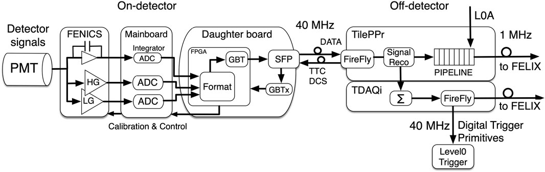
FIGURE 1. Sketch of the TileCal readout electronics and dataflow.
The amplified signals are digitized with two 12-bit ADCs in the Mainboard at 40.08 MHz, synchronously with the HL-LHC bunch crossing. The digital samples are gathered by the Daughterboard which transfers the data continuously through high-speed optical links to the TileCal PreProcessor (TilePPr) located off-detector. The TilePPr stores the high and low gain digital samples into pipeline FIFO memories. In parallel, the deposited cell energy is estimated for every bunch crossing and transmitted to the Trigger and DAQ interface (TDAQi) module. The TDAQi module builds trigger primitive objects which are transferred into the Level-0 trigger system. Upon the reception of a Level-0 acceptance signal, the selected data events are transferred to the Front End LInk eXchange (FELIX) system which implements the interface with the central ATLAS DAQ system. Moreover, the TilePPr receives and propagates to the on-detector electronics the HL-LHC synchronous clock and configuration commands. It also provides a low bandwidth data path for monitoring and control purposes.
The TileCal readout on-detector electronics is mechanically subdivided into 896 independent Minidrawer modules. The Minidrawers are equipped with 12 FENICs cards, one Mainboard and one Daughterboard and can readout up to 12 PMT channels. Thus, four Minidrawers are needed to readout the Long Barrel modules whereas only three are required for the Extended Barrel modules. Each TilePPr is connected through bi-directional optical links to 28 Daughterboards located in 4 Long Barrel and 4 Extended Barrel modules. Therefore, a total of 32 TilePPrs are needed to operate the entire TileCal detector.
2.3 The PreProcessor module requirements
The TileCal PreProcessor Module implements the interface between the on-detector electronics and the ATLAS central Data Acquisition, Detector Control (DCS) and Trigger systems. Thus, the list of requirements of the TilePPr system is defined by the overall ATLAS data acquisition, control and trigger architectures.
• The TilePPr modules must be compliant with Advanced Telecommunications Computing Architecture (ATCA), which is the standard adopted by the ATLAS collaboration to host the off-detector electronics modules for HL-LHC.
• It shall provide Intelligent Platform Management Controller (IPMC) for control and health monitoring compatible with Pigeon Point protocol.
• The space reserved to the TileCal off-detector electronics in the ATLAS Service Cavern USA15 permits the installation of a maximum of 4 14-slot ATCA shelves. Considering this constraint, a ratio of 8 detector modules (4 Long Barrel and 4 Extended Barrel) per TilePPr ATCA blade has been choosen. This implies that each TilePPr will process the data from 28 Minidrawers. Thus, a total of 32 TilePPr modules are needed to readout the 256 TileCal detector modules. The shelves shall be installed in the current vertical air cooled racks. Each rack provides space for a maximum of 2 ATCA shelves and a maximum power consumption 6 kW. Thus, the maximum power consumption per TilePPr blade shall be 400 W.
• It shall provide bi-directional high-speed optical links to communicate with the Daughterboard. The uplink is used to transmit the PMT data samples, on-detector sensors, integrator and configuration registers readback data from the Daughterboard to the TilePPr. The downlink requires low data bandwidth and it is used to propagate configuration and control commands and the synchronous HL-LHC clock from the TilePPr to the Daughterboard. Both links must have fixed and deterministic latency to synchronize the data with the trigger information. Two uplinks and one downlink are needed to process the data of each Minidrawer. Redundant link system is also a requirement to improve reliability. In total, 112 uplinks at 9.6 Gbps and 56 downlinks at 4.8 Gbps are required to process the data from 28 Minidrawers in one PPr module.
• High-speed and low latency links to communicate with the TDAQi. Each TilePPr module has to process the data from 164 cells (308 PMT channels). Assuming that it has to provide to the TDAQi the cell energy for the 17-bit dynamic range every 25 ns and some extra control and synchronization words, it implies a payload bandwidth of 120 Gbps per TilePPr module.
• It shall include a low priority communication layer for configuration and monitoring. It shall provide access to configuration registers and to the event buffers for data monitoring during data taking.
• It shall provide a dedicated ethernet connection to monitor the on-detector system health sensors data. The on-board PPr sensors data shall be accessible both from this ethernet connection and from the dedicated IPMI bus as specified in the ATCA standard
• It shall provide bi-directional communication with the FELIX system. The downlink is used to receive configuration and TTC commands and the LHC clock from the FELIX whereas the uplink is used to transmit triggered data to the FELIX. The downlink shall be implemented using the latency optimized GigaBit Transceiver (GBT) [Moreira et al. (2009)] protocol because the recovery of the LHC clock with deterministic latency is required. The uplink does not require deterministic latency but demands more data bandwidth to transmit reconstructed data for every channel and raw data for channels above a configurable threshold. A minimum of 6 Gbps is required to transmit triggered data to the FELIX system.
• It shall include a mechanism to distribute a common clock signal within the TilePPr blades installed in a shelf.
3 The PreProcessor module design
3.1 PreProcessor module conceptual design and architecture
The TilePPr module has been designed using a modular concept to optimize the design and manufacturing processes, enhance components maintenance and replaceability and facilitate future improvements in terms of functionality as shown in Figure 2. It is crucial to consider the long lifespan that these cards are expected to offer. By adopting a modular design, we can achieve several benefits. Firstly, it allows for greater flexibility and efficiency in the design process. Modules can be designed and developed independently, enabling parallel work-streams and reducing overall design time. Additionally, modules can be easily replaced or upgraded without affecting the entire system, resulting in cost savings and improved maintenance procedures. Moreover, a modular design promotes scalability and adaptability. As technology evolves and new functionalities are required, modules can be added or modified accordingly. Furthermore, modular design enhances the longevity of the TilePPr electronic card. By isolating components into separate modules, we can address issues and make improvements without the need to overhaul the entire card.
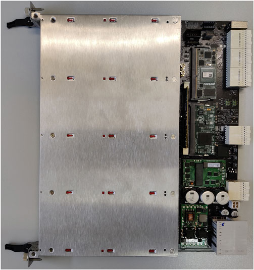
FIGURE 2. Picture of the TilePPr module.
The TilePPr is an AdvanceTCA Carrier board that supports four full-size single AMC cards as shown in Figure 3. The Carrier board provides the common clock distribution capability and up to 6 high-speed link from each AMC bay to a custom Zone 3 connector. The AMC bays host four custom Compact Processing Modules (CPMs) where the optical connections and a high performance FPGA for data processing are implemented. Each CPM processes the data from one Long Barrel and one Extended Barrel modules, i.e. 7 Minidrawers. It also implements the links to the TDAQi through the Zone 3 and to the FELIX system.
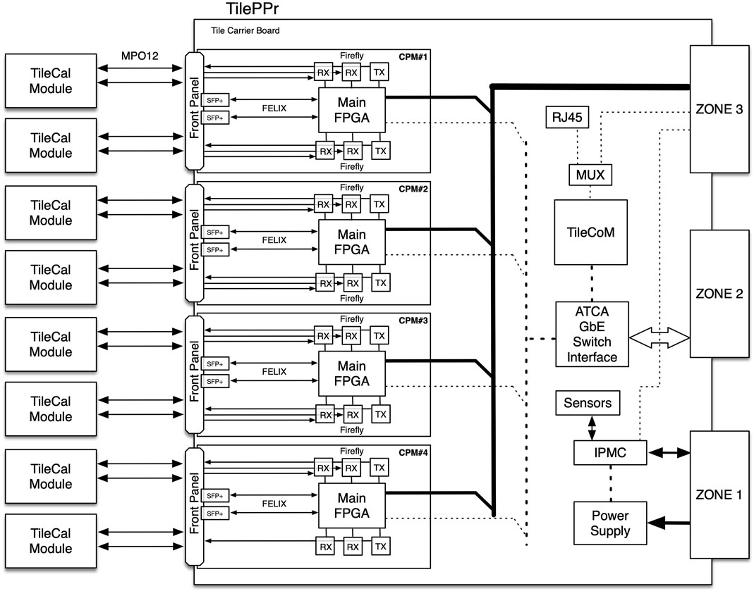
FIGURE 3. Block diagram of the TilePPr module.
In addition, the ATCA Carrier includes three SO-DIMM form factor connectors to host an IPMC, an ethernet switch and a System-On-Chip (SoC) module. The IPMC is part of the ATCA standard and it is responsible for system monitoring, management, and control functions within an ATCA chassis. The ethernet switch provides connectivity between the AMC and Zone 3 bays, the SoC module and the two Base Interface channels in the Zone 2 connector. The SoC slot can be used to control and monitor the performance of the system from a user friendly operating system.
3.2 Detailed hardware design of the PreProcessor components
3.2.1 Design of the ATCA carrier base board
The Tile ATCA Carrier Board (ACBB) has a 8U form factor mechanically compliant to PICMG ATCA 3.0 [PICMG (2008)] and AMC.0 [PICMG (2006)]. The Tile ACBB serves as the central control and connectivity hub in the ATCA system, enabling communication between AMC, SoC and Switch slots and the backplane, distributes power, managing timing, cooling, and incorporates other peripheral interfaces as shown in Figure 4. It provides the essential infrastructure and functionality required for the proper operation and management of the ATCA system. The PCB copper thickness is 35 μm and the total thickness is 2.3 mm with a total of 14 layers; 6 for signals, 6 for ground and 2 for power distribution.
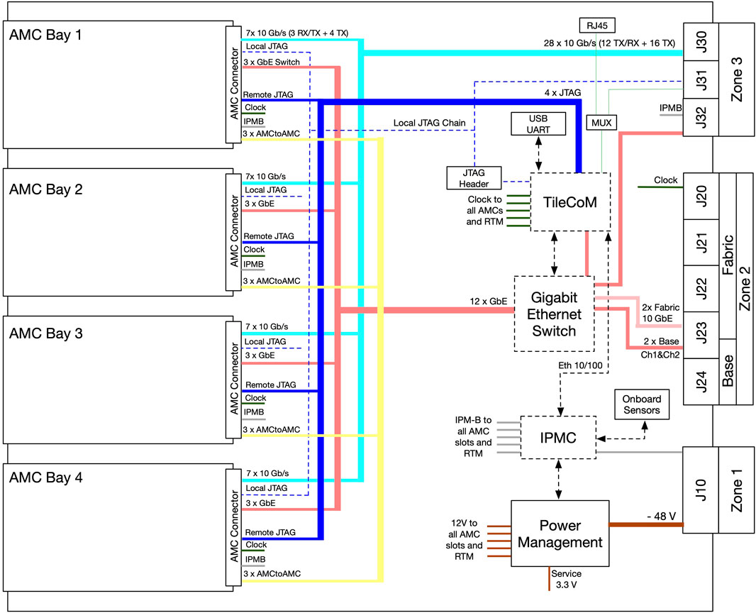
FIGURE 4. Block diagram and data flow of the Tile ACBB.
The design has been done assuming Panasonic Halogen Free MEGTRON-6 as dielectric material (dielectric constant 3.4 @ 12 GHz) for Core and PrePeg [Panasonic (2003)]. The design parameters have been optimized to obtain impedances of 50 Ω in single-line signals and 100 Ω in differential pairs. Thus, the width of lines in the external layers is 0.12 mm for single mode signals and 0.13 mm with a separation of 0.20 mm for differential pairs. In the internal layer the width of single mode signals is 0.12 mm while it is 0.12 mm and a separation of 0.2 mm for differential pairs. The copper thickness in all the layers is 35 μm.
Impedance control during fabrication is applied to Layers 3 and 12 in order to guarantee the impedance in the high-speed differential lanes connecting the AMC slots with the Zone 3 connector. These lanes are used to communicate the CPM and the TDAQi through the Zone 3 connector with a 8b/10 b encoding at 9.6 Gbps. These traces, particularly those associated with bay number 4, present considerable lengths, reaching up to 275 mm. Hence, comprehensive signal integrity studies have been performed.
3.2.1.1 Gigabit ethernet switch module
The ACBB includes a DDR3 SO-DIMM form factor socket (51 x 102 mm—204 pin) to host a switch module to interconnect the AMC bays, the SOC module and the Zone 3 connector with two channels of the Base and two channels of the Fabric interfaces buses located in the Zone 2. Figure 5 shows a picture of the baseline version of the Gigabit Ethernet (GbE) Switch Module, which is a custom designed board based on chip BCM5396 from Broadcom [Broadcom (2006)]. It implements an unmanaged 16-port GbE Switch with 3 ports connected to each AMC bay, one port to the TileCoM, one port to the Zone 3 and two ports connected to the two channels of the Base Interface. In this version the Fabric Interface is reserved for potential future upgrades of the switch module.
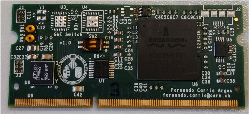
FIGURE 5. Picture of the GbE Switch module.
3.2.1.2 Tile computer system-on-chip
The Tile Computer System-On-Chip (TileCoM) is a custom designed mezzanine card in a DDR4 SO-DIMM format (69.6 x 30 mm—260 pins) [Gololo et al. (2022)]. The core of the baseline TileCoM is a Zynq FPGA (XCZU2CG) [Xilinx (2017)] including a Dual-core ARM Cortex A53 processor. It includes high-speed point-to-point connection with the AMC bays for configuration and monitoring purposes from the ARM processor. The TileCoM includes circuitry to generate and distribute a high quality clock to the AMC bays and RTM. It can also act as a master clock source in the ATCA shelf. The TileCoM is used to configure and control the ACBB. It includes a user interface running in a Linux Operating System in the ARM processor which is accessible via an Ethernet connection through the Base Interface. It provides a user friendly access to the JTAG chain in the front-end electronics through the AMC cards and the high-speed optical connection for remote programming of FPGAs in the front-end electronics. In addition, it has access to the local ACBB JTAG chain and to the temperature and current sensors.
3.2.1.3 Intelligent platform management controller
The Intelligent Platform Management Controller (IPMC) provides the interface with the Shelf Manager through the IPM-Bus in the Zone 1 connector. The IPMC is implemented with a mezzanine card designed at CERN [Mendez et al. (2017)]. It is an adaptation of the Pigeon Point IPMC which is compliant with the ATCA standard Revision 3.0.
It is a controller to manage the hot swap, Field Replaceable Units (FRU) information (AMCs and RTM) and to handle switch, LEDs, hardware address, etc. It is used to store and readout the on-board sensor to monitor temperatures, current and voltages and to detect events and send alarms. The core of the IPMC is an Microsemi A2F200 with an ARM Cortex M3 processor. Figure 6 shows all the connections between the IPMC and the components in the ACBB. The connection with the shelf manager is done through a redundant I2C connections in the Zone 1 backplane. The IPMC is powered with the 3.3 V service voltage which is available upon the insertion of the ACBB in an ATCA shelf. The IPMC enables the DC/DC converter to obtain the 12 V used in the AMC cards, RTM and payload components in the ACBB.

FIGURE 6. Picture of the CPM module.
3.3 Design of the compact processing module
Figure 6 shows the Compact Processing Module (CPM), the core of the TilePPr module. It implements the interface with the front-end electronics and the ATLAS Level-0 trigger and global data acquisition systems [Carrió (2021)]. The CPM is a single full-size Advanced Mezzanine Card (AMC) hosting one Xilinx UltraScale KU115 FPGA with 48 GTH transceivers, and 6 Samtec FireFly optical modules (Figure 7). The clock circuitry of the CPM includes a Silicon Labs si5345 jitter cleaner to obtain a high quality copy of the accelerator clock recovered from the FELIX system in order to drive the high-speed transceivers for the communication with the on-detector electronics. A Modular Management Controller (MMC) integrated with a MicroChip Atmega128A negotiates with the IPMC of the ACBB the activation of the 12 V payload power. The MMC also provides to the IPMC health monitoring data from the on-board sensors on request.
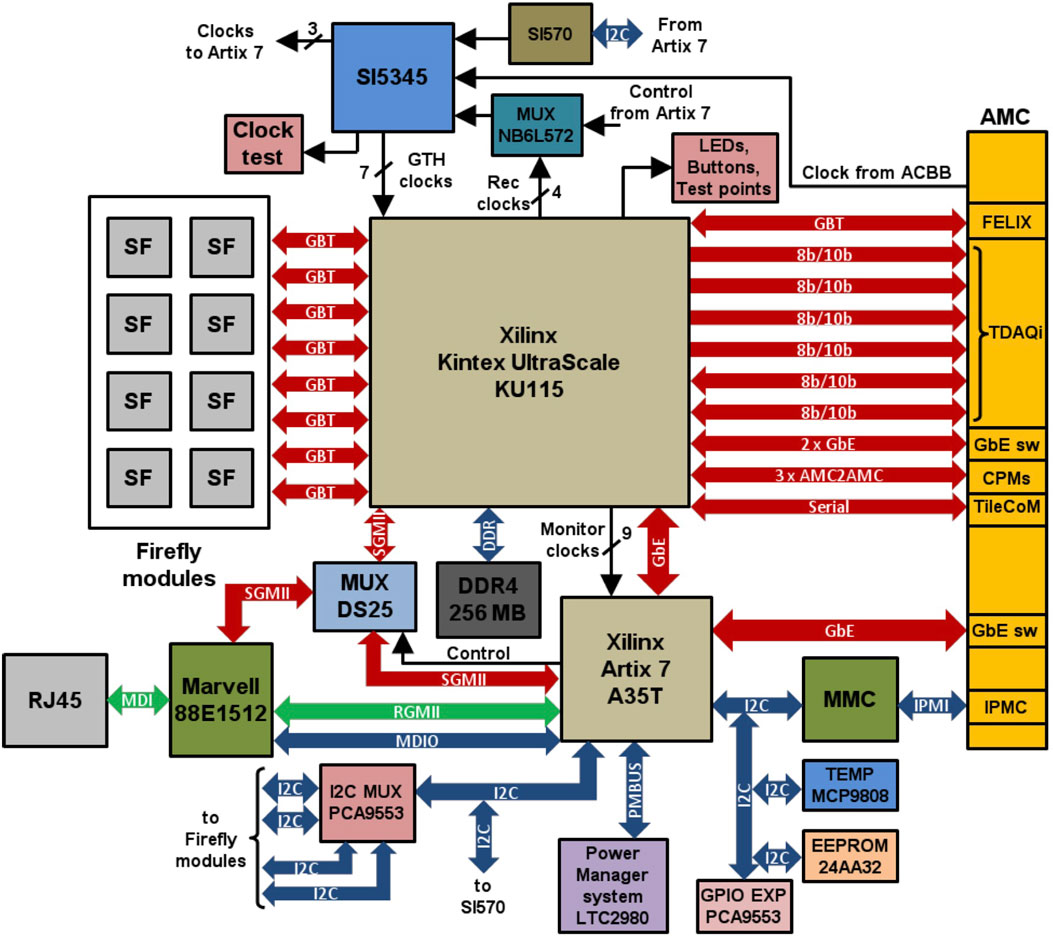
FIGURE 7. Block diagram and interfaces of the CPM.
One CPM is capable of operating up to two TileCal modules corresponding to seven Minidrawers, where each Minidrawer is operated via 4 uplinks and 2 downlinks connections. The high-speed links between the on-detector and off-detector electronics are implemented using the GBT protocol implemented in the FPGA, and they operate with fixed and deterministic latency. The DCS and configuration commands are distributed via the downlinks embedded with the accelerator clock which are used in the on-detector electronics for the digitization of the analog PMT signals. The digitized PMT signals and monitoring data are duplicated and transmitted to the TilePPr modules via redundant uplinks at a data rate of 9.6 Gbps. The Kintex UltraScale FPGA implements algorithms to provide reconstructed and calibrated energy for each cell and per every bunch crossing to the TDAQi boards.
The reconstructed cell energies are transmitted to the TDAQi board via seven links through the ACBB operating at 9.6 Gbps and using the FULL-mode protocol [Moreira et al. (2009)]. In parallel, the Kintex UltraScale FPGA stores the digitized PMT signals and the reconstructed cell energies in pipeline memories with a maximum depth of 10 μs. Upon the reception of a trigger acceptance signal from the ATLAS trigger system, the selected event is extracted from the pipeline memories and transmitted to the FELIX system through one optical link at 9.6 Gbps using the FULL-mode protocol. The CPMs also receive the Trigger, Timing and Control (TTC) information and bunch crossing clock from the FELIX system via one GBT link at 4.8 Gbps.
The PCB stack-up counts 14 layers using Panasonic Megtron6 as dielectric material [Panasonic (2003)]. Eight layers are used for control and high-speed signals, while the other six layers are devoted to power distribution. The PCB interconnects were designed to match 100 Ω for differential signals and 50 Ω for single-ended signals. The total thickness of the PCB is 1.6 mm ± 10%, being compliant with the AMC standard.
The CPM receives 12 V from the ACBB through the AMC connector. According to the ATCA standard specifications, the ACBB can deliver a maximum power of 80 W per single AMC board. An auxiliary 3.3 V is also provided to power the MMC board during the initial power negotiation between ACBB and the CPM.
The CPM power distribution system generates twelve different voltages from +12 V for the operation of the FPGAs and rest of components.
3.4 Firmware overview and functionality
3.4.1 Tile computer system-on-chip
The TileCoM SoC firmware includes the boot and runtime firmware for the ARM processor and the custom VHDL IP cores. The boot firmware handles the initialization of the hardware and loads the runtime firmware which is based on an ALMA Linux Operating System. This runtime OS provides a user friendly interface for low priority functionalities. The system is accessed through a GbE connection through the Zone 2 Base Interface. Additionally, there is a direct GbE connection from a connector in the ACBB or through the Zone 3 backplane. The tasks that can be executed during runtime include the Xilinx Virtual Cable for JTAG programming of ACBB and on-detector programmable devices. It also implements an Open Platform Communications (OPC) Unified Automation (UA) server which acts as a central hub that collects and organizes data from diverse sensors both in the ACBB and in the on-detector electronics. It represents the interface with the DCS system, enabling real-time monitoring, control, and analysis of the system health.
3.5 IPMC
The IPMC firmware is a CERN adaptation based on the Pigeon Point solution. It provides the basic system functionalities to communicate with the Shelf Manager and the hot swap controllers of the AMC bays and the RTM. The software layer, executed in the embedded cortex-M3 processor, is used to customize the functionalities for the ACBB. It implements the drivers to communicate with the on-board temperature and power consumption sensors and with the 12 V power regulator.
3.6 Compact processing module
The CPM MainFPGA is responsible for handling the detector data processing operations efficiently and effectively. The firmware project implements different processing layers that are executed concurrently.
The critical data path to the trigger system imposes a stringent requirement for low, fixed and deterministic latency. The total ATLAS Level-0 trigger latency is 10 μs with a maximum contribution for the Tile readout path of 1.7μs. Table 1 shows the latency introduced during the different processing steps in the readout path. The signal produced in the detector is digitized and transmitted to the TilePPr through optical links. Then, the digital samples are reconstructed to obtain the energy deposited in the cell. The result is transmitted to the TDAQi where the trigger primitives are built and forwarded to the different trigger systems.
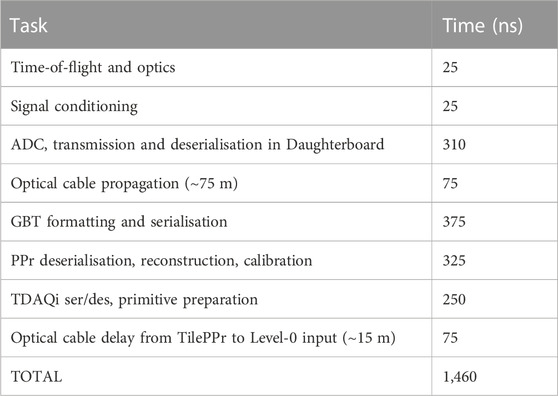
TABLE 1. Readout path tasks with latency.
Currently several studies about real time signal reconstruction techniques and algorithms are ongoing. The evaluation aims to identify algorithms that can effectively reconstruct signals within the required timeframe despite the limited processing time available imposed by the Level 0 latency. The Optimal Filtering algorithm [Valero et al. (2007)], which has been used in the TileCal RODs during the LHC operation, has been implemented in the CPM MainFPGA. However, the utilization of FPGAs instead of the Digital Signal Processors (DSPs) used in the RODs, permits the implementation of more sophisticated algorithms. Machine Learning methods have been implemented with excellent results especially in high pileup environments [Arciniega et al. (2019)].
The serial links to communicate with the front-end use the CERN custom GBT protocol implemented in the FPGA firmware. The communication links are controlled from a data encoder and decoder blocks which organize the information in the protocol payload.
In parallel with the trigger path, the data samples are stored in the internal FPGA memory. The data must be stored for the Level-0 trigger latency of 10 μs duration. Considering the sample rate of 40 MHz, this results in a memory capacity of 400 12-bit samples for each channel and gain. Moreover, the reconstructed energy per channel is also stored in the pipeline memories. Upon the reception of a Level-0 trigger acceptance signal, the reconstructed energy and the digital samples are transmitted to the FELIX system for further processing.
The CPM MainFPGA is controlled via the IPbus protocol, which is an ethernet-based control system designed for handling the data transaction between FPGA-based ATCA systems and computers [Williams (2014)]. The FPGAs are controlled through the mapping of a virtual 32-bit address space to 32-bit registers. The IPbus protocol supports individual read and write operations on all the registers in the FPGAs. This permits the control, configuration and monitoring of the MainFPGA processes and also to the front-end electronics through the high-speed optical links. In addition, it provides access to the internal pipeline memories for event sampling monitoring and for low priority readout tasks.
Table 2 presents an estimation of the resource occupancy of the Kintex UltraScale FPGA based on a preliminary version of the firmware project including all the functionalities required. The firmware is expected to undergo continuous evolution, with particular emphasis on ongoing research to optimize signal reconstruction algorithms. Furthermore, the presence of unused resources ensures the potential for future upgrades, thus enabling further enhancements to be incorporated.

TABLE 2. CPM MainFPGA list of resources available and estimated usage.
4 Certification tests
4.1 Description of specific tests required for certification
The certification of the TilePPr module design, involved specific tests to ensure its compliance with industry standards, integration with other readout components and functional requirements. Four prototypes were produced and used during the design certification.
Firstly, several tests were performed to certify the compliance with ATCA-specific standards. This involved validating its adherence to physical design and form factor requirements, ensuring proper mechanical integration within the ATCA chassis. It was also verified that the module efficiently manages power consumption and dissipates heat to maintain reliable operation within the system.
Certification also entailed comprehensive functional testing to validate system control, configuration and monitoring features. In particular, the correct performance of the GbE communication with the CPMs through the GbE Switch module was verified. Dedicated software libraries and graphical user interface tools were deployed to perform systematic verification tests for the configuration and data readout through the IPbus interface. These tools permits to ensure the interoperability within the readout chain and verifies the correct integration with the rest of the electronics modules in the data acquisition system.
In the certification process of the TilePPr module, the high-speed communication links were validated with eye diagram analysis and Bit Error Rate (BER) tests using the Xilinx IBERT Tool. It implied the fiber optics communication with the on-detector electronics and the data transmission to the FELIX and trigger systems. First, the bi-directional communication with the Daughterboard located in the on-detector through 100 m optical fibers was validated using the baseline GBT protocol running at 9.6 Gbps in the uplink and 4.8 Gbps in the downlink. Then, a crucial test was conducted to verify the correct signal integrity during communication between the AMC bays and Zone 3. These lanes, which can be significantly long, reaching up to 275 mm, carry high-speed signals on the order of 10 Gbps. This test ensures the seamless and reliable transmission of signals over these extended distances, validating the module’s performance and compatibility within the ATCA system.
Overall, the certification of the TilePPr module design involved a range of specific tests to ensure its compliance with industry standards, performance requirements, and interoperability within the ATLAS data acquisition ecosystem. Through these tests, the module’s capabilities, reliability, and compatibility are thoroughly assessed, providing assurance of its suitability for installation in the ATLAS experiment.
4.2 Considerations for compliance with ATCA-specific standards
Compliance with ATCA-specific standards necessitates ATCA modules to fulfill various essential functionalities. Firstly, they must adhere to the defined physical design and form factor, ensuring proper mechanical integration within the ATCA chassis. In the ACBB case, it has an ATCA carrier blade form factor including a cut-away zone under the AMC bays as specified in the ATCA standard. The mechanical integration is implemented with a commercial Carrier Mechanics for Full-Size AdvancedMC modules provided from Schroff. It provides a mechanical structure to enhance the robustness of the board specially in the cutaway area, handles for hot swap insertion and extraction and guides for the AMC slots.
Backplane communication support is imperative for high-speed data exchange between modules within the ATCA system, necessitating compliance with the specified signaling protocols. The Zone 2 is devoted to provide Ethernet access to every TilePPr module inserted in the ATCA shelf. A custom ATCA switch blade has been designed to be installed in a hub slot. It is used as a gateway to the Zone 2 bus. The Zone 3 is custom defined and it is used to communicate with the RTM module inserted in the back of the shelf.
Efficient management of power consumption and heat dissipation is crucial to guarantee reliable operation and resource utilization. Comprehensive management and monitoring capabilities are essential for system-level control, configuration, and diagnostics. ATCA modules should comply with the Intelligent Platform Management Interface (IPMI) standard, enabling remote monitoring, management, and control of ATCA systems. Redundancy and fault tolerance mechanisms are vital to ensure system availability and reliability. Modules must provide features like redundant power supplies, hot-swappable components, and fault detection mechanisms. The CERN launched a project dedicated to the study of the impact of the ATCA integration in the actual counting rooms and to analyze the impact on the cooling infrastructures [Bortolin et al. (2018)]. The system monitoring is implemented in the TilePPr with the CERN IPMC module, which is a common solution for ATCA systems developed for the HL-LHC.
4.3 Certification of the CPM optical communication
The optical links of the CPM have undergone qualification tests using the Xilinx IBERT IP core [Xilinx (2018)]. The tests involved running the links at a speed of 9.6 Gbps and conducting Bit Error Rate (BER) tests.
In order to evaluate the performance, two separate CPMs were utilized in the setup. Over a period of 7 days, these CPMs transmitted and received data patterns of 231 − 1 Pseudo-Random Bit Sequence (PRBS31). The results of the tests indicated that no errors were detected in any of the links. The individual links achieved a BER better than 5 ⋅ 10−16 with a Confidence Level (CL) of 95%, while the combined BER of all links reached a value better than 1.6 ⋅ 10−17 with a CL of 95%. Therefore, the data transmission was found to be highly reliable.
During the testing process, the power consumption measured was approximately 32 W. However, it is expected that the power consumption of the CPM will increase by 12 W during actual operation due to additional firmware functions. This estimation was based on the Xilinx Power Estimator tool and the anticipated resource utilization of the final firmware. Despite this increase, the total power consumption of the CPM is projected to remain within the power consumption budget of 60 W per AMC specified by the ATCA standard.
As part of the validation tests for the CPMs, the signal integrity was assessed by measuring the eye diagrams at the output of the Samtec FireFly modules. The measurements were performed at data rates of 4.8 Gbps and 9.6 Gbps using a DCA-X 86100D sampling oscilloscope from Keysight. The obtained eye diagrams, shown in Figure 8, exhibited wide openings without significant jitter, indicating satisfactory noise margins.
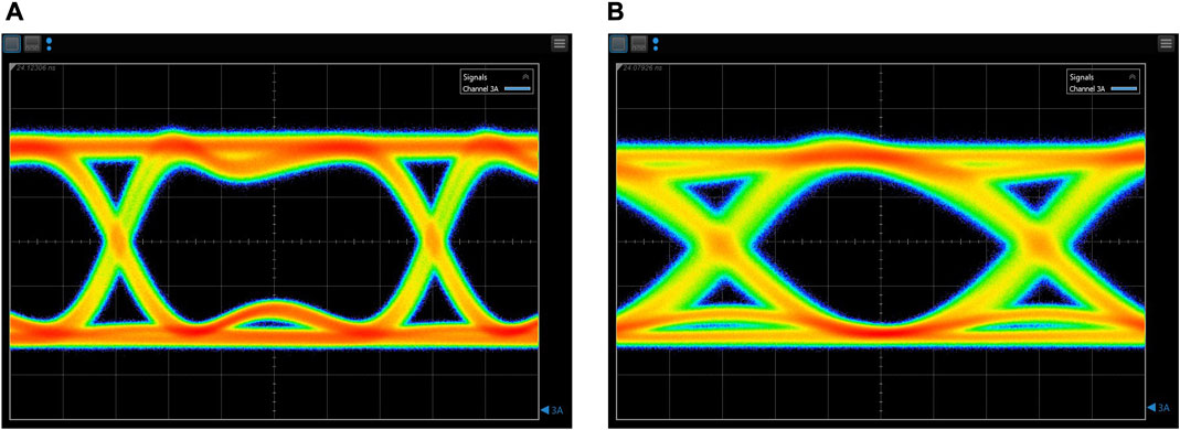
FIGURE 8. Measured output eye diagrams for 4.8 Gbps (A) and 9.6 Gbps (B) data rates.
Signal quality parameters were extracted from the measured eye diagram data. Table 3 provides a summary of the extracted values for jitter, eye height, and eye width at both 4.8 Gbps and 9.6 Gbps data rates.
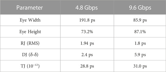
TABLE 3. Signal quality parameters derived from the eye diagrams at 4.8 Gbps and 9.6 Gbps.
4.4 Certification of high-speed communication between AMC bays and zone 3 backplane
One of the most critical tests in the certification process of the TilePPr module is the verification of high-speed communication between the AMC bays and the Zone 3 backplane. This test is of utmost importance as it ensures the reliable and efficient transmission of trigger information from the FPGA in the CPMs to the FPGA in the TDAQi located in the Zone 3 connector. Each AMC bay includes 7 lanes to transmit data to the TDAQi which use an 8b/10 b encoding at 9.6 Gbps. In the oposite direction there are 3 lanes per AMC bays which also use 8b/10 b encoding at 4.8 Gbps. Different dielectric materials were evaluated for the PCB fabrication. Figure 9 shows the impedance of the longest differential trace in the PCB connecting AMC bay 4 and the Zone 3 connector for FR4 and Megtron6 Panasonic ultra-low transmission dielectric material. In addition, the Megtron6 PCB has been manufactured with controlled differential impedance of 100 Ω. The impedance has been measured with the Time Domain Reflectometer of the Keysight DCA-X 86100D oscilloscope. The impedance of the MEGTRON6 PCB shows a differential impedance very close to 100 Ω and with discontinuities below 5% throughout the connection between the AMC slot and the TDAQi module. The PCB with FR4 present an impedance in the ACBB above 120 Ω with a drop to 100 Ω in the connection to the TDAQi. Thus, Megtron6 from loss dielectric material was selected, including impedance control during PCB manufacturing to assure optimum data transmission specially in the long traces.
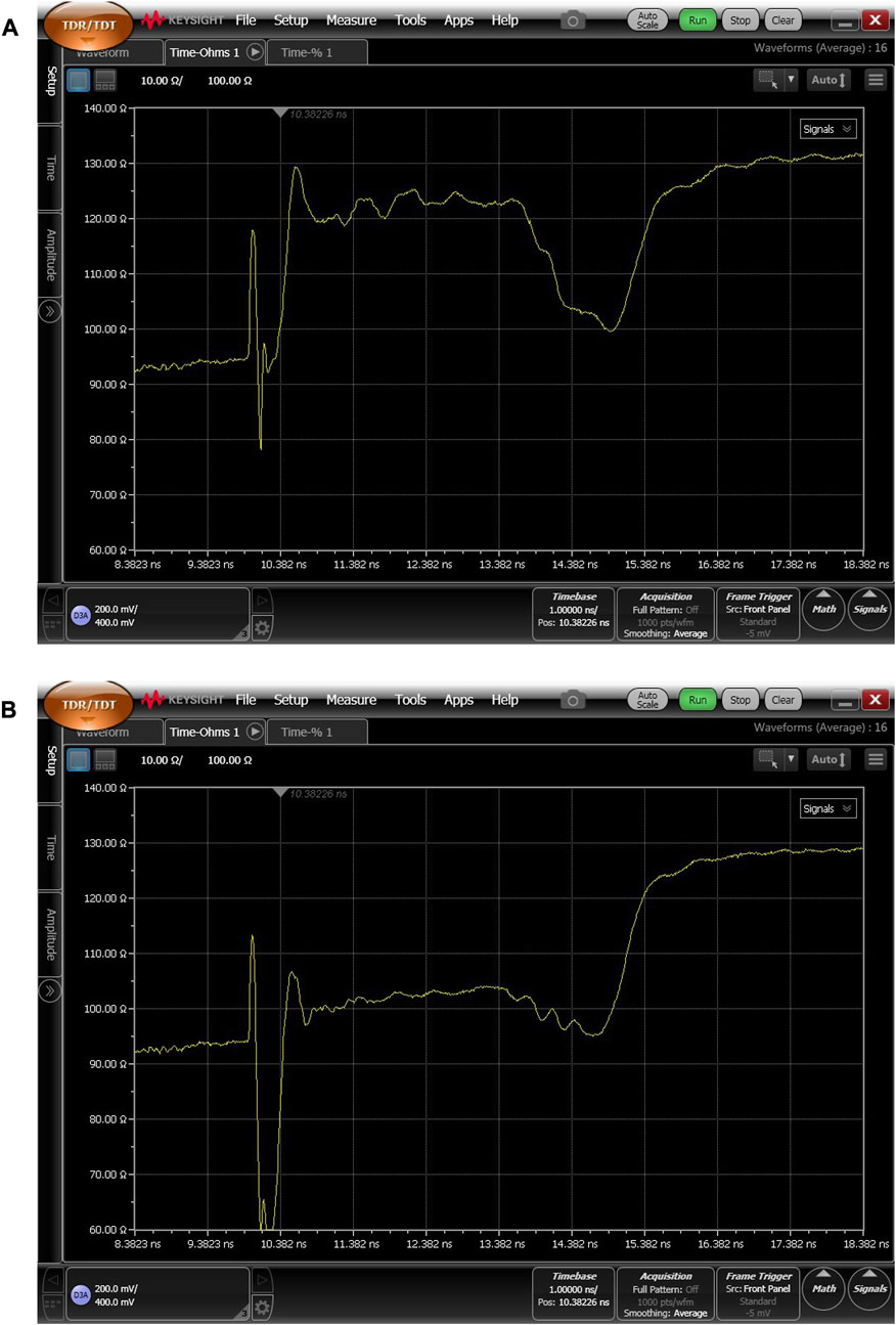
FIGURE 9. Differential impedance of the longest trace connecting AMC bay 4 and the TDAQi plugged in the Zone 3. (A) PCB with FR4 dielectric material and non-controlled impedance during manufacturing. (B) PCB with MEGTRON6 dielectric material and impedance control during manufacturing.
In addition, Bit Error Rate (BER) tests were performed on every lane using the Xilinx IBERT tool. In order to emulate the 8b/10 b encoding pattern, a PRBS-7 generator was used. The links were validated with an aggregated BER better than 2 × 10⁻¹⁷ with a Confidence Level of 95%.
5 Conclusion
The TilePPr module design incorporates a modular approach, offering benefits such as optimized design processes, enhanced maintenance, and the potential for future improvements. The module underwent specific tests to ensure compliance with industry standards, functional requirements, and integration within the ATCA system. Certification involved validating physical design, form factor adherence, power management, and heat dissipation. Functional tests verified system control, configuration, and monitoring features, including GbE communication and data readout. High-speed communication links were validated through eye diagram analysis and BER tests.
Compliance with ATCA-specific standards required adherence to physical design, form factor, backplane communication support, power management, and fault tolerance mechanisms. The module successfully met these standards, including the use of a custom GbE Switch Module and a TileCoM for system control and connectivity. The IPMC facilitated system monitoring, management, and control functions.
The Compact Processing Module (CPM) served as the core of the TilePPr module, implementing high-speed links and communication with on-detector electronics. Impedance control and dielectric material selection ensured optimum data transmission in the high-speed lanes. The successful completion of tests provided assurance of the module’s compliance, reliability, and compatibility within the ATCA system.
The comprehensive certification process ensured the module’s suitability for installation in the ATLAS experiment, meeting the demanding requirements of data acquisition and integration within the ATCA ecosystem.
Data availability statement
The original contributions presented in the study are included in the article/supplementary material, further inquiries can be directed to the corresponding author.
Author contributions
AV: Conceptualization, Funding acquisition, Investigation, Project administration, Supervision, Writing–original draft, Writing–review and editing. FC: Conceptualization, Formal Analysis, Investigation, Methodology, Software, Validation, Writing–original draft. LF: Conceptualization, Funding acquisition, Project administration, Resources, Supervision, Writing–review and editing. AC: Formal Analysis, Investigation, Software, Validation, Writing–review and editing. DH: Investigation, Software, Validation, Writing–review and editing. AR: Conceptualization, Funding acquisition, Project administration, Resources, Writing–review and editing.
Funding
The author(s) declare financial support was received for the research, authorship, and/or publication of this article. This work is supported by the Ministerio de Ciencia e Innovación (Spain) projects (RTI 2018-094270-B-I00 and PID 2021-125069OB-I00) and by Plan Complementario de I+D+i—Plan de Recuperación, Transformación y Resiliencia 2022 (ASFAE/2022/008). Generalitat Valenciana, Ministerio de Ciencia e Innovación, Unión Europea NextGenerationEU.
Conflict of interest
The authors declare that the research was conducted in the absence of any commercial or financial relationships that could be construed as a potential conflict of interest.
The authors declared that they were an editorial board member of Frontiers, at the time of submission. This had no impact on the peer review process and the final decision.
Publisher’s note
All claims expressed in this article are solely those of the authors and do not necessarily represent those of their affiliated organizations, or those of the publisher, the editors and the reviewers. Any product that may be evaluated in this article, or claim that may be made by its manufacturer, is not guaranteed or endorsed by the publisher.
Footnotes
1ATLAS uses a right-handed coordinate system with its origin at the nominal interaction point (IP) in the centre of the detector and the z-axis along the beam pipe. The x-axis points from the IP to the centre of the LHC ring, and the y-axis points upward. Cylindrical coordinates (r, ϕ) are used in the transverse plane, ϕ being the azimuth angle around the z-axis. The pseudorapidity is defined in terms of the polar angle θ as η = −ln tan(θ/2).
References
Arciniega, J. O., Carrió, F., and Valero, A. (2019). Fpga implementation of a deep learning algorithm for real-time signal reconstruction in particle detectors under high pile-up conditions. J. Instrum. 14, P09002. doi:10.1088/1748-0221/14/09/P09002
ATLAS Collaboration (2008). The ATLAS experiment at the CERN Large hadron collider. JINST 3, S08003. doi:10.1088/1748-0221/3/08/S08003
ATLAS Collaboration (2012). Observation of a new particle in the search for the standard model Higgs boson with the atlas detector at the lhc. Phys. Lett. B 716, 1–29. doi:10.1016/j.physletb.2012.08.020
Bortolin, C., Dyngosz, D., Kalinowski, M., Koziol, P., Mendez, J., Walerianczyk, J., et al. (2018). “Atca - thermal management study for the atlas phase ii upgrades,” in Proceedings of topical workshop on electronics for particle physics — PoS(TWEPP-17), 112. doi:10.22323/1.313.0112
Carrió, F. (2021). Design of the compact processing module for the atlas tile calorimeter. IEEE Trans. Nucl. Sci. 68, 1944–1951. doi:10.1109/TNS.2021.3085490
Chatrchyan, S., Hmayakyan, G., Khachatryan, V., Sirunyan, A. M., Adam, W., Bauer, T., et al. (2008). The CMS experiment at the CERN LHC. JINST 3, S08004. doi:10.1088/1748-0221/3/08/S08004
Gololo, M., Carrió Argos, F., and Mellado, B. (2022). Tile computer-on-module for the atlas tile calorimeter phase-ii upgrades. J. Instrum. 17, P06020. doi:10.1088/1748-0221/17/06/P06020
Mendez, J., Bobillier, V., Haas, S., Joos, M., Mico, S., and Vasey, F. (2017). Design of an advancedtca board management controller (ipmc). J. Instrum. 12, C03010. doi:10.1088/1748-0221/12/03/c03010
Moreira, P., Ballabriga, R., Baron, S., Bonacini, S., Cobanoglu, O., Faccio, F., et al. (2009). The GBT project. doi:10.5170/CERN-2009-006.342
Panasonic (2003). Ultra-low transmission loss Highly heat resistant Multi-layer circuit board materials MEGTRON6. Tech. rep.
Valero, A., Abdallah, J., Castillo, V., Cuenca, C., Ferrer, A., Fullana, E., et al. (2007). “Dsp online algorithms for the atlas tilecal read-out drivers,” in 2007 15th IEEE-NPSS real-time conference, 1–7. doi:10.1109/RTC.2007.4382840
Williams, T. S. (2014). IPbus A flexible Ethernet-based control system for xTCA hardware. Tech. rep. Geneva: CERN.
Keywords: FPGA, PCB design, readout electronics, ATCA, IPMI, system-on-chip, LHC, ATLAS
Citation: Valero A, Carrió F, Fiorini L, Cervelló A, Hernandez D and Ruiz Martinez A (2023) The PreProcessor module for the ATLAS Tile calorimeter at the HL-LHC. Front. Detect. Sci. Technol 1:1264123. doi: 10.3389/fdest.2023.1264123
Received: 20 July 2023; Accepted: 06 September 2023;
Published: 19 September 2023.
Edited by:
Cristina Fernández Bedoya, Centro de Investigaciones Energéticas, Medioambientales y Tecnológicas, SpainReviewed by:
A. Gabrielli, University of Bologna, ItalyGianluca Traversi, University of Bergamo, Italy
Copyright © 2023 Valero, Carrió, Fiorini, Cervelló, Hernandez and Ruiz Martinez. This is an open-access article distributed under the terms of the Creative Commons Attribution License (CC BY). The use, distribution or reproduction in other forums is permitted, provided the original author(s) and the copyright owner(s) are credited and that the original publication in this journal is cited, in accordance with accepted academic practice. No use, distribution or reproduction is permitted which does not comply with these terms.
*Correspondence: A. Valero, YWxiZXJ0by52YWxlcm9AY2Vybi5jaA==