 Philipp Maier
 Noah. J. Hourigan
 Adrian Ruckhofer1
 Anton Tamtögl
94% of researchers rate our articles as excellent or good
Learn more about the work of our research integrity team to safeguard the quality of each article we publish.
Find out more
ORIGINAL RESEARCH article
Front. Chem., 16 November 2023
Sec. Chemical Physics and Physical Chemistry
Volume 11 - 2023 | https://doi.org/10.3389/fchem.2023.1249290
This article is part of the Research TopicDynamics at Surfaces: Understanding Energy Dissipation and Physicochemical Processes at the Atomic and Molecular LevelView all 13 articles
We present a detailed helium atom scattering study of the charge-density wave (CDW) system and transition metal dichalcogenide 1T-TaS2. In terms of energy dissipation, we determine the electron-phonon (e-ph) coupling, a quantity that is at the heart of conventional superconductivity and may even “drive” phase transitions such as CDWs. The e-ph coupling of TaS2 in the commensurate CDW phase (λ = 0.59 ± 0.12) is compared with measurements of the topo-logical insulator TlBiTe2 (λ = 0.09 ± 0.01). Furthermore, by means of elastic He diffraction and resonance/interference effects in He scattering, the thermal expansion of the surface lattice, the surface step height, and the three-dimensional atom-surface interaction potential are determined including the electronic corrugation of 1T-TaS2. The linear thermal expansion coefficient is similar to that of other transition-metal dichalcogenides. The He−TaS2 interaction is best described by a corrugated Morse potential with a relatively large well depth and supports a large number of bound states, comparable to the surface of Bi2Se3, and the surface electronic corrugation of 1T-TaS2 is similar to the ones found for semimetal surfaces.
While it has long been known that the weak short-range van der Waals (vdW) interaction holds together layered materials like graphite and MoS2 (Fiedler et al., 2023), with the availability of graphene by the so-called scotch tape technique, a vast class of two-dimensional (2D) materials has been investigated (Duong et al., 2017). Mechanical cleavage can be used to prepare monolayers of vdW layered materials, a preparation technique that also works for the layered class of 3D topological insulators (TIs), and first attempts to use these materials in vdW heterostructures and devices are described in Liu et al. (2016). The well-known physics and chemistry of three-dimensional bulk matter often become irrelevant for 2D materials, revealing exotic phenomena in vdW-layered crystals (Duong et al., 2017). Among the most prominent 2D materials are the semimetal graphene, and the transition metal dichalcogenides (TMdCs), which tend to be semiconductors. Here, we provide a detailed helium atom scattering (HAS) study of the TMdC and archetypal charge-density wave (CDW) system 1T-TaS2 (Rossnagel, 2011). The electron-phonon coupling of the latter is further compared with measurements of the topological insulator TlBiTe2, which in contrast exhibits a stronger bonding between the layers. Scattering and diffraction from both surfaces are compared in terms of interlayer bonding and surface quality, and completed with measurements of the thermal expansion and a determination of the three-dimensional atom-surface interaction potential of 1T-TaS2.
TMdCs are atomically thin semiconductors of the type MCh2, with M being a transition metal atom and Ch a chalcogen atom, where one layer of M atoms is sandwiched between two layers of Ch atoms [see Figure 1A (Duong et al., 2017)]. A TMdC with a particular rich phase diagram is TaS2. The phase diagram of the 1T polytype of TaS2 (Figure 1A) involves several CDW transitions driven by strong electronic correlations and electron-phonon (e-ph) coupling upon changes of the surface temperature (Tsen et al., 2015; Vaskivskyi et al., 2015). No final agreement on the electronic ground state of the material or the role of correlations has been reached, and it has even been suggested that the existing experimental evidence for 1T-TaS2 is consistent with the ground state being a quantum spin liquid (Klanjšek et al., 2017; Law and Lee, 2017).
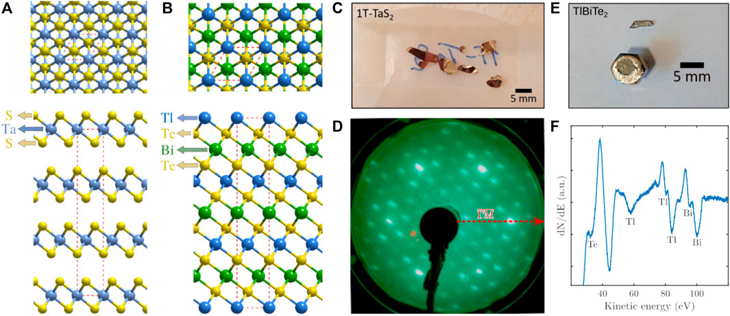
FIGURE 1. Top and side view of (A) 1T-TaS2(0001) and TlBiTe2(111) (B). (C) Image of the as-grown 1T-TaS2 crystals. (D) shows the low energy electron diffraction (LEED) pattern of 1T-TaS2 with the sample aligned along the high symmetry
TlBiTe2 on the other hand is a trigonal crystal with 4 layers as shown in Figure 1B forming a repeated elemental sequence (Tl-Te-Bi-Te-Tl) and TlBiTe2 as well TlBiSe2 are thallium-based ternary narrow-band semiconductors (Singh et al., 2016). It was predicted theoretically that this class of materials are 3D TIs (Eremeev et al., 2010; Eremeev et al., 2011; Lin et al., 2010; Yan et al., 2010), later followed by experimental evidence of its topological properties (Chen et al., 2010; Kuroda et al., 2010; Kuroda et al., 2013). Chen et al. measured the 3D band structure of TlBiTe2 using angle-resolved photoemission spectroscopy (ARPES) and found a single Dirac cone in the center of the surface Brillouin zone (Chen et al., 2010; Singh et al., 2012). Due to the observation of the negative bulk band gap of −10 meV they concluded that TlBiTe2 may be classified as a semimetal rather than a narrow-gap semiconductor as suggested by theory and that this semimetallic nature explains its small thermoelectric power (Spitzer and Sykes, 1966; Kurosaki et al., 2003; Chen et al., 2010). Furthermore, according to Singh et al., Weyl semimetals can be realized at the topological critical point in alloys TlBi(S1−xTex)2 by breaking the inversion symmetry in layer-by-layer growth in the order Tl-Te-Bi-S (Singh et al., 2012). However, such kind of structures have not been realized so far.
Similar to 1T-TaS2 and the 3D TI family Bi2Te3/Bi2Se3, where the quintuple layers are weakly bound by vdW interactions (Zhang et al., 2009), TlBiTe2 is also a layered material but its atomic layers are bonded covalently (Yan et al., 2010). While the e-ph coupling has been measured for a variety of TIs in particular the class of binary TIs (Ruckhofer et al., 2020), much less experimental information about the TlBiTe2 system is available not least in terms of the e-ph coupling.
HAS is ideally suited to study CDW phases since the neutral He beam is directly scattered by the surface electrons and HAS permits determination of the e-ph coupling λ (Manson et al., 2022) which specifies also conventional superconductivity (Benedek et al., 2020b). Previous HAS diffraction and phase transition data from HAS are described in Benedek et al. (2020b), including CDW systems with HAS (Tamtögl et al., 2019; Ruckhofer et al., 2023).
Our experiments were performed at the HAS apparatus in Graz. A detailed description of the experimental setup has been given elsewhere (Tamtögl et al., 2010). A nearly monochromatic beam (ΔE/E ≈ 2%) of 4He which is generated by a supersonic expansion through a cooled 10 μm nozzle, passes through a skimmer and is scattered off the sample surface. By varying the nozzle temperature, the beam energy of the incident helium beam can be tuned between 9 and 20 meV. In our setup, the angle between the source arm and the detector arm is fixed at 91.5°. After hitting the sample in the main chamber under ultra-high vacuum (UHV) conditions (p < 2 ⋅ 10–10 mbar) the beam is detected using a quadrupole mass spectrometer. By rotating the sample, the angle of incidence ϑi can be varied.
TaS2 crystals were grown by chemical vapor transport using I2 as transport agent and the 1T-TaS2 phase was obtained by quenching the crystals from
The TlBiTe2 sample was grown in the group of C. Felser (Li et al., 2017; Pei et al., 2022). Due to the stronger bonding between the layers as illustrated in Figure 1B, cleaving requires knocking off an attached post in situ in the mentioned transfer chamber. The latter had been attached with epoxy prior to transferring the sample into the transfer chamber. Figure 1E shows an image of the post with the remaining attached crystal after it had been removed from the chamber.
Following cleavage, both samples can be inserted into the scattering chamber. For temperature-dependent measurements, the sample can be cooled down to 115 K via a thermal connection to a liquid nitrogen reservoir and heated using a button heater.
Figures 1A, B illustrate the structures of both 1T-TaS2 and TlBiTe2. As mentioned in the introduction, it is evident from the side view of TlBiTe2 that the coupling between the atomic layers is much stronger and less of a vdW type compared to the TMdCs but also compared to bonding between the quintuple layers of the binary TIs. The latter is actually confirmed in our experiments as TlBiTe2 is much more difficult to cleave as mentioned above. In the Auger electron spectroscopy (AES) spectrum shown in Figure 1F mostly the main peaks from Tl and Bi are present, the peak at about 45 eV stems most likely from elements in the sample holder. As said above, TlBiTe2 is a trigonal crystal but similar to the binary TIs it is more convenient to consider them in the conventional hexagonal notation (red dashed line in Figure 1B) with c = 3c0, i.e. three repeated elemental sequences. These repeatable sequences, consisting of four layers each, are however compared to the quintuple layers in the binary TIs not separated by a vdW gap.
The surface termination of TlBiSe2 has been studied experimentally by Kuroda et al. using scanning tunneling microscopy (STM) and core-level photoelectron spectroscopy (CL-PES) (Kuroda et al., 2013) and by Pielmeier et al. using ARPES, X-ray photoelectron spectroscopy (XPS), STM and atomic force microscopy (AFM) (Pielmeier et al., 2015). Both studies agree that cleaving happens between Tl and Se layers since the bonding strength between these layers is weaker compared to other layers according to ab initio calculations (Eremeev et al., 2011). Their STM and CL-PES results showed that after cleavage the surface is terminated by a Se layer with islands of Tl atoms on top of the Se layer covering roughly half of the surface which is further supported by ab initio calculations for TlBiSe2 and TlBiTe2 (Singh et al., 2016). Following the reports which suggest a rough, nonpolar surface model (Kuroda et al., 2013; Singh et al., 2016) it appears likely that the same scenario holds for TlBiTe2, i.e., a Te layer covered by Tl islands forms the termination after cleavage. In fact the inset of Figure 2B which shows the first order diffraction and the specular along
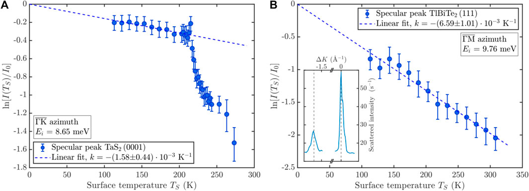
FIGURE 2. The temperature dependencies of the Debye-Waller exponents of (A) 1T-TaS2 for the specular peak with the sample aligned along
After cleavage of 1T-TaS2 on the other hand we can clearly resolve the first order diffraction peaks as illustrated in Figure 3, both at room temperature as well as for the cooled sample. The complex CDW structure of 1T-TaS2, as described by Wilson et al. (Wilson et al., 1975; Wilson et al., 2001; Coleman et al., 1992), and more recently by (Yu et al., 2015) has previously been studied with HAS by (Cantini et al., 1980) and Brusdeylins et al. (Brusdeylins et al., 1989; Benedek et al., 2020b). Here we concentrate on a more detailed study and analysis of the nearly commensurate and commensurate CDW phase of 1T-TaS2. As described in recent transport measurements, upon cooling 1T-TaS2 sequentially enters an incommensurate CDW (I-CDW) phase below 550 K, a nearly commensurate CDW (NC-CDW) phase below 350 K, and finally a commensurate CDW (C-CDW) phase below 180 K (Wang et al., 2020). When comparing the cooling and heating data a hysteretic behavior is typically observed both in resistivity (Wang et al., 2020) as well as in HAS measurements (Benedek et al., 2020b). Moreover, upon heating, 1T-TaS2 enters a triclinic CDW (T-CDW) phase at 220 K, followed by the NC-CDW phase at 280 K (Wang et al., 2020). The space modulations of different CDWs form so-called star-of-David clusters which can be clearly seen in the low energy electron diffraction (LEED) pattern in Figure 1D. In the C-CDW phase, the star of David clusters cover the entire lattice, forming a commensurate
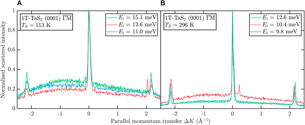
FIGURE 3. Diffraction scans of TaS2 at surface temperatures of (A) TS = 113 K and (B) TS = 296 K both in
In general, weakly coupled layered structures such as TaS2 have many polymorphs with different stackings and the contrasting behavior between both investigated samples becomes evident from the Debye-Waller plot in Figure 2. TlBiTe2 exhibits only one phase within the covered temperature region and shows the typical linear decrease of the specular intensity. For 1T-TaS2 on the other hand, upon heating, the typical linear decrease of the specular intensity within the commensurate CDW phase is followed by a small increase upon entering the triclinic CDW phase at around 210 K and an abrupt decrease with a further transition to the incommensurate CDW phase around 270 K. In the following, we describe how HAS permits to determine the e-ph coupling and compare the obtained values for both systems.
A convenient parameter to characterize the e-ph coupling strength is the mass-enhancement λ (Grimvall, 1981). Since the e-ph coupling describes the interaction between the electronic system and the lattice dynamics (phonons), experimental studies at finite temperatures can either concentrate on the electronic or the phononic system. The former is mostly available via ARPES by examining the renormalization of the electron energy dispersion in the vicinity of the Fermi surface as a result of e-ph interactions. The latter can be carried out using HAS, which on the contrary studies the renormalisation of the surface phonon dispersion due to e-ph interactions. As shown in recent works (Tamtögl et al., 2017; Benedek et al., 2018; Benedek et al., 2020c; Manson et al., 2022), the temperature dependence of the Debye-Waller (DW) exponent plotted in Figure 2 permits to extract, for a conducting surface, the mass-enhancement parameter λ. The Debye-Waller factor takes into account the thermal attenuation of the elastic helium intensity due to atomic motion. The attenuated intensity I(TS) with respect to I0, the intensity at rest (TS = 0 K) in the absence of zero-point motion is given as
with ki and kf being the wave vectors before and after scattering, respectively. Since a He beam with energies in the meV region is scattered on a conducting surface by the surface free electron density, the exchange of energy with the phonon gas occurs via the phonon-induced modulation of the surface electron gas, that is, via the e-ph interaction (Benedek et al., 2020c; Tamtögl et al., 2021a; Manson et al., 2022). Therefore, the DW-factor, originating from the integrated action of all phonons weighted by their respective Bose factors, turns out to be directly proportional, under reasonable approximations, to the mass-enhancement factor λ (Manson et al., 2022).
The relation between λ and the DW-exponent is given by the equations:
where ϕ is the work function, Ac the unit cell area, I(TS) the He-beam specular intensity, TS the surface temperature, kiz the normal component of the incident wavevector and ns the number of conducting layers which contribute to the phonon-induced modulation of the surface charge density. The latter is estimated to be ns = 2λTF/c0, where λTF is the Thomas–Fermi screening length characterizing the surface band-bending region, c0 the thickness of the cleaved layer, and the factor two considers two metallic sheets per layer.
The advantage of HAS is that it directly provides a surface sensitive measure of the mode-averaged λ. On the contrary, with ARPES a dependence of λ on the initial-state electron energy has been reported (Kumar et al., 2022) and it remains difficult to distinguish between surface and bulk states which is why often time-resolved methods are used (Sobota et al., 2023). Similarly, Raman measurements provide access to the e-ph interaction of optical modes, but again, the method is rather bulk sensitive (Shojaei et al., 2021).
As described above, from the slopes of the HAS specular intensity as a function of surface temperature the corresponding e-ph coupling can be determined using Eq. 2. We follow here the transition from the C-CDW phase to the NC-CDW phase more closely via individual small diffraction scans over the specular peak. According to Benedek et al. (2020b) the observed specular intensity slopes in the corresponding phases give λ(C-CDW) = (0.61 ± 0.06), λ(NC-CDW) = (0.91 ± 0.09), and λ(I-CDW) = (0.61 ± 0.10) for the three phases, which neglects however the triclinic phase (T-CDW) upon heating.
Using the slope in Figure 2A obtained in the C-CDW phase for the calculation of λ together with kiz = 2.85 Å−1, ϕ = 5.2 eV (Shimada et al., 1994), Ac = 9.48 Å2 and ns = 3.28 from c0 = 6.1 Å and a Thomas–Fermi screening length not exceeding 1 nm (Yu et al., 2015) we obtain:
The e-ph coupling λ in the C-CDW phase is thus consistent with the value obtained by Benedek et al. (2020b), although for ns = 2 as in the mentioned work we would obtain an even larger value with λ = 0.97 ± 0.19.
On the other hand, as the attractive part of the surface potential with D = 8.4 meV (see Section 3.4 for an exact determination) is comparable to the kinetic energy of the He atoms (8.65 meV) one needs to correct
In general, low-dimensional materials typically exhibit strong Peierls instabilities and e-ph interactions, and vdW materials such as 1T-TaS2 provide an ideal platform to study CDWs and the associated superconductivity (Johannes and Mazin, 2008; Rossnagel, 2011). However, while optical methods provide an effective tool to identify the transition temperature of the CDW phase (Lai et al., 2021), quantitative experimental reports about the mode-averaged λ are again quite scarce (Clerc et al., 2006). Compared to the e-ph coupling of TlBiTe2 as described below, it is evident that on the 1T-TaS2 surface and, in particular in the C-CDW phase a much stronger e-ph coupling λ is present. Further HAS studies that follow the temperature dependence of the DW-exponent in other TMdDCs obtain similar values for λ with an overview being given in Benedek et al. (2020a).
For TlBiTe2 we use Eq. 2 together with ϕ = 4.2 eV (National Institute of Standards and Technology, 2018), Ac = 18.2 Å2 and kiz = 3.02 Å−1. The Thomas–Fermi screening length λTF could be estimated according to the formula used for TMdCs such as 2H-MoS2 with
The factor 2 for ns in Eq. 2 is here again needed since c0 encompasses two distinct metal layers, i.e., Tl and Bi. It should be noted that, unlike in the case of low-index metal surfaces, characterized by a soft-wall repulsive potential and negligible corrugation, here the large electronic corrugation (Ruckhofer et al., 2019) implies again a hard-wall potential with an attractive part comparable to the kinetic energy of the He atoms. With the Beeby correction and D = 6.22 meV for the He-surface potential well depth (Tamtögl et al., 2021b) it is found:
While no values for TlBiTe2 have been reported, it is interesting to compare the value to the ones found for other TIs. It appears that λ found for TlBiTe2 is smaller compared to the binary TIs such as Bi2Se3 while at the same time, considering the Beeby correction, equal to the value found for Bi2Te2Se (Benedek et al., 2020c) with λ = 0.09. As the latter exhibits in analogy to TlBiTe2 only a single Dirac cone, it confirms previous reports that an appreciable part of the e–ph interaction is provided by quantum well states as present on the binary TIs. Finally, λ seems to be certainly much smaller compared to the e-ph coupling of the archetypal CDW system in 1T-TaS2 as described above. In general, a rather small λ is also in line with the fact that TlBiTe2 does not enter a superconducting phase or if so only at very low temperatures (Benedek et al., 2020b). For example, for early reports about a superconducting phase of bulk TlBiTe2 well below 1 K by Hein and Swiggard (1970) it was later argued that it may rather be due to a phase separation of TlTe from BiTe (Popovich et al., 1984). Finally, compared to other topological materials, i.e., in Weyl semimetal systems, recent theoretical reports of the bulk e-ph coupling λ vary between values of 0.13 for NbAs and 0.43 for TaAs (Han et al., 2023), where in both cases the major contribution comes from acoustic phonon modes. These results suggest an equal or even more significant λ compared to TIs such as TlBiTe2. However, experimental approaches in connection with Weyl materials are mainly based on temperature-dependent Raman studies, thus focusing on optical phonon modes and being rather bulk sensitive (Xu et al., 2017; Choe et al., 2021; Osterhoudt et al., 2021; Al-Makeen et al., 2022). In light of these results, surface-sensitive experimental reports about the average e-ph coupling λ of Weyl semimetals are not available to the best of our knowledge, preventing us from providing a decent comparison with these.
Since thermal helium atoms have a wavelength comparable to inter-atomic distances the elastic scattering of a helium beam from a periodic surface gives rise to a diffraction pattern. The distances between the diffraction peaks can then be used to calculate the surface lattice constant and in a second step the in-plane linear thermal expansion coefficient. Figure 3 shows several recorded angular diffraction scans (ϑ-scans) obtained by rotating the sample in the scattering plane. Conversion to parallel momentum transfer ΔK follows from
with ki being the incident wave vector and ϑi and ϑf the incident and final angles with respect to the surface normal, respectively. The scans in Figure 3 were taken along the high symmetry
The small side peak next to the specular peak for the scan with Ei = 10.4 meV occurs due to the presence of the atom-surface potential, which will be further described in Section 3.4. In addition to diffraction peaks, the angular scan at Ei = 12.6 meV and TS = 113 K (red curve in the left panel of Figure 3) shows a very sharp satellite peak next to the (1,0)-diffraction peak at ΔK = 2.04 Å. At this temperature, the crystal is in the C-CDW phase, which is characterized by the star-of-David clusters covering the entire lattice forming a commensurate
For TlBiTe2 on the other hand, due to the difficulty associated with the cleavage and the reported likelihood of a patchy termination, we are only able to resolve the specular and a small diffraction peak on one side as shown in the inset of Figure 2B. In general, the intensity scattered into the specular direction is typically by a factor of 10 higher for 1T-TaS2. As described above, this is sufficient for a determination of the e-ph coupling strength of TlBiTe2 however, it does not permit us to perform any detailed analysis of the TlBiTe2 surface structure and electronic corrugation.
Nevertheless, since a measurement of the angular spread in the specular peak provides an estimate of the surface quality (Farías and Rieder, 1998) and following the approach described in Tamtögl et al. (2017) we can use the measured full-width at half maximum (FWHM) of the specular peak to compare surface order and more specifically the terrace width for both samples.
The peak broadening is proportional to the average domain size, also known as the surface coherence length. As the measured specular width Δθexp is a convolution of the angular broadening of the apparatus Δθapp and the broadening form the domain size Δθw, it follows:
with ki and ϑf as defined beforehand (Farías and Rieder, 1998; Tamtögl et al., 2017).
For 1T-TaS2, the measured FWHM is typically about 0.04° in ϑi-scans, which corresponds to a terrace width of
In summary, we conclude, that as already anticipated, TlBiTe2 is “rougher” and exhibits smaller domain sizes compared to 1T-TaS2. However, neither of the surface qualities is comparable to some of the binary TIs, where the angular broadening of the specular peak had been reported to be mainly limited by the angular broadening of the apparatus (Tamtögl et al., 2017; Ruckhofer et al., 2019).
Its unique surface sensitivity makes He diffraction an ideal method to determine the lattice constant of solely the surface layer without any contribution from the underlying layers. From our angular diffraction scans we can thus calculate the surface lattice constant of 1T-TaS2 and in a second step the linear thermal expansion coefficient. Following the two-dimensional Laue condition for a hexagonal lattice, the surface lattice constant can be calculated. For TS = 113 K, we recorded 14 angular scans in
Both values are in good agreement with other experimental studies (scanning tunneling microscopy, LEED, X-ray powder diffraction, surface-enhanced Raman spectroscopy (SERS), and theoretical studies using density functional theory) of the 1T-TaS2 in-plane lattice parameter (Wilson et al., 1975; Givens and Fredericks, 1977; Sanders et al., 2016; Kratochvilova et al., 2017; Bao et al., 2022).
With these values we can further calculate the in-plane (linear) thermal expansion coefficient (TEC) defined as α‖ = 1/a0 ⋅Δa/ΔT, where a0 is the lattice parameter at TS = 113 K, Δa the difference between the lattice constant values at different temperatures and ΔT the temperature difference. We obtain a value of
Our value is larger compared to the value that Givens and Fredericks obtained in their X-ray diffraction (XRD) study. As we have only considered two different surface temperatures our result should be treated carefully even though it seems unlikely to be caused by such a large uncertainty and might well be a consequence of the different probing techniques. Table 1 provides a short overview of the thermal expansion coefficients of other transition metal dichalcogenides, which experimental technique had been used, and for which temperature range. Previous studies of TMdCs reported values for the TEC in the range of 5–25 ⋅ 10–6 K−1, thus, comparable but slightly smaller than our value (Anemone et al., 2022), which may point toward a particularly weak vdW coupling between the layers.
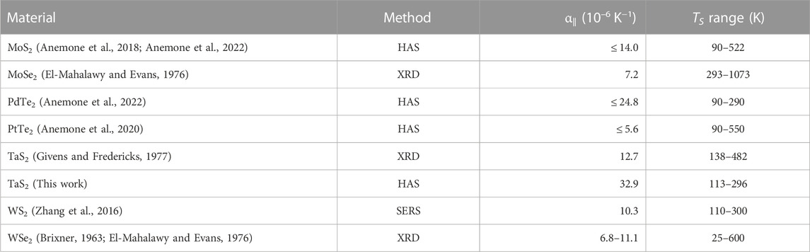
TABLE 1. Overview of the in-plane thermal expansion coefficients (TEC) of several TMdCs, how they were obtained and for which temperature range. In the case of a negligible TEC the upper limit is noted.
As every polarisable object in nature is subjected to the vdW force a fundamental understanding of the force is crucial for any quantitative description and theoretical treatment of molecular adsorption or surface reaction processes and is also of paramount importance for a better design and control of nanoscale devices. Beyond the applications of weak interactions in devices and materials, there are several experimental techniques analyzing nano-structured materials or explicitly using effects occurring from these weak interactions including atomic force microscopy and matter-wave scattering experiments which are probing dispersion forces (Fiedler et al., 2023).
However, in the case of topological nontrivial materials, HAS is the only experimental technique used to date to provide experimental information about the vdW interaction with a topological insulator (Tamtögl et al., 2021b). The latter stresses the need for experimental measurements even more so as, e.g., it is expected that peculiar effects such as the topological magnetoelectric effect (Dziom et al., 2017) cause an unconventional contribution to the vdW potential (Martín-Ruiz and Urrutia, 2018). Before we illustrate the experimental determination of the atom-surface vdW potential of 1T-TaS2 we will first describe HAS measurements of the step-height distribution in the following.
The surfaces of layered materials such as 1T-TaS2 are not perfectly flat, rather they are characterized by steps and parallel terraces, e.g., due to defects and the sample preparation process. The step heights and distributions of such periodically modulated surfaces can be calculated and resolved from interference effects in HAS (Farías and Rieder, 1998; Mayrhofer-Reinhartshuber et al., 2013a). As a result of the combination of the He beam being scattered from different terraces, constructive and destructive interference occurs. In a so-called drift measurement, the specular intensity is monitored while the kinetic energy of the incident He beam is changed. In the experiment this can be achieved by changing the nozzle temperature. By modulating the kinetic energy, the phase shift Δϕ for the He beam emerging from different terraces is varied. For the specific case of ϑi = ϑf (specular peak) the phase difference of two adjacent terrace levels is given by (Mayrhofer-Reinhartshuber et al., 2013a)
where h is step height and Δkz is the change of the wave vector component perpendicular to the surface. For constructive interference, the condition of in-phase scattering Δϕ = 2πn with an integer value of n must be fulfilled, whereas a half-integer value n leads to destructive interference due to anti-phase scattering. As a result, maxima and minima can be observed in the drift spectrum Figure 4A, where the normalized specular intensity is plotted against the incident wave vector ki. The measured specular intensity as a function of incident wave vector ki upon varying the nozzle temperature is plotted for the sample aligned along
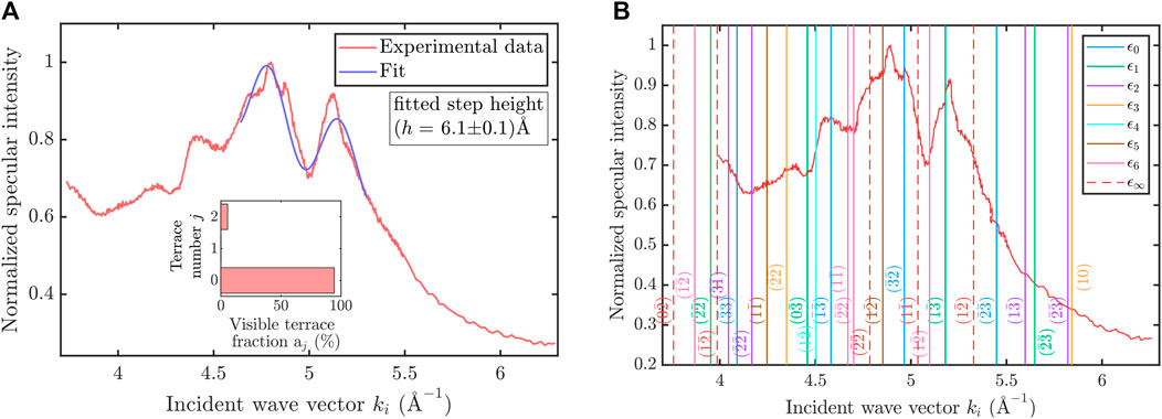
FIGURE 4. (A) Periodic oscillations in the measured specular intensity versus incident wave vector ki provide a measure for the step height distribution of the 1T-TaS2(0001) sample. Following an analysis upon fitting Eq. 6 (blue curve) to the experimental data points (red) we obtain a step height h = (6.1±0.1) Å for the measurement performed along the
As the incident wave vector ki is varied by changing the nozzle temperature TN, the He beam intensity scales via
Following a simple theoretical model to describe the periodic intensity modulation which assumes a coherent overlap of plane waves, emerging from different terrace levels, the specular intensity can be calculated with (Tölkes et al., 1997; Mayrhofer-Reinhartshuber et al., 2013a)
In Equation 6, I0 is the intensity for a flat surface without steps, φ(ki) the phase shift (see Eq. 5) and aj the visible fraction of the terrace level j. Eq. 6 has been fitted to the measured drift spectrum in the wave vector range 4.54 Å−1 < ki < 5.41 Å−1 and the best fit result is shown in Figure 4 as a blue line with the inset indicating the distribution of the visible terrace fractions. We obtain a surface step height of h = (6.1 ± 0.1) Å, which is in excellent agreement with the distance between two adjacent TaS2 layers (Bovet et al., 2003; Li et al., 2019; Kahraman et al., 2020).
As mentioned above, HAS provides direct experimental information about the vdW interaction between an atom and the surface and thus invaluable details about London dispersion forces of vdW layered materials. As a first step to determine the three-dimensional corrugated atom-surface interaction potential of 1T-TaS2, we follow a further analysis of the drift spectrum. The simple model for interference effects from steps (see Eq. 6) neglects the occurrence of selective adsorption resonances (SARs). These phenomena occur when an incoming helium atom is bound temporarily on the surface due to the attraction of the He-surface interaction potential. A SAR follows from the kinetic condition that the energy of the incident energy Ei equals the kinetic energy of the atom on the surface plus the binding energy ϵn of the potential:
Such adsorption processes give rise to peaks and dips in the drift spectrum (Tamtögl et al., 2021b). Therefore, these peaks and dips can be used to obtain the bound state energies of the potential. As a first step we concentrate on the laterally averaged atom-surface potential. Each peak/dip at a specific incident wave vector ki can be associated with a certain bound state energy ϵn and reciprocal lattice vector G pair which fulfills the condition given in Eq. (7). In the so-called free atom approximation, ϵn (Ki, G) is independent of Ki and G (Ruckhofer et al., 2019; Tamtögl et al., 2021b) and thus Figure 4B provides a direct measure of the bound state energies ϵn of the laterally averaged potential.
As a next step, we will then model the three-dimensional He-surface interaction potential, whereupon we use the corrugated Morse potential (CMP) due to its algebraic simplicity (Tamtögl et al., 2021b). It consists of two exponentials considering the repulsive and the attractive part of the potential as a function of the lateral position R on the surface and the distance z from the surface in the following form:
Here, κ is the stiffness and D the well depth of the potential, ξ(R) the corrugation function, which reflects the periodicity of the crystal surface, and ν0 is the surface average over e2κξ(R). The laterally averaged surface potential (i.e., without corrugation in the exponential) of Eq. 8 can be described analytically and the bound state energies are given by
with n being a positive integer,
The resulting bound state energies and their uncertainties are displayed in Table 2 while in Figure 5A a plot of the laterally averaged potential is shown. The positions of the corresponding SARs in the drift spectrum are displayed as vertical lines in Figure 4B, where each color belongs to one specific bound state energy ϵn and the red dashed lines illustrate the threshold energies. The labels next to the lines denote the corresponding reciprocal lattice vector G. For completeness, it should be mentioned that two more analytical bound state energies ϵ7 and ϵ8 exist, but they are quite close to zero, that is, to the threshold condition and therefore not displayed in Figure 4B and Table 2. In Figure 5A, the horizontal colored lines represent the first seven analytically calculated bound state energies. We note that SAR measurements are typically obtained with a cooled sample since with increasing temperature inelastic channels give rise to a broadening of the linewidth and may also cause changes from maxima to minima and vice versa (Tamtögl et al., 2018; Tamtögl et al., 2021b). Here we use measurements taken at room temperature as the position of the resonances becomes clearer at that temperature. It may be a consequence of the different phases of the cooled sample and the increased likelihood of rest gas adsorption for the latter.
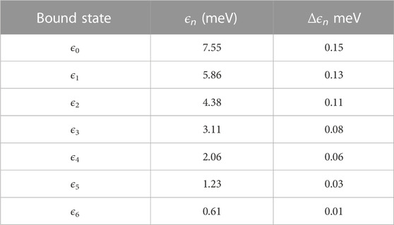
TABLE 2. Experimentally determined bound state energies ϵn for 1T-TaS2 and corresponding uncertainties upon fitting a laterally averaged Morse potential (Eq. 9) with D = 8.40 meV and κ = 0.45 Å−1.
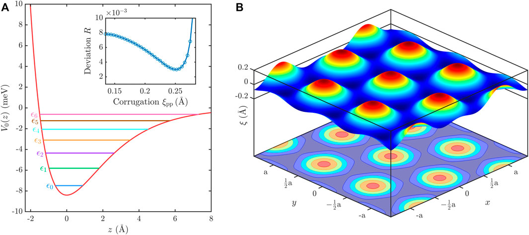
FIGURE 5. (A) Laterally averaged Morse potential for He-TaS2 with D = 8.40 meV and κ =0.45 Å−1 with the first 7 bound state energies ϵn. The inset shows the deviation R (Eq. 11) between CC-calculations and the experimental intensities upon varying the corrugation ξpp with a clear minimum at ξpp = 0.25 Å. (B) Shows a combined three-dimensional and contour plot of the obtained surface electronic corrugation ξ(x, y) as part of the three-dimensional corrugated Morse potential.
Our value of D is slightly smaller than the value D = 8.7 meV from Brusdeylins et al. whose value is based on intensity calculations (Brusdeylins et al., 1989) following the hard corrugated wall model together with the Beeby correction and thus does not directly consider scattering from a soft potential resulting in less accuracy compared to the elastic close-coupling method used in the previous works (Sanz and Miret-Artés, 2007; Mayrhofer-Reinhartshuber et al., 2013b). In general compared to other semiconductors, metals, and semimetals, 1T-TaS2 exhibits one of the “deepest” atom-surface interaction potentials, only surpassed by the graphene/graphite potential (Benedek and Toennies, 2018). At the same time, the stiffness κ is quite close to the value found for the topological insulator Bi2Se3 (Ruckhofer et al., 2019; Tamtögl et al., 2021b). With the outermost layer for Bi2Se3 being Se, located in the same column of the periodic table just below sulphur, it seems reasonable that the He−TaS2 potential exhibits a similar stiffness and supports a similar number of bound states.
Following the results of the laterally averaged atom-surface interaction potential we continue with the determination of the three-dimensional atom-surface interaction potential and the corresponding surface electronic corrugation (Tamtögl et al., 2021b; Allison et al., 2022). Following the CMP (Eq. 8), the corrugation ξ(R) for a hexagonal surface such as 1T-TaS2, can be described by a two-parameter Fourier ansatz,
where x and y depict the coordinates in the surface plane and ξ0 determines the corrugation amplitude. The ansatz above is based on the sixfold symmetry of the topmost surface layer. As the He beam provides an average of the long-range order, we omit the star of David clusters in this description. The corrugation is then typically expressed in terms of the peak-to-peak value ξpp = max(ξ) − min(ξ). With the CMP (Eq. 8) we are able to calculate the diffraction intensities and compare those with the experimentally measured ones to obtain a value for the peak-to-peak corrugation ξpp.
A theoretical framework to describe the elastic scattering of He atoms from surfaces is the close-coupling (CC) formalism, which is more exact than the hard-wall approximation, but still computationally manageable (Sanz and Miret-Artés, 2007; Allison et al., 2022). The starting point here is the time-independent Schrödinger equation together with the CMP, which contains the Fourier series expansion (Eq. 10) in the exponentials, yielding a set of coupled differential equations for the diffracted waves. These equations are solved for using the CC algorithm, taking into account all open channels and 110 closed channels. The z − boundaries of the integration were set to [−6, 18]. A detailed theoretical treatment and the corresponding equations can be found in several references (Miret-Artés, 1995; Sanz and Miret-Artés, 2007; Mayrhofer-Reinhartshuber et al., 2013b; Kraus et al., 2015), while an implementation of the CC algorithm is available from https://repository.tugraz.at/records/cd0y0-xa478 under the GNU General Public License v3.0.
By comparing the elastic diffraction intensities calculated with the close-coupling algorithm we are able to determine the corrugation of the sample surface (Ruckhofer et al., 2019; Schmutzler et al., 2022). For the measured diffraction intensities we used the peak areas instead of the peak height to account for broadening due to the energy spread of the He atoms, angular resolution of the apparatus, and size effects of the crystal surface (Ruckhofer et al., 2019). For the CC calculations, the intensities have been corrected by the Debye-Waller factor, and the values for D and κ from above were kept constant, while the corrugation amplitude ξ0 (see Eq. 10) was varied between 0.05 and 0.90 Å−1. The best corrugation value ξ0 is the one that minimises the deviation R between simulated and experimentally obtained diffraction intensities
with N the number of experimentally measured diffraction scans. As for the calculation of the lattice constants we used in total 22 scans at various incident energies for the optimization process of Eq. 11 to find a global minimum of R as a function of ξ0. It results in a surface electronic peak-to-peak corrugation (see inset of Figure 5A) of
which corresponds to 7.5% of the surface lattice constant a. Figure 5B shows a plot of the best-fit surface electronic corrugation according to Equation 10.
So far, there barely exist any other HAS studies of other TMdCs that determine the electronic corrugation. Anemone et al. studied the 1T-PtTe2 surface and provided a rough estimation of the maximum corrugation amplitude with 0.33 Å (Anemone et al., 2020). It should be mentioned that their estimation is based on the HCW model, which makes a direct comparison difficult. Similarly, various low-index metal surfaces have been studied in atomic beam scattering experiments and revealed a significantly smaller corrugation (Benedek and Toennies, 2018). On the other hand, in comparison to the binary topological insulators and single-element semimetals, which have been studied recently with HAS (Tamtögl et al., 2021b) and analyzed in a similar manner, TaS2 exhibits a similar surface electronic corrugation.
The increasing interest in vdW 2D materials makes 1T-TaS2 probably one of the best-studied TMdCs and, in fact, 1T-TaS2 has already been investigated by HAS over 40 years ago. However, these studies were concentrated on a few limited aspects of the system, and theoretical descriptions at that time relied on simplistic models. In contrast, we have reported a detailed helium atom scattering study of the archetypal charge-density wave system and transition metal dichalcogenide 1T-TaS2. The electron-phonon coupling has been compared with measurements of the 3D topological insulator TlBiTe2. The electron-phonon coupling λ in the C-CDW phase of 1T-TaS2 has been determined with λ = 0.59 ± 0.12 for 1T-TaS2 and is thus much larger than the value for TlBiTe2 (λ = 0.09 ± 0.01) which is similar to other semimetal and topological insulator surfaces. In fact, since λ of TlBiTe2 is so close to λ found for Bi2Te2Se we conclude that the existence of the Dirac cone alone, as found for both TIs, does not give rise to a significant e-ph coupling.
The large λ of 1T-TaS2 on the other hand, may be a consequence both of the CDW phase as well as the weak bonding between the individual dichalcogenide layers. The much stronger inter-layer bonding of TlBiTe2 on the other hand, is reflected in the difficulty to cleave the crystals resulting in a very rough surface with a domain size of about 20 nm and overall comparably small scattering intensities. It would also be interesting to establish whether other TMdCs with a vdW layered structure such as 1T-TaS2 but different bonding between the dichalcogenide layers exhibit a different λ in accordance to the dependence of λ on the substrate bonding for metal-supported graphene where λ varies between 0.06 and 0.22 (Benedek et al., 2021).
By means of elastic scattering, the structural properties of 1T-TaS2 have been studied and a linear in-plane thermal expansion coefficient with α‖ = (33 ± 12) ⋅ 10–6 K−1 has been determined, which is larger than the value from X-ray diffraction and comparable to other TMdCs (Givens and Fredericks, 1977; Anemone et al., 2022). Interference and resonance effects which can be observed upon varying the He beam energy provide further information allowing us to determine the step-height between parallel terraces with h = (6.1 ± 0.1) Å in accordance with the spacing between the dichalcogenide layers. Based on the mentioned interference effects we are able to determine the three-dimensional atom-surface interaction potential of 1T-TaS2. Using a corrugated Morse potential, the laterally averaged potential is best described by a well depth D = (8.40 ± 0.15) meV and a stiffness κ = (0.45 ± 0.02) Å−1. Hence 1T-TaS2 exhibits one of the “deepest” atom-surface interaction potentials compared to other semiconductors/(semi)metals, only surpassed by graphene/graphite which may again be an indication of the “pure” vdW nature of the interlayer bonding. The full three-dimensional potential follows then from a comparison of the diffraction intensities with quantum-mechanical scattering calculations. The optimal agreement is achieved for a surface electronic corrugation with a peak-to-peak value of ξpp = 0.25 Å. While the value is larger than for low-index metal surfaces it is comparable to other semiconductor/semimetal surfaces.
The raw data supporting the conclusions of this article will be made available by the authors, without undue reservation.
AT provided the experimental concept and MB synthesized the samples and performed additional sample characterization. PM and AR were responsible for the experimental setup and performed the measurements. Data analysis, visualization, and discussion were done by PM, NH, and AT. The manuscript was written by PM and AT. All authors contributed to the article and approved the submitted version.
This research was funded in whole, or in part, by the Austrian Science Fund (FWF) [P34704] and NAWI Graz. For the purpose of open access, the author has applied a CC BY public copyright license to any Author Accepted Manuscript version arising from this submission. MB acknowledges financial support from the Independent Research Fund Denmark’s Sapere Aude program (Grant No. 7027-00077A).
We would like to thank G. Benedek, W. E. Ernst, and M. Pusterhofer for their helpful discussions. We would like to thank S. Chandra and C. Felser for providing us with a TlBiTe2 sample.
The authors declare that the research was conducted in the absence of any commercial or financial relationships that could be construed as a potential conflict of interest.
All claims expressed in this article are solely those of the authors and do not necessarily represent those of their affiliated organizations, or those of the publisher, the editors and the reviewers. Any product that may be evaluated in this article, or claim that may be made by its manufacturer, is not guaranteed or endorsed by the publisher.
1m⋆ = 0.086 me, ϵr = 56.15 and nc = 2·1019 cm−3
Al-Makeen, M. M., Guo, X., Wang, Y., Yang, D., You, S., Yassine, M., et al. (2022). Investigation of the electron–phonon coupling in Dirac semimetal PdTe2 via temperature-dependent Raman spectroscopy. Phys. Status Solidi RRL 16, 2200257. doi:10.1002/pssr.202200257
Allison, W., Miret-Artés, S., and Pollak, E. (2022). Perturbation theory of scattering for grazing-incidence fast-atom diffraction. Phys. Chem. Chem. Phys. 24, 15851–15859. doi:10.1039/D2CP01013E
Anemone, G., Al Taleb, A., Castellanos-Gomez, A., and Farías, D. (2018). Experimental determination of thermal expansion of natural MoS2. 2D Mater 5, 035015. doi:10.1088/2053-1583/aabe4a
Anemone, G., Garnica, M., Zappia, M., Aguilar, P. C., Al Taleb, A., Kuo, C.-N., et al. (2020). Experimental determination of surface thermal expansion and electron–phonon coupling constant of 1T-PtTe2. 2D Mater 7, 025007. doi:10.1088/2053-1583/ab6268
Anemone, G., Taleb, A. A., Politano, A., Kuo, C.-N., Lue, C. S., Miranda, R., et al. (2022). Setting the limit for the lateral thermal expansion of layered crystals via helium atom scattering. Phys. Chem. Chem. Phys. 24, 13229–13233. doi:10.1039/d2cp00758d
Bao, J., Yang, L., and Wang, D. (2022). Influence of torsional deformation on the electronic structure and optical properties of 1T-TaS2 monolayer. J. Mol. Struct. 1258, 132667. doi:10.1016/j.molstruc.2022.132667
Benedek, G., Manson, J. R., and Miret-Artés, S. (2020a). The electron-phonon interaction of low-dimensional and multi-dimensional materials from he atom scattering. Adv. Mat. 32, 2002072. doi:10.1002/adma.202002072
Benedek, G., Manson, J. R., and Miret-Artés, S. (2021). The electron-phonon coupling constant for single-layer graphene on metal substrates determined from He atom scattering. Phys. Chem. Chem. Phys. 23, 7575–7585. doi:10.1039/D0CP04729E
Benedek, G., Manson, J. R., Miret-Artés, S., Ruckhofer, A., Ernst, W. E., Tamtögl, A., et al. (2020b). Measuring the electron–phonon interaction in two-dimensional superconductors with He-atom scattering. Condens. Matter 5, 79. doi:10.3390/condmat5040079
Benedek, G., Miret-Artés, S., Manson, J. R., Ruckhofer, A., Ernst, W. E., and Tamtögl, A. (2020c). Origin of the electron-phonon interaction of topological semimetal surfaces measured with helium atom scattering. J. Phys. Chem. Lett. 11, 1927–1933. doi:10.1021/acs.jpclett.9b03829
Benedek, G., Miret-Artés, S. S., Toennies, J. P., and Manson, J. R. (2018). Electron–phonon coupling constant of metallic overlayers from specular He atom scattering. J. Phys. Chem. Lett. 9, 76–83. doi:10.1021/acs.jpclett.7b03047
Benedek, G., and Toennies, J. P. (2018). Atomic scale dynamics at surfaces. Berlin, Heidelberg: Springer Berlin Heidelberg. doi:10.1007/978-3-662-56443-1
Bovet, M., van Smaalen, S., Berger, H., Gaal, R., Forró, L., Schlapbach, L., et al. (2003). Interplane coupling in the quasi-two-dimensional 1T−TaS2. Phys. Rev. B 67, 125105. doi:10.1103/PhysRevB.67.125105
Brixner, L. H. (1963). X-Ray study and thermoelectric properties of the WxT11−xSe2 system. J. Electrochem. Soc. 110, 289. doi:10.1149/1.2425734
Brusdeylins, G., Heimlich, C., and Toennies, J. (1989). Helium scattering from the layered compound single crystal surface of 1T-TaS2 in the temperature region of charge density wave reconstruction. Surf. Sci. 211-212, 98–105. doi:10.1016/0039-6028(89)90758-9
Cantini, P., Boato, G., and Colella, R. (1980). Surface charge density waves observed by atomic beam diffraction. Phys. B+C 99, 59–63. doi:10.1016/0378-4363(80)90211-9
Chen, Y. L., Liu, Z. K., Analytis, J. G., Chu, J. H., Zhang, H. J., Yan, B. H., et al. (2010). Single Dirac cone topological surface state and unusual thermoelectric property of compounds from a new topological insulator family. Phys. Rev. Lett. 105, 266401. doi:10.1103/PhysRevLett.105.266401
Choe, J., Lujan, D., Rodriguez-Vega, M., Ye, Z., Leonardo, A., Quan, J., et al. (2021). Electron-phonon and spin-lattice coupling in atomically thin layers of MnBi2Te4. Nano Lett. 21, 6139–6145. doi:10.1021/acs.nanolett.1c01719
Clerc, F., Battaglia, C., Bovet, M., Despont, L., Monney, C., Cercellier, H., et al. (2006). Lattice-distortion-enhanced electron-phonon coupling and Fermi surface nesting in 1T-TaS2. Phys. Rev. B 74, 155114. doi:10.1103/PhysRevB.74.155114
Coleman, R. V., McNairy, W. W., and Slough, C. G. (1992). Amplitude modulation of charge-density-wave domains in 1T-TaS2 at 300 K. Phys. Rev. B 45, 1428–1431. doi:10.1103/PhysRevB.45.1428
Duong, D. L., Yun, S. J., and Lee, Y. H. (2017). van der Waals layered materials: opportunities and challenges. ACS Nano 11, 11803–11830. doi:10.1021/acsnano.7b07436
Dziom, V., Shuvaev, A., Pimenov, A., Astakhov, G. V., Ames, C., Bendias, K., et al. (2017). Observation of the universal magnetoelectric effect in a 3D topological insulator. Nat. Commun. 8, 15197. doi:10.1038/ncomms15197
El-Mahalawy, S. H., and Evans, B. L. (1976). The thermal expansion of 2H -MoS2, 2H-MoSe2 and 2H -WSe2 between 20 and 800°C. J. Appl. Crystallogr. 9, 403–406. doi:10.1107/S0021889876011709
Eremeev, S. V., Bihlmayer, G., Vergniory, M., Koroteev, Y. M., Menshchikova, T. V., Henk, J., et al. (2011). Ab initio electronic structure of thallium-based topological insulators. Phys. Rev. B 83, 205129. doi:10.1103/PhysRevB.83.205129
Eremeev, S. V., Koroteev, Y. M., and Chulkov, E. V. (2010). Ternary thallium-based semimetal chalcogenides tl-v-vi2 as a new class of three-dimensional topological insulators. JETP Lett. 91, 594–598. doi:10.1134/S0021364010110111
Farías, D., and Rieder, K.-H. (1998). Atomic beam diffraction from solid surfaces. Rep. Prog. Phys. 61, 1575–1664. doi:10.1088/0034-4885/61/12/001
Fiedler, J., Berland, K., Borchert, J. W., Corkery, R. W., Eisfeld, A., Gelbwaser-Klimovsky, D., et al. (2023). Perspectives on weak interactions in complex materials at different length scales. Phys. Chem. Chem. Phys. 25, 2671–2705. doi:10.1039/D2CP03349F
Givens, F. L., and Fredericks, G. E. (1977). Thermal expansion op NbSe2 and TaS2. J. Phys. Chem. Solids 38, 1363–1365. doi:10.1016/0022-3697(77)90008-7
Han, S., Tang, Q., Yuan, H., Luo, Y., and Liu, H. (2023). Effects of electron-phonon coupling on the phonon transport properties of the Weyl semimetals NbAs and TaAs: a comparative study. J. Materiomics 9, 520–526. doi:10.1016/j.jmat.2022.12.001
Hein, R. A., and Swiggard, E. M. (1970). Superconductivity in TlBiTe2: a low carrier density (III-V)VI2 compound. Phys. Rev. Lett. 24, 53–55. doi:10.1103/PhysRevLett.24.53
Johannes, M. D., and Mazin, I. I. (2008). Fermi surface nesting and the origin of charge density waves in metals. Phys. Rev. B 77, 165135. doi:10.1103/PhysRevB.77.165135
Kahraman, Z., Yagmurcukardes, M., and Sahin, H. (2020). Functionalization of single-layer TaS2 and formation of ultrathin Janus structures. J. Mater. Res. 35, 1397–1406. doi:10.1557/jmr.2020.64
Klanjšek, M., Zorko, A., Žitko, R., Mravlje, J., Jagličić, Z., Biswas, P. K., et al. (2017). A high-temperature quantum spin liquid with polaron spins. Nat. Phys. 13, 1130–1134. doi:10.1038/nphys4212
Kratochvilova, M., Hillier, A. D., Wildes, A. R., Wang, L., Cheong, S.-W., and Park, J.-G. (2017). The low-temperature highly correlated quantum phase in the charge-density-wave 1T-TaS2 compound. npj Quantum Mater 2, 42. doi:10.1038/s41535-017-0048-1
Kraus, P., Tamtögl, A., Mayrhofer-Reinhartshuber, F., Apolloner, M., Gösweiner, C., Miret-Artés, S., et al. (2015). Surface structure of Bi(111) from helium atom scattering measurements. Inelastic close-coupling formalism. J. Phys. Chem. C 119, 17235–17242. doi:10.1021/acs.jpcc.5b05010
Kumar, A., Kumar, S., Miyai, Y., and Shimada, K. (2022). Temperature-dependent band modification and energy dependence of the electron-phonon interaction in the topological surface state on Bi2Te3. Phys. Rev. B 106, L121104. doi:10.1103/PhysRevB.106.L121104
Kuroda, K., Ye, M., Kimura, A., Eremeev, S. V., Krasovskii, E. E., Chulkov, E. V., et al. (2010). Experimental realization of a three-dimensional topological insulator phase in ternary chalcogenide tlbise2. Phys. Rev. Lett. 105, 146801. doi:10.1103/PhysRevLett.105.146801
Kuroda, K., Ye, M., Schwier, E. F., Nurmamat, M., Shirai, K., Nakatake, M., et al. (2013). Experimental verification of the surface termination in the topological insulator TlBiSe2 using core-level photoelectron spectroscopy and scanning tunneling microscopy. Phys. Rev. B 88, 245308. doi:10.1103/PhysRevB.88.245308
Kurosaki, K., Kosuga, A., and Yamanaka, S. (2003). Thermoelectric properties of TlBiTe2. J. Alloys Compd. 351, 279–282. doi:10.1016/S0925-8388(02)01038-1
Lai, J.-M., Xie, Y.-R., and Zhang, J. (2021). Detection of electron-phonon coupling in two-dimensional materials by light scattering. Nano Res. 14, 1711–1733. doi:10.1007/s12274-020-2943-1
Law, K. T., and Lee, P. A. (2017). 1T-TaS2 as a quantum spin liquid. Proc. Natl. Acad. Sci. 114, 6996–7000. doi:10.1073/pnas.1706769114
Li, Y., Xia, Y., Ekahana, S. A., Kumar, N., Jiang, J., Yang, L., et al. (2017). Topological origin of the type-ii Dirac fermions in PtSe2. Phys. Rev. Mat. 1, 074202. doi:10.1103/PhysRevMaterials.1.074202
Li, Y., Xiao, H., Zhou, P., and Cao, J. (2019). Electronic structures of twist-stacked 1T-TaS2 bilayers. Phys. Lett. A 383, 2302–2308. doi:10.1016/j.physleta.2019.04.043
Lin, H., Markiewicz, R. S., Wray, L. A., Fu, L., Hasan, M. Z., and Bansil, A. (2010). Single-Dirac-Cone topological surface states in the TlBiSe2 class of topological semiconductors. Phys. Rev. Lett. 105, 036404. doi:10.1103/PhysRevLett.105.036404
Liu, Y., Weiss, N. O., Duan, X., Cheng, H.-C., Huang, Y., and Duan, X. (2016). Van der Waals heterostructures and devices. Nat. Rev. Mater 1, 16042. doi:10.1038/natrevmats.2016.42
Lubell, M., and Mazelsky, R. (1965). Thermoelectric properties of the system gete-tlbite2. Solid-State Electron 8, 729–733. doi:10.1016/0038-1101(65)90060-2
Manson, J., Benedek, G., and Miret-Artés, S. (2022). Atom scattering as a probe of the surface electron-phonon interaction at conducting surfaces. Surf. Sci. Rep. 77, 100552. doi:10.1016/j.surfrep.2022.100552
Martín-Ruiz, A., and Urrutia, L. F. (2018). Interaction of a hydrogenlike ion with a planar topological insulator. Phys. Rev. A 97, 022502. doi:10.1103/PhysRevA.97.022502
Mayrhofer-Reinhartshuber, M., Tamtögl, A., Kraus, P., and Ernst, W. E. (2013a). Helium atom scattering investigation of the Sb(111) surface. J. Phys.: Condens. Matter 25, 395002. doi:10.1088/0953-8984/25/39/395002
Mayrhofer-Reinhartshuber, M., Kraus, P., Tamtögl, A., Miret-Artés, S., and Ernst, W. E. (2013b). Helium-surface interaction potential of Sb(111) from scattering experiments and close-coupling calculations. Phys. Rev. 88, 205425. doi:10.1103/PhysRevB.88.205425
Miret-Artés, S. (1995). Resonant inelastic scattering of atoms from surfaces. Surf. Sci. 339, 205–220. doi:10.1016/0039-6028(95)00632-x
National Institute of Standards and Technology (2018). Innovation unleashed. Maryland, United States: National Institute of Standards and Technology.
Ngankeu, A. S., Mahatha, S. K., Guilloy, K., Bianchi, M., Sanders, C. E., Hanff, K., et al. (2017). Quasi-one-dimensional metallic band dispersion in the commensurate charge density wave of 1T-TaS2. Phys. Rev. B 96, 195147. doi:10.1103/PhysRevB.96.195147
Osterhoudt, G. B., Wang, Y., Garcia, C. A. C., Plisson, V. M., Gooth, J., Felser, C., et al. (2021). Evidence for dominant phonon-electron scattering in weyl semimetal WP2. Phys. Rev. X 11, 011017. doi:10.1103/PhysRevX.11.011017
Paraskevopoulos, K. M. (1985). Electron effective mass dependence on carrier concentration in TlBiTe2 monocrystals. Phys. Status Solidi B 127, K45–K50. doi:10.1002/pssb.2221270156
Pei, C., Huang, P., Zhu, P., Liu, L., Wang, Q., Zhao, Y., et al. (2022). Pressure-induced superconductivity extending across the topological phase transition in thallium-based topological materials. Cell Rep. Phys. Sci. 3, 101094. doi:10.1016/j.xcrp.2022.101094
Pielmeier, F., Landolt, G., Slomski, B., Muff, S., Berwanger, J., Eich, A., et al. (2015). Response of the topological surface state to surface disorder in tlbise 2. New J. Phys. 17, 023067. doi:10.1088/1367-2630/17/2/023067
Popovich, N., Shura, V., Diakonov, V., Fita, I., and Levchenko, G. (1984). On the superconductivity in TlBiTe2. Solid State Commun. 50, 979–981. doi:10.1016/0038-1098(84)90269-2
Rossnagel, K. (2011). On the origin of charge-density waves in select layered transition-metal dichalcogenides. J. Phys. Condens. Matter 23, 213001. doi:10.1088/0953-8984/23/21/213001
Ruckhofer, A., Campi, D., Bremholm, M., Hofmann, P., Benedek, G., Bernasconi, M., et al. (2020). Terahertz surface modes and electron-phonon coupling on Bi2Se3(111). Phys. Rev. Res. 2, 023186. doi:10.1103/PhysRevResearch.2.023186
Ruckhofer, A., Tamtögl, A., Pusterhofer, M., Bremholm, M., and Ernst, W. E. (2019). Helium-surface interaction and electronic corrugation of Bi2Se3(111). J. Phys. Chem. C 123, 17829–17841. doi:10.1021/acs.jpcc.9b03450
Ruckhofer, A., Benedek, G., Bremholm, M., Ernst, W. E., and Tamtögl, A. (2023). Observation of Dirac charge-density waves in Bi2Te2Se. Nanomaterials 13, 476. doi:10.3390/nano13030476
Sanders, C. E., Dendzik, M., Ngankeu, A. S., Eich, A., Bruix, A., Bianchi, M., et al. (2016). Crystalline and electronic structure of single-layer TaS2. Phys. Rev. B 94, 081404. doi:10.1103/PhysRevB.94.081404
Sanz, A. S., and Miret-Artés, S. (2007). Selective adsorption resonances: quantum and stochastic approaches. Phys. Rep. 451, 37–154. doi:10.1016/j.physrep.2007.08.001
Schmutzler, S. J., Ruckhofer, A., Ernst, W. E., and Tamtögl, A. (2022). Surface electronic corrugation of a one-dimensional topological metal: Bi(114). Phys. Chem. Chem. Phys. 24, 9146–9155. doi:10.1039/D1CP05284E
Shimada, T., Ohuchi, F., and Parkinson, B. (1994). Work function and photothreshold of layered metal dichalcogenides. Jpn. J. Appl. Phys. 33, 2696. doi:10.1143/jjap.33.2696
Shojaei, I. A., Pournia, S., Le, C., Ortiz, B. R., Jnawali, G., Zhang, F.-C., et al. (2021). A Raman probe of phonons and electron-phonon interactions in the Weyl semimetal NbIrTe4. Sci. Rep. 11, 8155. doi:10.1038/s41598-021-87302-y
Singh, B., Lin, H., Prasad, R., and Bansil, A. (2016). Role of surface termination in realizing well-isolated topological surface states within the bulk band gap in TlBiSe2 and TlBiTe2. Phys. Rev. B 93, 085113. doi:10.1103/PhysRevB.93.085113
Singh, B., Sharma, A., Lin, H., Hasan, M. Z., Prasad, R., and Bansil, A. (2012). Topological electronic structure and weyl semimetal in the tlbise2 class of semiconductors. Phys. Rev. B 86, 115208. doi:10.1103/PhysRevB.86.115208
Sobota, J. A., Teitelbaum, S. W., Huang, Y., Querales-Flores, J. D., Power, R., Allen, M., et al. (2023). Influence of local symmetry on lattice dynamics coupled to topological surface states. Phys. Rev. B 107, 014305. doi:10.1103/PhysRevB.107.014305
Spitzer, D. P., and Sykes, J. A. (1966). The Tl2Te3-Bi2Te3 system. J. Appl. Phys. 37, 1563–1566. doi:10.1063/1.1708568
Tamtögl, A., Bahn, E., Sacchi, M., Zhu, J., Ward, D. J., Jardine, A. P., et al. (2021a). Motion of water monomers reveals a kinetic barrier to ice nucleation on graphene. Nat. Commun. 12, 3120. doi:10.1038/s41467-021-23226-5
Tamtögl, A., Carter, E. A., Ward, D. J., Avidor, N., Kole, P. R., Jardine, A. P., et al. (2016). Note: a simple sample transfer alignment for ultra-high vacuum systems. Rev. Sci. Instrum. 87, 066108. doi:10.1063/1.4954728
Tamtögl, A., Kraus, P., Avidor, N., Bremholm, M., Hedegaard, E. M. J., Iversen, B. B., et al. (2017). Electron-phonon coupling and surface Debye temperature of Bi2Te3(111) from helium atom scattering. Phys. Rev. B 95, 195401. doi:10.1103/PhysRevB.95.195401
Tamtögl, A., Kraus, P., Mayrhofer-Reinhartshuber, M., Benedek, G., Bernasconi, M., Dragoni, D., et al. (2019). Statics and dynamics of multivalley charge density waves in Sb(111). npj Quantum Mater 4, 28. doi:10.1038/s41535-019-0168-x
Tamtögl, A., Mayrhofer-Reinhartshuber, M., Balak, N., Ernst, W. E., and Rieder, K. (2010). Elastic and inelastic scattering of He atoms from Bi(111). J. Phys. Condens. Matter 22, 304019. doi:10.1088/0953-8984/22/30/304019
Tamtögl, A., Pusterhofer, M., Bremholm, M., Hedegaard, E. M., Iversen, B. B., Hofmann, P., et al. (2018). A helium-surface interaction potential of Bi2Te3(111) from ultrahigh-resolution spin-echo measurements. Surf. Sci. 678, 25–31. doi:10.1016/j.susc.2018.02.006
Tamtögl, A., Ruckhofer, A., Campi, D., Bremholm, M., Ernst, W. E., Hofmann, P., et al. (2021b). Atom-surface van der Waals potentials of topological insulators and semimetals from scattering measurements. Phys. Chem. Chem. Phys. 23, 7637–7652. doi:10.1039/D0CP05388K
Tölkes, C., Zeppenfeld, P., Krzyzowski, M. A., David, R., and Comsa, G. (1997). Preparation of well-ordered cobalt nanostructures on Au(111). Phys. Rev. B 55, 13932–13937. doi:10.1103/physrevb.55.13932
Tsen, A. W., Hovden, R., Wang, D., Kim, Y. D., Okamoto, J., Spoth, K. A., et al. (2015). Structure and control of charge density waves in two-dimensional 1T-TaS 2. Proc. Natl. Acad. Sci. 112, 15054–15059. doi:10.1073/pnas.1512092112
Vaskivskyi, I., Gospodaric, J., Brazovskii, S., Svetin, D., Sutar, P., Goreshnik, E., et al. (2015). Controlling the metal-to-insulator relaxation of the metastable hidden quantum state in 1T-TaS2. Sci. Adv. 1, e1500168. doi:10.1126/sciadv.1500168
Wang, Y. D., Yao, W. L., Xin, Z. M., Han, T. T., Wang, Z. G., Chen, L., et al. (2020). Band insulator to Mott insulator transition in 1T-TaS2. Nat. Commun. 11, 4215. doi:10.1038/s41467-020-18040-4
Wilson, J., Salvo, F. D., and Mahajan, S. (1975). Charge-density waves and superlattices in the metallic layered transition metal dichalcogenides. Adv. Phys. 24, 117–201. doi:10.1080/00018737500101391
Wilson, J. A., Salvo, F. J. D., and Mahajan, S. (2001). Charge-density waves and superlattices in the metallic layered transition metal dichalcogenides. Adv. Phys. 50, 1171–1248. doi:10.1080/00018730110102718
Xu, B., Dai, Y. M., Zhao, L. X., Wang, K., Yang, R., Zhang, W., et al. (2017). Temperature-tunable Fano resonance induced by strong coupling between Weyl fermions and phonons in TaAs. Nat. Commun. 8, 14933. doi:10.1038/ncomms14933
Yan, B., Liu, C.-X., Zhang, H.-J., Yam, C.-Y., Qi, X.-L., Frauenheim, T., et al. (2010). Theoretical prediction of topological insulators in thallium-based III-V-VI2 ternary chalcogenides. EPL Europhys. Lett. 90, 37002. doi:10.1209/0295-5075/90/37002
Yu, Y., Yang, F., Lu, X. F., Yan, Y. J., Cho, Y.-H., Ma, L., et al. (2015). Gate-tunable phase transitions in thin flakes of 1T-TaS2. Nat. Nanotechnol. 10, 270–276. doi:10.1038/nnano.2014.323
Zhang, D., Wu, Y.-C., Yang, M., Liu, X., Coileáin, C. Ó., Xu, H., et al. (2016). Probing thermal expansion coefficients of monolayers using surface enhanced Raman scattering. RSC Adv. 6, 99053–99059. doi:10.1039/C6RA20623A
Keywords: transition metal dichalcogenide, topological insulator, charge density wave, helium atom scattering, electron-phonon coupling, thermal expansion
Citation: Maier P, Hourigan NJ, Ruckhofer A, Bremholm M and Tamtögl A (2023) Surface properties of 1T-TaS2 and contrasting its electron-phonon coupling with TlBiTe2 from helium atom scattering. Front. Chem. 11:1249290. doi: 10.3389/fchem.2023.1249290
Received: 28 June 2023; Accepted: 19 October 2023;
Published: 16 November 2023.
Edited by:
Malgorzata Biczysko, Shanghai University, ChinaReviewed by:
Tie Yang, Southwest University, ChinaCopyright © 2023 Maier, Hourigan, Ruckhofer, Bremholm and Tamtögl. This is an open-access article distributed under the terms of the Creative Commons Attribution License (CC BY). The use, distribution or reproduction in other forums is permitted, provided the original author(s) and the copyright owner(s) are credited and that the original publication in this journal is cited, in accordance with accepted academic practice. No use, distribution or reproduction is permitted which does not comply with these terms.
*Correspondence: Philipp Maier, cGhpbGlwcC5tYWllckB0dWdyYXouYXQ=
Disclaimer: All claims expressed in this article are solely those of the authors and do not necessarily represent those of their affiliated organizations, or those of the publisher, the editors and the reviewers. Any product that may be evaluated in this article or claim that may be made by its manufacturer is not guaranteed or endorsed by the publisher.
Research integrity at Frontiers
Learn more about the work of our research integrity team to safeguard the quality of each article we publish.