 X. B. Yuan1
 Y. H. Guo
 J. F. Ren
95% of researchers rate our articles as excellent or good
Learn more about the work of our research integrity team to safeguard the quality of each article we publish.
Find out more
ORIGINAL RESEARCH article
Front. Chem. , 22 February 2022
Sec. Theoretical and Computational Chemistry
Volume 10 - 2022 | https://doi.org/10.3389/fchem.2022.861838
This article is part of the Research Topic Photocatalysis and Electrocatalysis for Energy Conversion View all 11 articles
In this work, we study the electronic structure, the effective mass, and the optical properties of the MoSSe/InS van der Waals heterostructures (vdWHs) by first-principles calculations. The results indicate that the MoSSe/InS vdWH is an indirect band gap semiconductor and has type-Ⅱ band alignment in which the electrons and holes located at the InS and the MoSSe side, respectively. The band edge position, the band gap and the optical absorption of the MoSSe/InS vdWH can be tuned when biaxial strains are applied. In addition, compared with MoSSe and InS monolayers, the optical absorption of the MoSSe/InS vdWH is improved both in the visible and the ultraviolet regions. These findings indicate that the MoSSe/InS vdWHs have potential applications in optoelectronic devices.
With the discovery of graphene in 2004, two-dimensional (2D) materials have been widely studied and applied due to their unique structures and excellent physical and chemical properties (Novoselov et al., 2004). In the past decades, a large number of 2D materials have been emerged, such as transition metal dichalcogenides (TMDCs) (Choi et al., 2017; Qiu et al., 2020), silicene (Fleurence et al., 2012; Wu et al., 2014), group-III monochalcogenides (Huang et al., 2019), Mxenes (Zhou et al., 2021), etc. In order to obtain high-performance devices, the advantages of a single layer 2D material are slightly insufficient, so the van der Waals heterostructures (vdWHs) formed by the van der Waals forces along the vertical superposition of two different 2D materials has been attracted widespread attention (Guo et al., 2021a; Zhao et al., 2021). A variety of vdWHs have been developed, which can be classified into three band alignments, i.e., straddling type-I, staggered type-II, and broken-gap type-III (Özçelik et al., 2016).
The vdWHs not only contain some of the advantages of the isolated monolayers but also produce some other properties (Ren et al., 2021a; Ren et al., 2021b; Ren et al., 2021c; Sun et al., 2022; Shen et al., 2022). For example, Liu et al. proposed the MoSSe/g-GeC heterostructure as a promising photovoltaic application material in which visible optical absorption and catalytic activity can be adjusted by strain engineering (Liu et al., 2021). M. M. Obeid and others revealed that GaSe/HfS2 heterostructures have high carrier mobility and can be converted from semiconductor to metal and from indirect band gap to direct band gap when the external electric field is strengthened (Obeid et al., 2020). Zhu et al. found that GaN/Zr2CO2 heterostructure has a promising application in tunable high-performance optoelectronic nanodevices due to its large conduction band offset (CBO) and tunable band gap (Zhu et al., 2021). Zhang et al. proved that P-GaSe/InS isomorphous heterostructure has excellent performance as a photocatalytic and water splitting material (Zhang et al., 2021).
On the other hand, after Janus MoSSe was successfully synthesized by chemical vapor deposition (CVD) method in 2017 (Lu et al., 2017; Zhang et al., 2017), the unique physical properties of 2D Janus TMDCs due to their mirror asymmetry have been attracted widespread attention. The Janus MoSSe has an easy-to-tune band gap, strong visible optical absorption and suitable band alignment (Yin et al., 2018); Mo atoms are located between S atoms and Se atoms, so an internal electric field is formed, which promotes electron-hole separation and inhibits exciton recombination (Chen et al., 2019). In addition, as a new type of 2D material, Group-III chalcogenides (MX, M = Ga and In, X = S, Se) have been attracted great attention in photoelectric devices due to their wide band gap, high electron mobility, good thermoelectric performance and optical responses (Miao et al., 2016; Xu et al., 2016; Hung et al., 2017). InS has been successfully synthesized experimentally and has a similar structure to InSe (Hollingsworth et al., 2000). Monolayer InS has good optical response characteristics and large band gap. However, InS has some disadvantages in visible optical absorption due to the large indirect band gap, and the separation ability of electron-hole pairs is also weak. Both MoSSe and InS monolayers can be synthesized, so the MoSSe/InS vdWH is also feasible composed experimentally. Therefore, we hope that the MoSSe/InS vdWH has the advantages of the two monolayers.
In this work, based on the first-principles calculations, we mainly study the band edge position, the charge transfer and the optical absorption of the MoSSe/InS vdWH. Effects of biaxial strain on electronic structure and optical properties are also considered. Compared with MoSSe and InS monolayers, the optical absorption of the MoSSe/InS vdWH is improved and can be modulated by biaxial strain. The structure of this paper is as follows: details of the computational methods are provided in Section 2, the results and the discussion are shown in Section 3, and the conclusion is presented in Section 4.
All first-principles calculations are based on density functional theory (DFT) by using Vienna ab initio Simulation Package (VASP) (Kresse and Furthmüller, 1996). The core-ion and valence electron interaction is described by the projector augmented wave (PAW) method, and the general gradient approximation (GGA) in the form of Perdew-Burke-Ernzerhof (PBE) functional is used to calculate the exchange-correlation functional (Blöchl, 1994; Perdew et al., 1996; Kresse and Joubert, 1999). For the plane-wave basis set, the energy cutoff is set to 500 eV. All geometric structures are completely relaxed with the total energy is converged within
Before investigating the MoSSe/InS vdWH, the structural parameters and the electronic characteristics of the MoSSe and InS are studied. The optimized lattice parameters of the MoSSe and InS monolayers are a = b = 3.25 Å and a = b = 3.94 Å respectively. The results are consistent with the previous reported results (Zhu et al., 2021; Hollingsworth et al., 2000; Guo et al., 2021b). Taking into account the lattice mismatch, we constructed a 2 × 2 MoSSe supercell and a √3×√3 InS supercell to form the MoSSe/InS vdWH to achieve a small lattice mismatch value of 4.8%. The calculated electronic band structures of the monolayers by HSE06 functional are plotted in Figure 1. We can find that the InS and the MoSSe have indirect band gap and direct band gap, respectively. In Figure 1A, the band gap value of InS is 2.48 eV. Its conduction band minimum (CBM) is located at the Γ point, and its valence band maximum (VBM) is located between the Γ point and the M point. As shown in Figure 1B, the band gap value of MoSSe is 2.03 eV. Its CBM and VBM are both located at the K point. These results of the MoSSe and InS monolayers are consistent well with previous results (Hollingsworth et al., 2000; Zhu et al., 2021).
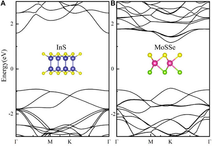
FIGURE 1. Band structures of (A) InS and (B) MoSSe monolayers.
For the MoSSe/InS vdWH, after considering the different stacking patterns between the layers, there are six typical stacking configurations, see Figure 2. Among them, I-III correspond to the cases when Se atoms are adjacent to InS monolayer, IV-VI correspond to the cases when S atoms are adjacent to InS monolayer. In order to compare the stability of the six configurations, their binding energies are calculated according to the formula:
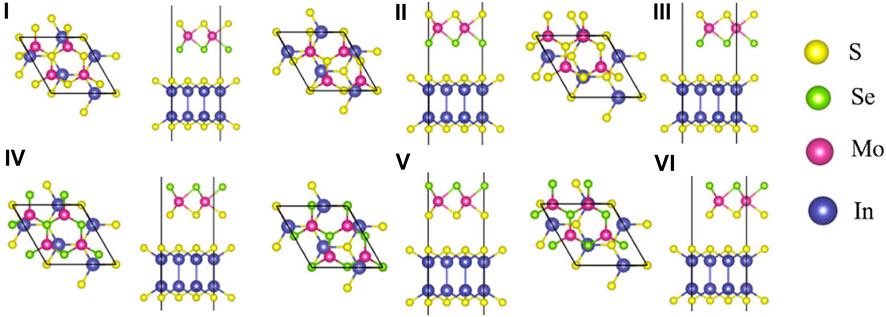
FIGURE 2. The top and side views of six stacking patterns of the MoSSe/InS vdWHs. The yellow, green, purple and blue balls represent the S, Se, Mo and In atoms, respectively.
In order to verify the thermodynamical stability, we perform ab initio molecular dynamics (AIMD) calculations for the MoSSe/InS vdWH at 300 K, as shown in Figure 3A. The simulations last for 3 ps with a time step of 0.5 fs. In the calculation of AIMD, the energy fluctuation of the vdWH is very small and the structure has no distortion, indicating that the vdWH has good thermal stability.
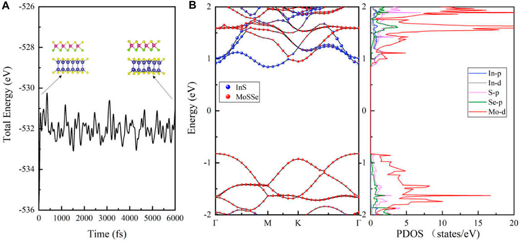
FIGURE 3. (A) The total energy and the crystal structures calculated from the AIMD of the MoSSe/InSe vdWH. (B) The projected band structures and the PDOS of the MoSSe/InS vdWH.
Figure 3B shows the projected band structure and the projected density of states (PDOS) of the MoSSe/InS vdWH calculated by HSE06 functional. In Figure 3B, it can be seen that the MoSSe/InS vdWH is an indirect band gap semiconductor with a band gap value of 1.67 eV, which is slightly smaller than those of MoSSe and InS monolayers and larger than the redox potential energy of water (1.23 eV). In addition, its CBM and VBM are located at M point and Γ point respectively, and it has type-Ⅱ band alignment because its CBM and VBM are contributed from InS and MoSSe monolayers respectively. The type-Ⅱ band alignment can effectively promote the spontaneous separation of electron-hole pairs, making it applicable to various photocatalytic and solar energy conversion devices (Massicotte et al., 2016; Lei et al., 2019). The PDOS also proves our suggestion. It can be seen that the CBM is mainly contributed from the In-p, In-d and S-p orbitals, and the VBM is mainly contributed from the Mo-d orbitals.
As shown in Figure 4A, the band decomposition charge densities of CBM and VBM are calculated. CBM and VBM are concentrated in the InS and MoSSe layers respectively, which means that the electrons are located in the InS layer and the holes are located in the MoSSe layer, respectively. In order to further understand the charge transfer mechanism between MoSSe and InS, we calculate the electrostatic potential and the charge density differences of the MoSSe/InS vdWH, as shown in Figure 4B. The red dotted line and the blue dotted line represent the vacuum level (Evac) and the Fermi level (Ef), respectively, and Φ is the work function which can be obtained by the difference between Evac and Ef, and its value is 5.51 eV. The charge density difference is in the lower left corner of Figure 4B, which is given by
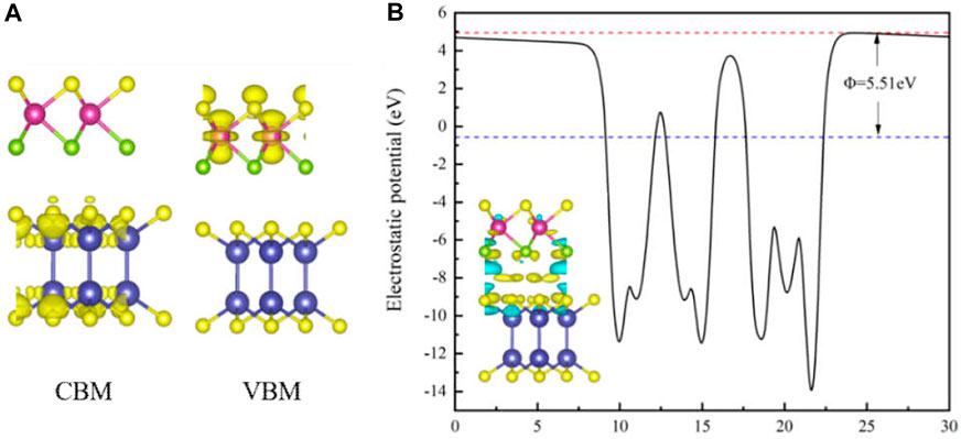
FIGURE 4. (A) The band decomposition charge densities of CBM and VBM for the MoSSe/InSe vdWH. (B) The electrostatic potential and the charge density difference of the MoSSe/InS vdWH.
2D materials can withstand greater strain than three-dimensional materials, so biaxial strain is a method that can effectively modulate the electronic structure and the optical properties of 2D materials (Guo et al., 2020; Zhu et al., 2021). In this paper, we study the effect of biaxial strain on the band gap, band edge position and the optical absorption of the MoSSe/InS vdWH. The biaxial strain can be defined as ε= (a−a0)/a0×100%, where a0 and a are the lattice constants of the strained-free and strained structures, correspondingly. In Figure 5A, the blue dashed line marks the redox potentials of H2O/O2 (−5.67 eV) and H+/H2 (−4.44 eV) of water. It can be seen that both the unstrained and strained band edges of the MoSSe/InS vdWH cross the oxidation potential of H2O/O2, so they are suitable for driving oxygen evolution reaction kinetics when pH = 0. In addition, when the applied pressure and tension increase, the energy levels of the CBM and the VBM move down and up, respectively. Figure 5B illustrates that the band gap of the MoSSe/InS vdWH decreases when the tensile strain increase, however, when the compressive strain increases, the band gap firstly reaches to a maximum and then decrease. This tunable band gap has potential applications in devices.
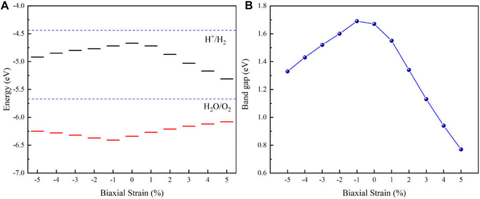
FIGURE 5. (A) Band edge positions and (B) band gap of the MoSSe/InS vdWH under various biaxial strains from −5 to 5%.
The optical absorption is calculated by the formula,
where ω is the light frequency,
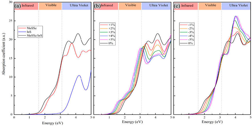
FIGURE 6. (A) The optical absorption spectra of MoSSe monolayer, InS monolayer and the MoSSe/InS vdWHs, (B,C) correspond to the cases with tension strain and compressive strain, respectively.
In summary, we have explored the electronic structure and the optical properties of the MoSSe/InS vdWH by first-principles calculations. Our results show that the MoSSe/InS vdWH has an indirect band gap with typical type-II band alignment that can effectively promote the spontaneous separation of electron-hole pairs. CBM and VBM are contributed from InS and MoSSe monolayers respectively, and electrons are transferred from the MoSSe layer into the InS layer in MoSSe/InS vdWH. Compared with monolayers, the carrier mobility and the optical absorption of the vdWH are enhanced. After the application of biaxial strain, the position of the band edge is adjusted, and the band gap of the vdWH can also be tuned. In the visible light region, the optical absorption intensity of the MoSSe/InS vdWH increases with the increasing of the tensile strain, and it decreases with the increasing of the compressive strain. Our work shows that the MoSSe/InS vdWH may have potential applications in optoelectronic devices.
The original contributions presented in the study are included in the article/Supplementary Material, further inquiries can be directed to the corresponding authors.
XY and YG did the calculations and wrote the paper, JW collected the references, GH prepared the figures, JR analyzed the data, XZ generated the research idea. All authors read and approved the final manuscript.
This work was supported by the National Natural Science Foundation of China (Grant Nos. 11674197 and 11974215), the Natural Science Foundation of Shandong Province (Grant No. ZR2021MA105), and the Qingchuang Science and Technology Plan of Shandong Province (No. 2019KJJ014).
The authors declare that the research was conducted in the absence of any commercial or financial relationships that could be construed as a potential conflict of interest.
All claims expressed in this article are solely those of the authors and do not necessarily represent those of their affiliated organizations, or those of the publisher, the editors and the reviewers. Any product that may be evaluated in this article, or claim that may be made by its manufacturer, is not guaranteed or endorsed by the publisher.
Blöchl, P. E. (1994). Projector Augmented-Wave Method. Phys. Rev. B 50, 17953–17979. doi:10.1103/physrevb.50.17953
Chen, D., Lei, X., Wang, Y., Zhong, S., Liu, G., Xu, B., et al. (2019). Tunable electronic structures in BP/MoSSe van der Waals heterostructures by external electric field and strain. Appl. Surf. Sci. 497, 143809. doi:10.1016/j.apsusc.2019.143809
Choi, W., Choudhary, N., Han, G. H., Park, J., Akinwande, D., and Lee, Y. H. (2017). Recent Development of Two-Dimensional Transition Metal Dichalcogenides and Their Applications. Mater. Today 20, 116–130. doi:10.1016/j.mattod.2016.10.002
Fleurence, A., Friedlein, R., Ozaki, T., Kawai, H., Wang, Y., and Yamada-Takamura, Y. (2012). Experimental Evidence for Epitaxial Silicene on Diboride Thin Films. Phys. Rev. Lett. 108, 245501. doi:10.1103/physrevlett.108.245501
Grimme, S., Antony, J., Ehrlich, S., and Krieg, H. (2010). A Consistent and Accurate Ab Initio Parametrization of Density Functional Dispersion Correction (DFT-D) for the 94 Elements H-Pu. J. Chem. Phys. 132, 154104. doi:10.1063/1.3382344
Grimme, S., Ehrlich, S., and Goerigk, L. (2011). Effect of the Damping Function in Dispersion Corrected Density Functional Theory. J. Comput. Chem. 32, 1456–1465. doi:10.1002/jcc.21759
Guo, H., Zhang, Z., Huang, B., Wang, X., Niu, H., Guo, Y., et al. (2020). Theoretical study on the photocatalytic properties of 2D InX(X = S, Se)/transition metal disulfide (MoS2 and WS2) van der Waals heterostructures. Nanoscale 12, 20025–20032. doi:10.1039/d0nr04725b
Guo, J. T., Zhao, X. W., Hu, G. C., Ren, J. F., and Yuan, X. B. (2021). Observation and Manipulation of valley Polarization in Two-Dimensional H-Tl2O/CrI3 Heterostructure. Appl. Surf. Sci. 558, 149604. doi:10.1016/j.apsusc.2021.149604
Guo, Y. H., Wang, J. L., Hu, G. C., Yuan, X. B., and Ren, J. F. (2021). Strain-tunable electronic and optical properties of novel MoSSe/InSe van der Waals heterostructures. Phys. Lett. A 404, 127395. doi:10.1016/j.physleta.2021.127395
Heyd, J., Scuseria, G. E., and Ernzerhof, M. (2003). Hybrid Functionals Based on a Screened Coulomb Potential. J. Chem. Phys. 118, 8207–8215. doi:10.1063/1.1564060
Hollingsworth, J. A., Poojary, D. M., Clearfield, A., and Buhro, W. E. (2000). Catalyzed Growth of a Metastable InS Crystal Structure as Colloidal Crystals. J. Am. Chem. Soc. 122, 3562–3563. doi:10.1021/ja000106u
Huang, A., Shi, W., and Wang, Z. (2019). Optical Properties and Photocatalytic Applications of Two-Dimensional Janus Group-III Monochalcogenides. J. Phys. Chem. C 123, 11388–11396. doi:10.1021/acs.jpcc.8b12450
Hung, N. T., Nugraha, A. R. T., and Saito, R. (2017). Two-dimensional InSe as a Potential Thermoelectric Material. Appl. Phys. Lett. 111, 092107. doi:10.1063/1.5001184
Kresse, G., and Furthmüller, J. (1996). Efficient Iterative Schemes Forab Initiototal-Energy Calculations Using a Plane-Wave Basis Set. Phys. Rev. B 54, 11169–11186. doi:10.1103/physrevb.54.11169
Kresse, G., and Joubert, D. (1999). From Ultrasoft Pseudopotentials to the Projector Augmented-Wave Method. Phys. Rev. B 59, 1758–1775. doi:10.1103/physrevb.59.1758
Lei, C., Ma, Y., Xu, X., Zhang, T., Huang, B., and Dai, Y. (2019). Broken-Gap Type-III Band Alignment in WTe2/HfS2 van der Waals Heterostructure. J. Phys. Chem. C 123, 23089–23095. doi:10.1021/acs.jpcc.9b07862
Liu, Y.-L., Shi, Y., and Yang, C.-L. (2021). Two-dimensional MoSSe/g-GeC van der waals heterostructure as promising multifunctional system for solar energy conversion. Appl. Surf. Sci. 545, 148952. doi:10.1016/j.apsusc.2021.148952
Lu, A.-Y., Zhu, H., Xiao, J., Chuu, C.-P., Han, Y., Chiu, M.-H., et al. (2017). Janus Monolayers of Transition Metal Dichalcogenides. Nat. Nanotech 12, 744–749. doi:10.1038/nnano.2017.100
Massicotte, M., Schmidt, P., Vialla, F., Schädler, K. G., Reserbat-Plantey, A., Watanabe, K., et al. (2016). Picosecond photoresponse in van der Waals heterostructures. Nat. Nanotech 11, 42–46. doi:10.1038/nnano.2015.227
Miao, M.-S., Botana, J., Zurek, E., Hu, T., Liu, J., and Yang, W. (2016). Electron Counting and a Large Family of Two-Dimensional Semiconductors. Chem. Mater. 28, 1994–1999. doi:10.1021/acs.chemmater.5b03557
Novoselov, K. S., Geim, A. K., Morozov, S. V., Jiang, D., Zhang, Y., Dubonos, S. V., et al. (2004). Electric Field Effect in Atomically Thin Carbon Films. Science 306, 666–669. doi:10.1126/science.1102896
Obeid, M. M., Bafekry, A., Ur Rehman, S., and Nguyen, C. V. (2020). A type-II GaSe/HfS2 van der Waals heterostructure as promising photocatalyst with high carrier mobility. Appl. Surf. Sci. 534, 147607. doi:10.1016/j.apsusc.2020.147607
Özçelik, V. O., Azadani, J. G., Yang, C., Koester, S. J., and Low, T. (2016). Band Alignment of Two-Dimensional Semiconductors for Designing Heterostructures With Momentum Space Matching. Phys. Rev. B 94, 035125. doi:10.1103/PhysRevB.94.035125
Perdew, J. P., Burke, K., and Ernzerhof, M. (1996). Generalized Gradient Approximation Made Simple. Phys. Rev. Lett. 77, 3865–3868. doi:10.1103/physrevlett.77.3865
Qiu, B., Zhao, X. W., Hu, G. C., Yue, W. W., Yuan, X. B., and Ren, J. F. (2020). Tuning Optical Properties of Graphene/WSe2 Heterostructure by Introducing Vacancy: First Principles Calculations. Physica E: Low-dimensional Syst. Nanostructures 116, 113729. doi:10.1016/j.physe.2019.113729
Ren, K., Zheng, R., Lou, J., Yu, J., Sun, Q., and Li, J. (2021). Ab Initio Calculations for the Electronic, Interfacial and Optical Properties of Two-Dimensional AlN/Zr2CO2 Heterostructure. Front. Chem. 9, 796695. doi:10.3389/fchem.2021.796695
Ren, K., Zheng, R., Xu, P., Cheng, D., Huo, W., Yu, J., et al. (2021). Electronic and Optical Properties of Atomic-Scale Heterostructure Based on MXene and MN (M = Al, Ga): A DFT Investigation. Nanomaterials 11, 2236. doi:10.3390/nano11092236
Ren, K., Zheng, R., Yu, J., Sun, Q., and Li, J. (2021). Band Bending Mechanism in CdO/Arsenene Heterostructure: A Potential Direct Z-Scheme Photocatalyst. Front. Chem. 9, 788813. doi:10.3389/fchem.2021.788813
Shen, Z., Ren, K., Zheng, R., Huang, Z., Cui, Z., Zheng, Z., et al. (2022). The Thermal and Electronic Properties of the Lateral Janus MoSSe/WSSe Heterostructure. Front. Mater. 9, 838648. doi:10.3389/fmats.2022.838648
Sun, R. J., Lu, J. J., Zhao, X. W., Hu, G. C., Yuan, X. B., and Ren, J. F. (2022). Robust Valley Polarization Induced by Super-Exchange Effects in HfNX (X= Cl, Br, I)/FeCl2 Two-Dimensional Ferrovalley Heterostructures. Appl. Phys. Lett. 120, 063103. doi:10.1063/5.0080466
Wang, V., Xu, N., Liu, J. C., Tang, G., and Geng, W.-T. (2021). VASPKIT: A User-Friendly Interface Facilitating High-Throughput Computing and Analysis Using VASP Code. Comput. Phys. Commun. 267, 108033. doi:10.1016/j.cpc.2021.108033
Wu, W., Ao, Z., Wang, T., Li, C., and Li, S. (2014). Electric Field Induced Hydrogenation of Silicene. Phys. Chem. Chem. Phys. 16, 16588–16594. doi:10.1039/c4cp01416b
Xu, K., Yin, L., Huang, Y., Shifa, T. A., Chu, J., Wang, F., et al. (2016). Synthesis, Properties and Applications of 2D Layered MIIIXVI(M = Ga, in; X = S, Se, Te) Materials. Nanoscale 8, 16802–16818. doi:10.1039/c6nr05976g
Yin, W.-J., Wen, B., Nie, G.-Z., Wei, X.-L., and Liu, L.-M. (2018). Tunable Dipole and Carrier Mobility for a Few Layer Janus MoSSe Structure. J. Mater. Chem. C 6, 1693–1700. doi:10.1039/c7tc05225a
Zhang, J., Jia, S., Kholmanov, I., Dong, L., Er, D., Chen, W., et al. (2017). Janus Monolayer Transition-Metal Dichalcogenides. ACS Nano 11, 8192–8198. doi:10.1021/acsnano.7b03186
Zhang, W. X., Yin, Y., and He, C. (2021). P Doping Promotes the Spontaneous Visible-Light-Driven Photocatalytic Water Splitting in Isomorphic Type II GaSe/InS Heterostructure. J. Phys. Chem. Lett. 12, 7892–7900. doi:10.1021/acs.jpclett.1c02040
Zhao, X. W., Liu, F. J., Ren, J. F., and Qu, F. Y. (2021). Valleytronic and Magneto-Optical Properties of Janus and Conventional TiBrI/CrI3 and Ti X2/CrI3 (X= Br, I) Heterostructures. Phys. Rev. B. 104, 085119. doi:10.1103/physrevb.104.085119
Zhou, J., Li, D., Zhao, W., Jing, B., Ao, Z., and An, T. (2021). First-Principles Evaluation of Volatile Organic Compounds Degradation in Z-Scheme Photocatalytic Systems: MXene and Graphitic-CN Heterostructures. ACS Appl. Mater. Inter. 13, 23843–23852. doi:10.1021/acsami.1c05617
Keywords: van der waals heterostructure, first principles calculations, optical absorption, biaxial strain, band edge position
Citation: Yuan XB, Guo YH, Wang JL, Hu GC, Ren JF and Zhao XW (2022) Type-II Band Alignment and Tunable Optical Absorption in MoSSe/InS van der Waals Heterostructure. Front. Chem. 10:861838. doi: 10.3389/fchem.2022.861838
Received: 25 January 2022; Accepted: 07 February 2022;
Published: 22 February 2022.
Edited by:
Guangzhao Wang, Yangtze Normal University, ChinaCopyright © 2022 Yuan, Guo, Wang, Hu, Ren and Zhao. This is an open-access article distributed under the terms of the Creative Commons Attribution License (CC BY). The use, distribution or reproduction in other forums is permitted, provided the original author(s) and the copyright owner(s) are credited and that the original publication in this journal is cited, in accordance with accepted academic practice. No use, distribution or reproduction is permitted which does not comply with these terms.
*Correspondence: J. F. Ren, cmVuamZAc2RudS5lZHUuY24=; X. W. Zhao, eHd6aGFvQHNkbnUuZWR1LmNu
Disclaimer: All claims expressed in this article are solely those of the authors and do not necessarily represent those of their affiliated organizations, or those of the publisher, the editors and the reviewers. Any product that may be evaluated in this article or claim that may be made by its manufacturer is not guaranteed or endorsed by the publisher.
Research integrity at Frontiers
Learn more about the work of our research integrity team to safeguard the quality of each article we publish.