 Laurynas Staišiūnas
 Putinas Kalinauskas
 Eimutis Juzeliūnas*
 Asta Grigucevičienė
 Konstantinas Leinartas
 Gediminas NiauraSandra StanionytėAlgirdas Selskis
- Centre for Physical Sciences and Technology, Vilnius, Lithuania
Hafnium oxide (HfO2) films on silicon have the potential for application in photovoltaic devices. However, very little is known about the photoelectrochemical and protective properties of HfO2 films on Si. In this study, ultrathin films of HfO2 in the range of 15–70 nm were deposited on p-Si and Au substrates by atomic layer deposition (ALD). Grazing incidence X-ray diffraction (GI-XRD) identified the amorphous structure of the layers. Quartz crystal nanogravimetry (QCN) with Si and Au substrates indicated dynamics of electrolyte intake into the oxide film. No indications of oxide dissolution have been observed in acid (pH 3) and alkaline (pH 12) electrolytes. Mott–Schottky plots showed that the dark Si surface adjacent to the SiHfO2 interface is positively charged in an acid electrolyte and negatively charged in an alkaline electrolyte. The number of photoelectrons was determined to be much greater than the doping level of silicon. The cathodic photoactivity of the p-Si electrode protected by HfO2 films was studied with respect to the reaction of hydrogen reduction in acid and alkaline solutions. In acid solution, the film enhanced the reduction process when compared to that on the coating free electrode. The acceleration effect was explained in terms of prevention of silicon oxide formation, whose passivating capability is higher than that of hafnia films. In an alkaline electrolyte, an inhibition effect of the film was determined. Hafnia films protected Si from corrosion in this medium; however, at the same time, the film reduced electrode activity.
Introduction
Thin films of metal oxides are promising materials for the protection of semiconductors from aggressive environments and improving of their stability. Electrochemical instability of silicon (Si) in electrolytes is an issue, which has impeded the development of sunlight-driven photovoltaic (PV) systems for water splitting (Hu et al., 2015). Several oxides have been studied for protection of p-Si photocathodes, for example, TiO2 (Seger et al., 2013), ZnO (Sun et al., 2012), SiOx (Esposito et al., 2013; Choi et al., 2014), Al2O3 (Choi et al., 2014), and SrTiO3 (Ji et al., 2015). Hafnium oxide (hafnia, HfO2) is a potential candidate for Si protection due to its high chemical inertness, optical transparency, wide band gap, and high dielectric constant.
Passivation effects by hafnium oxide for efficiency enhancement in organic and inorganic solar cells have recently been reported (Polydorou et al., 2018; Cui et al., 2017b; Singh et al., 2016; Oudot et al., 2018). A p-type Si with a 15-nm hafnia film showed an effective surface recombination velocity of 9.9 cm s−1 and an interface state density of 3.6 × 1010 cm−2 eV−1 (Cui et al., 2017b). Efficiency of Si photocathodes with a HfO2 interlayer between a p+/n/n+ structure and a Ni3N/Ni cocatalyst was studied (Zhanget al. 2021). It was shown that a 1-nm HfO2 interlayer enhanced the electrode efficiency by 9%. A p-Si substrate was protected by a HfOx/SiOx bilayer used in the hybridization of the photoelectrochemical (PEC) device with a thermoelectric device (Jung et al., 2019). Protection of Si surface nanostructures by HfO2 was also studied (Xing et al., 2017). The authors concluded that the HfO2 layer on nanoporous Si was less stable than the TiO2 layer.
Passivation in photovoltaics (PV) and electrochemistry refers to different, albeit related, phenomena. Electronic passivation in PV addresses reduction of interface state density (Dif) (unsaturated bonds) on the semiconductor surface, for example, by chemical reduction applying passivating dielectrics (Cui et al., 2017a; Singh et al., 2016; Oudot et al., 2018). Another important type is the field effect passivation, which relates to electrostatic shielding of the charge carriers from the interface by an internal electric field, for example, films having a negative (Al2O3, SiO2+HfO2) or positive (SiNx) charge (Singh et al., 2016; Oudot et al., 2018).
Electrochemical passivation refers primarily to the inhibition of the charge transfer from semiconductor to electrolyte, or vice versa. To this end, the semiconductor is coated with a layer that protects the substrate from aggressive environments and prevents electron transfer to the electrolyte (Hu et al., 2015; Seger et al., 2013; Sun et al., 2012; Esposito et al., 2013; Choi et al., 2014; Ji et al., 2015). Another kind of passivation is the spontaneous formation of protective films from corrosion products (Hu et al., 2015). It is desirable for a photo-electrode that the passive layer can reduce recombination velocity, protect the Si–electrolyte junction from corrosion, and not inhibit substantially the electron transfer to electrolyte, that is, the layer does not reduce efficiency of (photo) electrochemical process. However, in most cases, oxide films mitigate Si corrosion at the expense of surface activity: the electrode becomes electrochemically inactive in certain potential regions. The dilemma is typically solved in favor of passivity because dissolution leads to continual destruction of the semiconductor and failure propagation throughout active regions (Hu et al., 2015).
Hafnium oxide is a highly resistive material; its dielectric constant is several times higher than conventional silica gate dielectrics (Chen et al., 2010). The Pourbaix diagram shows the formation of a stable passive oxide on hafnium over the entire potential pH range (Pourbaix, 1974). Due to these features, thin layers of the oxide were applied for anticorrosion protection of stainless steel (304 SS) (Li et al., 2019) or magnesium alloys (Staišiūnas et al., 2020).
Hafnia films were obtained by various techniques such as RF and DC magnetron sputtering (Verelli and Tsoukalas, 2011; Dave et al., 2018), electrochemical anodizing (Fohlerova and Mozalev, 2019), electron beam evaporation (Ramzan et al., 2015), ultrasonic spray pyrolysis (Mendoza et al., 2010), UV-stimulated plasma anodizing (Kushitashvili et al., 2017), pulsed laser deposition (Plociennik et al., 2014), and electrochemical formation in organic electrolytes (Wang et al., 2017). Atomic layer deposition (ALD) is most widely used to form thin hafnia films and microstructures (Polydorou et al., 2018; Cui et al., 2017a; Singh et al., 2016; Oudot et al., 2018; Chen et al., 2010; Li et al., 2019; Zhang et al., 2017b; Ortiz-Dosal et al., 2017; Gaskins et al., 2017; Berdova and Liu, 2016). Thermal, mechanical, electrical, optical, and structural properties of ALD-formed HfO2 have recently been investigated and reviewed (Gaskins et al., 2017; Berdova and Liu, 2016; Jogiaas et al., 2015).
Little is known about photoelectrochemical (PEC) and protective properties of HfO2 films on Si in electrolytes. PEC studies are important for PV in many aspects. They provide information that correlates with that of the solid-state cells, so that there is no prior need to design a solar cell that characterizes Si surface photo-responsiveness (Cho et al., 2012; Ye et al., 2011). The PEC characterization can provide information about Si surface stability and its charging as well as the electron transfer from Si to electroactive species in the electrolyte—the process that is at the heart of PV devices for solar-driven hydrogen production. Here, we address the aforementioned questions performing the PEC measurements at open circuit and in wide range of cathodic polarizations in acid and alkaline mediums.
At the same time, the presence of electrolyte presupposes some complexity of the subject. In particular, the adsorption of hydrogen or hydroxide ions can influence the interfacial properties of the Si–oxide system. Distortion of oxide surfaces by penetration of electrolyte is a phenomenon of general nature (Perram et al., 1974). Water incorporation into the oxide layer could reduce its density, refraction index, or acoustic velocity (Davis and Tomozawa, 1995). Proton and water penetration into oxide is of importance to understand the instability of dielectrics during the operation of ion-sensitive field effect transistors (ISFETs). The presence of water or hydrogen-related species (–H, –OH) in ISFETs could enhance interface state generation and charge trapping (Topkar and Lal, 1995; Hazarika and Sharma, 2014). We studied here the electrolyte absorption by the hafnia film using mass change as a criterion. To that end, the quartz crystal nanobalance (QCN) was used, which provides information in situ and in real time with nanogram resolution.
Experimental
P-type <100> silicon wafers from Si-Mat GmbH, Germany were used. Wafer diameter was 5 cm, the geometric area—22.8 cm2, the thickness – 275 ± 25 μm, and the resistivity was 10–20 Ω cm−1. The wafer surface was polished. The p-Si with thermal 10-nm SiO2 film was used as received from Si-Mat GmbH. XRD confirmed the amorphous structure of the silica layer.
HfO2 films were grown by ALD on the specimens 1 cm × 1 cm cut from the Si wafers. The ALD reactor Fiji F200 from Cambridge Nanotech has been used. The native oxide has been removed from the silicon surface using H2O2 + H2SO4 (1:1) and HF (1 HF: 40 H2O) solution. Tetrakis(dimethylamino)-Hf (TDMAH, [(CH3)2N]4Hf) from Strem Chemicals, Inc. and distilled water were used as hafnium and oxygen precursors. TDMAH and H2O were evaporated at 85 and 20°C, respectively. Argon was used as a carrier gas at a constant flow rate of 260 sccm. The HfO2 deposition temperature of 200°C and base pressure of ∼0.33 mbar were set in the deposition chamber. The deposition cycle consisted of a 0.06 s pulse of water, a 5 s purge, a 0.2 s pulse of TDMAH, and a 5 s purge. ALD is based on chemical self-limiting surface reactions, and the thickness of the coating is proportional to the number of cycles in the deposition sequence. Our estimations showed a linear dependence of the thickness vs. deposition cycles with a slope ∼0.13 nm/cycle within the 9–80 nm range. Basic principles of ALD were well reviewed (Miikkulainen et al., 2013; Schwartzberg and Olynick, 2015).
The thickness of the ALD hafnia layers was evaluated by the spectroscopic ellipsometry technique using a dual rotating compensator ellipsometer RC2 from J.A. Woollam, Co., Inc. The morphology and composition of the deposits were examined by SEM Helios NanoLab 650 from FEI equipped with an energy-dispersive X-ray spectrometer (EDX) from INCA Energy from Oxford Instruments.
Structural properties of the films were studied by the grazing incidence X-ray diffraction (GI-XRD) using a SmartLab diffractometer from Rigaku with an X-ray tube equipped with 9 kW Cu rotating anode. Grazing incidence geometry was used with the angle of the Cu Kα beam set to 0.5°, which enables investigation of thin films and reduces the influence of the substrate. A continuous scan mode was used in the 2Θ range from 15° ≤ 2θ ≤ 60° with a step of 0.02° and speed of 2.5°min−1.
The PEC measurements were carried out in an acid NaClO4 solution adjusted by hydrochloric acid to pH 3 and in NaOH diluted to pH 12. The measurements were conducted in a glass cell equipped with a quartz window using Luxeon 3W LED irradiation of λ = 505 nm wavelength and the energy density of 50 mW cm−2. Film transparency (Tr) has been evaluated using a reflectance calculator, which is based on the complex matrix form of the Fresnel equations (www.filmetrics.com/reflectance-calculator). Calculations at λ = 505 nm showed that HfO2 films of 10 nm in thickness are almost completely transparent (Tr = 0.972), while 60-nm films transmit about 67% of the light (Tr = 0.667).
The measurements have been taken using PARSTAT 2273 equipment from Princeton Applied Research. The Hg/HgSO4 electrode in 0.5 M H2SO4 from International Chemistry Co., LTD was used as a reference electrode. The potential of this electrode was E0 = 0.612 V vs. the normal hydrogen electrode (NHE) at 25°C, and the measured potentials all through the paper are given with respect to NHE. The counter electrode was a 4-cm2 Pt plate. The working electrode was mounted in an electrochemical glass cell so that the area of the electrode exposed to the electrolyte was 0.5 cm2 (Figure 1). The entire voltage applied to the cell comprised of several contributions: the drops in the electrolyte, within the hafnia film, the Si wafer, and the native silicon oxide in contact with the metallic conductor on the cell backside. The polarization curves were measured in a potentiodynamic mode at a potential scan rate of 0.5 mV s−1. Mott–Schottky plots were obtained at a frequency of 1 kHz using the PARSTAT 2273 equipment.
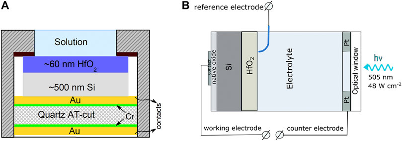
FIGURE 1. (A) Principal configuration of the QCN sensor, which is composed of Cr/Au/Si/HfO2 layers on quartz. Silicon layer was formed by RF magnetron sputtering, and HfO2 layer was formed by ALD; (B) experimental setup of the PEC measurements.
The QCN measurements were performed at ambient temperature (20 ± 2°C) using the P/G/FRA system Autolab 302 from Metrohm AG, equipped with the Quartz Crystal Microbalance QCM 922 unit from Princeton Applied Research. AT-cut quartz resonators with Au electrodes produced by Intellemetrics Global Ltd were used to prepare the quartz crystal nanogravimetry sensors (Figure 1A). Si layer has been sputtered on the Au sublayer using a Univex 350 from Leybold Vacuum GmbH. As a sputtering target, the p-Si wafer was used. Before deposition, the sputtering chamber was evacuated to ∼2 × 10⁻⁴ Pa pressure and filled with Ar (99.999%). The working pressure of the chamber was maintained at 0.19 Pa, and the substrate temperature was set at 50°C. The sputtering time was 15 min, and the sputtering power was 25 W, which yielded a coating of ∼0.2 μm thickness. The HfO2 layer on the Si surface was deposited by ALD, as described before. The fundamental frequency of the sensor was f0 = 6 MHz, and the sensitivity factor was K = 12.4 ng Hz−1 cm−−2. The principal configuration of the mass sensor and the electrochemical cell is shown in Figure 1.
The morphology and composition of the deposits were examined by a SEM Helios NanoLab 650 from FEI equipped with an energy-dispersive X-ray spectrometer (EDX) from INCAEnergy from Oxford Instruments.
Raman spectra were recorded using a confocal spectrometer in Via (Renishaw, United Kingdom) equipped with a thermoelectrically cooled CCD detector (−70°C) and a microscope. Raman spectra were excited with 532-nm radiation from the CW diode-pumped solid-state (DPSS) laser (Renishaw, United Kingdom). The laser power at the sample was restricted to 0.6 mW. The 50x/0.75 NA objective lens and 1800 lines/mm grating were used to record the Raman spectra. The overall integration time was 800 s.
Results and Discussion
Structural Study
The structural properties of the ALD HfO2 films were studied by GI-XRD (Figure 2). The grazing incidence geometry of this method enables investigation of the crystallographic structure of thin films and reduces the influence of the silicon substrate. The GI-XRD provided reliable structural data of HfO2 and ZrO2 thin films from ∼9 to ∼30 nm in thickness (Park et al., 2017; Sharma et al., 2017).
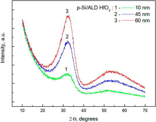
FIGURE 2. GI-XRD patterns obtained for p-Si with ALD deposited HfO2 layers of different thickness: 10, 45, and 60 nm.
The XRD data do not indicate crystallinity features of the films—a broad peak at 2Θ ∼ 33° indicates an amorphous structure. A similar peak was observed for amorphous HfO2 nanoparticles with diameter ∼4 nm prepared by the ammonia catalyzed hydrolysis and condensation of hafnium (IV) tert-butoxide (Chaubey et al., 2012). The authors showed that the amorphous structure did not change during annealing of the samples up to 400°C; indications of monoclinic HfO2 phase appeared at 500 °C or higher. Our study showed appearance of HfO2 crystallinity with a monoclinic structure when coating thickness has been increased to 80 nm (Staišiūnas et al., 2020).
Crystallization phenomena of HfO2 nanofilms have attracted considerable attention (Cui et al., 2017b; Singh et al., 2016; Kim at al., 2003; Fan et al., 2012; Zhang et al., 2019). The crystallinity of the films is important in terms of Si surface passivation. The films on silicon up to 35 nm in thickness were found predominantly amorphous with minor localized nucleation of crystals (Cui et al., 2017b; Singh et al., 2016). The amorphous structure yielded highly effective electronic passivation, whereas the film crystallization achieved by annealing at higher temperatures led to degradation of the effective surface recombination velocity. Thickness-dependent crystallization was also studied for the films obtained by ion-assisted RF deposition (Zhang et al., 2017). The authors observed the formation of grains when the coating thickness was greater than 12 nm. The grain size and density increased with the coating thickness. This phenomenon was explained in terms of the Gibbs energy change of the atom clusters. The crystallization depends on the ratio between the cluster surface area and its volume. Thinner coatings have a smaller cluster size and a higher surface-to-volume ratio; this results in a positive change in Gibbs energy and suppression of the amorphous-to-crystalline transformation. In the present study, such suppression is likely due to the deposition of extremely thin single layers using a layer-by-layer ALD approach (∼0.13 nm/cycle). The produced films, therefore, did not show appreciable crystallinity in the studied thickness range.
Nanogravimetry and Raman Spectroscopy
Nanogravimetry provides sensitively the data on the instability of Si–HfO2 electrode, which results in a change in electrode mass (Figure 3). The measurement shows in situ and real-time mass change with nanogram resolution immediately after the sample comes into contact with the electrolyte.
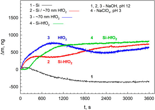
FIGURE 3. Mass change determined by the QCN of the samples with 70-nm HfO2 layer on Si (2, 4) and Au (3) substrates when exposed in NaOH (pH 12) (1–3) and 1 M NaClO4 adjusted to pH 3 (4). Curve 1 shows the mass change of hafnia-free silicon pretreated in an HF solution.
The nanogravimetric data obtained for the Au–HfO2 electrode indicate an increase in electrode mass during the exposure. With time, the mass becomes more or less constant for all electrodes. Note that the mass change of the Au–HfO2 electrode does not differ greatly from that of the Si–HfO2 electrode. Due to the chemical inertness of the Au substrate, the mass gain is attributable to the events within the oxide film, most likely, the electrolyte absorption by the film. The mass of the film increased on average by up to Δm ∼ 700 ng cm−2 during 1 hour of exposure. An increase in the mass of the film on the Si substrate was of similar value. There were no indications observed of oxide dissolution, which would be detected as a decrease in electrode mass. This implies effective electrode protection by the hafnia film both in acidic and alkaline media. As commonly known, silicon is stable in water and acidic solutions due to the formation of a stable protective oxide. This oxide, however, is unstable in alkaline solutions. Chemical and electrochemical corrosion could contribute to the mass effect in alkaline solutions (Hu et al., 2015). The mass decrease in the electrode unprotected with a hafnia coating indicates the corrosion process. With time, the dissolution ceases due to surface passivation by corrosion products.
It is also important that the mass curve for the Si–HfO2 electrode in acid solution does not differ greatly from that in alkaline solution (Figure 3). Thus, the amount of the absorbed electrolyte does not depend on solution acidity, and the mass effect is similar as the densities of both electrolytes do not differ considerably. The mass of the HfO2 layer 70 nm in thickness is calculated to be m = 63 μg cm−2 assuming its density, dHfO2 = 9.68 g cm−3. The electrolyte intake is Δm ∼ 0.7 μg cm−2; this corresponds to ∼4.4% of the initial oxide mass. The volume of accommodated solution will make up approximately ∼50% of the initial oxide volume.
The QCN data show that the electrolyte penetrates the thin oxide film and transforms it to a hybrid electrode Si–HfO2–electrolyte. The electrolyte plays an essential role in interfacial charging.
The question also arises about perchlorate penetration into the oxide layer, first of all, due to the presence of non-uniformities and defect sites in the surface layer. Raman spectroscopy implied that perchlorate ions do not enter appreciably the oxide layer during illumination; they are retained at the oxide/electrolyte boundary. This method is applied for effective detection and discrimination of oxyanions. Perchlorate possesses a relatively high Raman cross section (12.7 × 10⁻³⁰ cm2 sr−1 molecule−1) (McCreery, 2002) and can be determined by normal Raman as well as surface-enhanced Raman spectroscopy (SERS) approaches (Hao and Meng, 2017). The detection limits range from micromolar to nanomolar levels (10–6–10–9 M; 0.1 mg L−1–0.1 μg L−1). To that end, various SERS substrates mainly based on gold and silver are used: functionalized gold–silica (Au–SiO2) (Wang et al., 2006), 2-dimethylaminoethanethiol (DMAE)-modified gold nanoparticles (Gu et al., 2009), silver, gold, silver–gold, and selective sorbents (Wang and Gu, 2005; Nuntawong et al., 2013; Gu et al., 2004; Byram et al., 2018; Jubb et al., 2017). Also, the discrimination of perchlorate from salt mixtures has been demonstrated by Raman spectroscopy (Zapata and Garcia-Ruiz, 2018).
Figure 4 compares the Raman spectrum of a radiation-treated Si–HfO2 sample with the spectrum of a Si reference. P-type Si with a 60-nm HfO2 layer has been pre-exposed in 1 M perchlorate electrolyte for 5 min, illuminated for 5 min by λ = 505 nm light, and withdrawn from the electrolyte. The broad and intense band between 920 and 1,050 cm−1 belongs to the second-order Raman spectrum of the silicon substrate (Gillet et al., 2017). Observed spectral features are very similar with silicon substrate Raman spectrum. The Raman spectrum of 0.1 M NaClO4 aqueous solution (Figure 4B) exhibits a well-defined band at 934.6 cm−1 associated with the symmetric stretching vibration of the ClO4− ion (Zdaniauskienė et al., 2018; Niaura and Malinauskas, 1998). To enhance small spectral changes, we have constructed a difference spectrum. However, this spectrum does not indicate the presence of any additional bands compared with the silicon substrate. Thus, the Raman spectroscopy study does not provide any evidence confirming the presence of ClO4− ions in the studied Si–HfO2 structure. Thus, one could conclude that the mass gain observed by the QCN (Figure 3) was due to the incorporation of water along with protons and hydroxyl. Protons could increase the state density at the Si/oxide interface, and such modification could form some areas of an interconnected network of defective regions (Topkar and Lal, 1995). Penetration of water could create increased mobility paths for the protons (Topkar and Lal, 1995).
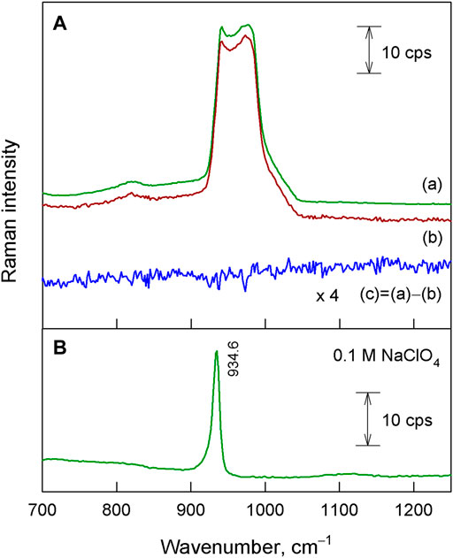
FIGURE 4. (A) Raman spectra of Si–HfO2 treated with radiation in NaClO4 solution (a) and Si reference sample (b). Difference spectrum (c) with a magnified intensity (×4) is also shown. Spectra are shifted vertically for clarity. (B) Raman spectrum of 0.1 M NaClO4 aqueous solution. Excitation wavelength is 532 nm.
Photoeffects
The PEC measurements have been performed using λ = 505 nm illumination, which is around the middle of the visible spectrum (∼380 to ∼750 nm). The applied photon energy (2.45 eV) is greater than the bandgap energy of Si (Eg,Si = 1.1 eV); it was sufficient to excite the Si photoelectrons to the conduction band. Note that the bandgap of ALD HfO2 films under dry conditions is much higher (Eg,HfO2 = 5.9 ± 0.5 eV) (Cheynet et al., 2007). The oxide can retain its insulating properties in electrolyte as well, particularly, at early stages of exposure.
Figure 5 shows a measurement of the electrode capacitance (C) depending on the electrode negative polarization (-ΔE). The data are displayed as C−2 vs. E plots that are in accordance with the Mott–Schottky relation:
where CSC stands for space charge capacitance, ND/A means the number of donors or acceptors in the space charge layer, k is the Bolzmann’s constant, ε is the dielectric constant of the semiconductor, ε0 is the permittivity of free space, T is the absolute temperature, e is the charge of a hole or electron, and Efb is the flatband potential. Efb means the potential, at which the energy band bends to zero. This parameter can be determined when extrapolating the E–C−2 curve to C−2 = 0. The curve slope reflects the doping level of the dark electrode or the density of the photogenerated charges in the space charge region.
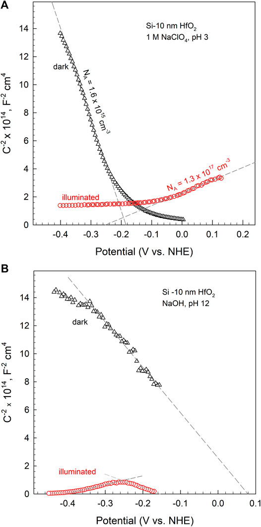
FIGURE 5. Mott–Schottky plots for p-Si with 10-nm HfO2 layer in the dark and under illumination (λ = 505 nm, N = 50 mW cm−2) in (A) 1M NaClO4 at pH 3 and (B) NaOH at pH 12. The electrode potential has been stepped from the open circuit in negative direction.
The electrodes in the studied potential range (Figure 5) were nearly ideally polarizable; no appreciable Faradaic process was observed under dark and illuminated conditions in this region, as Figures 6, 7 demonstrate. The capacitance values of the dark electrode were on the order of nanofarads (nF cm−2). Such low values indicate that the capacitances are attributable to the solid phase (e.g., space charge region), rather than the solid–solution interface. A double layer, which is formed by water and electrolyte ions (Helmholtz layer), typically has a capacitance on the order of microfarads (μF cm−2) (Bard and Faulkner, 2001; Zhang, 2004). As commonly known, C is in inverse proportion to the distance between positively and negatively charged zones. The space charge region can extend up to 2000 Å, while the Helmholtz layer is only several angstroms wide (Bard and Faulkner, 2001; Zhang, 2004). The lowest C value will predict the total capacitance (in analogy with the equivalent capacitance (Ceg) with actual capacitances (C1, C2) connected in series: 1/Ceq = 1/C1 + 1/C2).
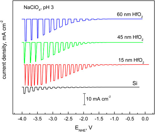
FIGURE 6. Cathodic photocurrents of hydrogen reduction over wide region of cathodic voltages obtained for p-Si–H electrode prepared by treatment in HF solution (marked as Si) and that coated with HfO2 layer with different thickness. Electrolyte: 1 M NaClO4 (pH 3). The illumination of 505-nm wavelengths and intensity of 50 mW cm−2 have been chopped at certain intervals. The potential sweep rate was 5 mV s−1.
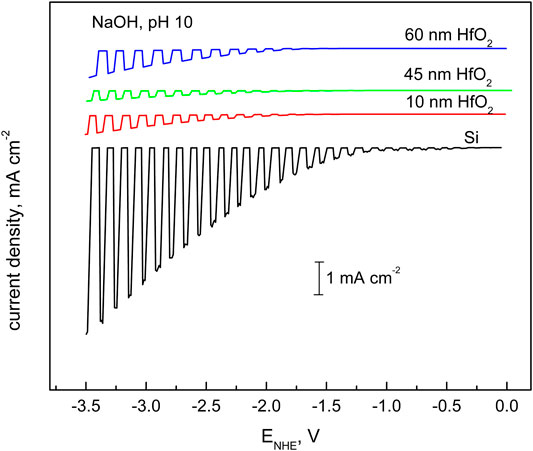
FIGURE 7. Cathodic photocurrents of hydrogen reduction over wide region of cathodic voltages obtained for p-Si–H electrode prepared by treatment in HF solution (marked as Si) and that coated with the HfO2 layer with different thicknesses. Electrolyte: NaOH solution at pH 12. The illumination of 505-nm wavelengths and intensity of 50 mW cm−2 have been chopped at certain intervals. The potential sweep rate was 5 mV s−1.
In an acid solution, a negative potential shift needs to be exerted for the dark electrode to achieve Efb, that is, to make the energy distribution flat (Figure 5). This means that the dark silicon surface is positively charged. In an alkaline solution, a positive potential is necessary to apply to obtain the energy flatness, and this means the silicon surface is negatively charged. These data imply that the Si–HfO2 electrode interfacial charge depends on solution pH. The Si surface charge is determined by the specific adsorption of hydrogen or hydroxide ions. Adsorption of these ions determines the potential of the Helmholtz layer, which obeys the relation ΔE = B – 0.059 pH, that is, potential varies by –59 mV per pH unit according to thermodynamic assumptions [(Zhang, 2004), P. 13]. When the oxide film is present, the ions can penetrate the HfO2 film and charge the interface positively (pH 3) or negatively (pH 12).
The capacitance of the dark electrodes (CD) decreases with the negative potential shift (-ΔE). Such feature is characteristic of a p-type semiconductor where holes (h+) are major carriers. The number of positive charges decreases with -ΔE and, consequently, CD also decreases.
The curve slope in Figure 5 gives the carrier number n = 1.4 × 1015 cm−3, which does not differ greatly from the value calculated for the sample bulk using the wafer conductivity as a criterion (Klaassen, 1992) (R = 10 Ω cm−1 and n = 1.36 × 1015 cm−3).
Under illumination, the capacitances (C*) increase to the level of several hundreds of nanofarads (e.g., 170–220 nF cm−2 in Figure 5). A negative bias (E ∼ −0.25 V) needs to be applied in acid solution to attain the energy flatness; this indicates the illuminated surface is charged negatively by photoelectrons. The C* value increases with −ΔE. The light generates minority carries—electrons, the number of these increases with −ΔE and, consequently, C* also increases. The curve slope in Figure 5 indicates the number of charge carriers in the space charge region of the illuminated electrode to be n ∼ 1.16 × 1017 cm−3. This number is significantly higher than that determined in darkness. Note also that crystalline Si contains ∼5 × 10²² atoms per cm3 (Bard and Faulkner, 2001; Zhang, 2004).
The shape of the E–C* curve in alkaline solution is more complicated: it shows an inversion with characteristic ascending and descending slopes (Figure 5B). The ascending part indicates that Si surface is charged negatively, whereas the descending part implies a positive charge, as has been observed in the acid solution. Different capacitive behavior in acid and alkaline solutions implies different structural properties of the interface on the solution side. As discussed before, in an alkaline solution, the illuminated Si surface will be charged negatively by adsorbed OH− ions. Negative polarization will diminish the capacitance because the supplied electrons will reduce the number of positive charges. However, at the same time, electrolyte Na+ ions will be attracted to the interface due to Coulomb interaction. The C* will start to increase when Na+ becomes dominant at the surface, as the curve in Figure 5B shows. It is worth mentioning that an interface layer model composed of the surface complexes ≡SiOH, ≡SiO-Na+, and ≡SiO- has been proposed (Zhang, 2004; Dove and Elston, 1992).
Figures 6, 7 characterize hydrogen reduction, that is, electron transfer through the hafnia film in acid (Figure 6) and alkaline (Figure 7) solutions. The effect of hafnia film in both solutions is different. In acid solutions, the film enhances the reduction process when compared to that of the coating-free sample. In contrast, in alkaline solutions, an inhibition effect is observed. The acceleration effect implies protection from corrosion and prevention of the oxide layer formation, which has a higher passivating capacity than that of HfO2. Si passivation may occur under acidic or neutral conditions. It is also important that corrosion (oxide formation) could occur even at cathodic polarizations due to the chemical (not electrochemical) nature of the process (Hu et al., 2015). Silica is not stable in an alkaline environment; if formed, it dissolves, exposing the electrode surface to corrosion. Hafnia film in such a case plays a protecting role, at the expense, however, of electrode activity.
The discussed situation is rather typical: while mitigating corrosion, the oxide films reduce surface activity, and the electrode becomes electrochemically less active in certain potential regions. The dilemma is typically solved in favor of passivity because dissolution leads to continual destruction of the semiconductor and failure propagation throughout active regions (Hu et al., 2015). One can conclude that hafnia films on silicon showed stability and effective protective properties both in alkaline and acid environments.
Conclusion
Ultrathin films of hafnium oxide in the range of 15–70 nm were deposited by the ALD on p-Si (100). XRD identified the amorphous structure of the films.
The QCM measurements with HfO2 films on Si and Au substrates indicated the dynamics of the electrolyte intake into the oxide film. No indications of oxide dissolution have been observed in acidic and alkaline electrolytes. The mass gain effect did not depend on electrolyte acidity; similar mass gain was observed at pH 3 and 12. Raman spectroscopy indicated that perchlorate does not enter the hafnia film appreciably.
Mott–Schottky plots showed that the dark Si surface adjacent to the Si–HfO2 interface is positively charged in acid solution and negatively charged in alkaline solution. The number of photoelectrons was determined to be much greater than the doping level of the p-Si.
The cathodic photoactivity of the p-Si electrode protected by HfO2 film was studied with respect to the reaction of hydrogen reduction in acid and alkaline solutions. In acid solution, the film enhanced the reduction process when compared to that on the coating-free electrode. The acceleration effect was explained in terms of the prevention of silicon oxide formation. In an alkaline electrolyte, an inhibition effect of the film was determined. Hafnia films protected Si from corrosion in this medium; however, at the same time, the film reduced electrode activity.
Data Availability Statement
The original contributions presented in the study are included in the article, further inquiries can be directed to the corresponding author.
Author Contributions
LS: methodology and investigation; PK: methodology and investigation; EJ: conceptualization, methodology, writing, and supervision; AG: data analysis and conceptualization; KL: methodology and data analysis; GN: methodology and investigation; SS: methodology and investigation; and AS: methodology and investigation.
Funding
The research received funding from the Lithuanian Scientific Council under project agreement S-MIP-21-16.
Conflict of Interest
The authors declare that the research was conducted in the absence of any commercial or financial relationships that could be construed as a potential conflict of interest.
Publisher’s Note
All claims expressed in this article are solely those of the authors and do not necessarily represent those of their affiliated organizations, or those of the publisher, the editors, and the reviewers. Any product that may be evaluated in this article, or claim that may be made by its manufacturer, is not guaranteed or endorsed by the publisher.
References
Bard, A. J., and Faulkner, L. R. (2001). Electrochemical Methods: Fundamentals and Applications. 2nd. New York: John Wiley & Sons.
Berdova, M., Liu, X., Wiemer, C., Lamperti, A., Tallarida, G., Cianci, E., et al. (2016). Hardness, Elastic Modulus, and Wear Resistance of Hafnium Oxide-Based Films Grown by Atomic Layer Deposition. J. Vacuum Sci. Tech. A: Vacuum, Surf. Films 34, 051510. doi:10.1116/1.4961113
Byram, C., Moram, S. S. B., and Soma, V. R. (2018). Picosecond Laser Fabricated Ag, Au and Ag-Au Nanoparticles for Detecting Ammonium Perchlorate Using a Portable Raman Spectrometer. AIP Conf. Proc. 1942, 050028 doi:10.1063/1.5028659
Chaubey, G. S., Yao, Y., Makongo, J. P. A., Sahoo, P., Misra, D., Poudeu, P. F. P., et al. (2012). Microstructural and thermal Investigations of HfO2 Nanoparticles. RSC Adv. 2, 9207. doi:10.1039/c2ra21003g
Chen, Y. W., Liu, M., Kaneko, T., and McIntyre, P. C. (2010). Atomic Layer Deposited Hafnium Oxide Gate Dielectrics for Charge-Based Biosensors. Electrochem. Solid-state Lett. 13, G29–G32. doi:10.1149/1.3280224
Cheynet, M. C., Pokrant, S., Tichelaar, F. D., and Rouvière, J.-L. (2007). Crystal Structure and Band gap Determination of HfO2 Thin Films. J. Appl. Phys. 101, 054101. doi:10.1063/1.2697551
Cho, S. K., Fan, F.-R. F., and Bard, A. J. (2012). Electrodeposition of Crystalline and Photoactive Silicon Directly from Silicon Dioxide Nanoparticles in Molten CaCl2. Angew. Chem. Int. Ed. 51, 12740–12744. doi:10.1002/anie.201206789
Choi, M. J., Jung, J.-Y., Park, M.-J., Song, J.-W., Lee, J.-H., and Bang, J. H. (2014). Long-term Durable Silicon Photocathode Protected by a Thin Al2O3/SiOx Layer for Photoelectrochemical Hydrogen Evolution. J. Mater. Chem. A. 2, 2928–2933. doi:10.1039/c3ta14443g
Cui, J., Phang, S. P., Sio, H. C., Wan, Y., Chen, Y., Verlinden, P., et al. (2017a). Passivation of Phosphorus Diffused Black Multi-Crystalline Silicon by Hafnium Oxide. Phys. Status Solidi RRL 11, 1700296. doi:10.1002/pssr.201700296
Cui, J., Wan, Y., Cui, Y., Chen, Y., Verlinden, P., and Cuevas, A. (2017b). Highly Effective Electronic Passivation of Silicon Surfaces by Atomic Layer Deposited Hafnium Oxide. Appl. Phys. Lett. 110, 021602. doi:10.1063/1.4973988
Dave, V., Mishra, P. K., and Chandra, R. (2018). Nanostructured Hafnium Oxide Thin Films for Sensing Carbon Monoxide: an Experimental Investigation. Mater. Today Proc. 5, 23286–23292. doi:10.1016/j.matpr.2018.11.062
Davis, K., and Tomozawa, M. (1995). Water Diffusion into Silica Glass: Structural Changes in Silica Glass and Their Effect on Water Solubility and Diffusivity. J. Non Cryst. Sol. doi:10.1016/0022-3093(95)00015-1
Dove, P. M., and Elston, S. F. (1992). Dissolution Kinetics of Quartz in Sodium Chloride Solutions: Analysis of Existing Data and a Rate Model for 25°C. Geochimica et Cosmochimica Acta 56, 4147–4156. doi:10.1016/0016-7037(92)90257-j
Esposito, D. V., Levin, I., Moffat, T. P., and Talin, A. A. (2013). H2 Evolution at Si-Based Metal-Insulator-Semiconductor Photoelectrodes Enhanced by Inversion Channel Charge Collection and H Spillover. Nat. Mater 12, 562–568. doi:10.1038/nmat3626
Fan, J., Liu, H., Kuang, Q., Gao, B., Ma, F., and Hao, Y. (2012). Physical Properties and Electrical Characteristics of H2O-Based and O3-Based HfO2 Films Deposited by ALDfilms Deposited by ALD. Microelectronics Reliability 52, 1043–1049. doi:10.1016/j.microrel.2012.01.010
Fohlerova, Z., and Mozalev, A. (2019). Anodic Formation and Biomedical Properties of Hafnium-Oxide Nanofilms. J. Mater. Chem. B 7, 2300–2310. doi:10.1039/C8TB03180K
Gaskins, J. T., Hopkins, P. E., Merrill, D. R., Bauers, S. R., Hadland, E., Johnson, D. C., et al. (2017). Review-Investigation and Review of the Thermal, Mechanical, Electrical, Optical, and Structural Properties of Atomic Layer Deposited High-kDielectrics: Beryllium Oxide, Aluminum Oxide, Hafnium Oxide, and Aluminum Nitride. ECS J. Solid State. Sci. Technol. 6, N189–N208. doi:10.1149/2.0091710jss
Gillet, Y., Kontur, S., Giantomassi, M., Draxl, C., and Gonze, X. (2017). Ab Initio approach to Second-Order Resonant Raman Scattering Including Exciton-Phonon Interaction. Sci. Rep. 7, 7344. doi:10.1038/s41598-017-07682-y
Gu, B., Ruan, C., and Wang, W. (2009). Perchlorate Detection at Nanomolar Concentrations by Surface-Enhanced Raman Scattering. Appl. Spectrosc. 63, 98–102. doi:10.1366/000370209787169894
Gu, B., Tio, J., Wang, W., Ku, Y.-K., and Dai, S. (2004). Raman Spectroscopic Detection for Perchlorate at Low Concentrations. Appl. Spectrosc. 58, 741–744. doi:10.1366/000370204872890
Hao, J., and Meng, X. (2017). Recent Advances in SERS Detection of Perchlorate. Front. Chem. Sci. Eng. 11, 448–464. doi:10.1007/s11705-017-1611-9
Hazarika, C., and Sharma, S. (2014). A Mathematical Model Describing Drift in SiO2 Gate pH ISFET’s Due to Hydrogen Ion Diffusion. Int. J. Appl. Engineer Res. 9, 21099. https://scholar.google.com/citations?view_op=view_citation&hl=en&user=BRvASsAAAAAJ&citation_for_view=BRvASsAAAAAJ:9yKSN-GCB0IC
Hu, S., Lewis, N. S., Ager, J. W., Yang, J., McKone, J. R., and Strandwitz, N. C. (2015). Thin-film Materials for the protection of Semiconducting Photoelectrodes in Solar-Fuel Generators. J. Phys. Chem. C 119, 24201–24228. doi:10.1021/acs.jpcc.5b05976
Ji, L., McDaniel, M. D., Wang, S., Posadas, A. B., Li, X., Huang, H., et al. (2015). A Silicon-Based Photocathode for Water Reduction with an Epitaxial SrTiO3 protection Layer and a Nanostructured Catalyst. Nat. Nanotech 10, 84–90. doi:10.1038/nnano.2014.277
Jõgiaas, T., Zabels, R., Tamm, A., Merisalu, M., Hussainova, I., Heikkilä, M., et al. (2015). Mechanical Properties of Aluminum, Zirconium, Hafnium and Tantalum Oxides and Their Nanolaminates Grown by Atomic Layer Deposition. Surf. Coat. Tech. 282, 36–42. doi:10.1016/j.surfcoat.2015.10.008
Jubb, A. M., Hatzinger, P. B., and Gu, B. (2017). Trace‐level Perchlorate Analysis of Impacted Groundwater by Elevated Gold Ellipse Dimer Nanoantenna Surface‐enhanced Raman Scattering. J. Raman Spectrosc. 48, 518–524. doi:10.1002/jrs.5070
Jung, J.-Y., Woong Kim, D., Kim, D.-H., Joo Park, T., Wehrspohn, R. B., and Lee, J.-H. (2019). Seebeck-voltage-triggered Self-Biased Photoelectrochemical Water Splitting Using HfOx/SiOx Bi-layer Protected Si Photocathodes. Sci. Rep. 9, 45672. doi:10.1038/s41598-019-45672-4
Kim, H., McIntyre, P. C., and Saraswat, K. C. (2003). Effects of Crystallization on the Electrical Properties of Ultrathin HfO2 Dielectrics Grown by Atomic Layer Deposition. Appl. Phys. Lett. 82, 106–108. doi:10.1063/1.1533117
Klaassen, D. B. M. (1992). A Unified Mobility Model for Device Simulation—I Model Equations and Concentration Dependence. Solid‐State Electron. 35 (7), 953–959. doi:10.1016/0038-1101(92)90325-7
Kushitashvili, Z., Bibilashvili, A., and Biyikli, N. (2017). Properties of Hafnium Oxide Received by Ultra Violet Stimulated Plasma Anodization. IEEE Trans. Device Mater. Relib. 17, 667–671. doi:10.1109/TDMR.2017.2751078
Li, M., Jin, Z.-X., Zhang, W., Bai, Y.-H., Cao, Y.-Q., Li, W.-M., et al. (2019). Comparison of Chemical Stability and Corrosion Resistance of Group IV Metal Oxide Films Formed by thermal and Plasma-Enhanced Atomic Layer Deposition. Sci. Rep. 9, 47049. doi:10.1038/s41598-019-47049-z
McCreery, R. (2002). “Photometric Standards for Raman Spectroscopy,” in Handbook of Vibrational Spectroscopy. Editors J. Chalmas, and P. Giffiths (Chichester: Wiley).
Mendoza, J. G., Aguilar Frutis, M. A., Flores, G. A., Hipólito, M. G., Maciel Cerda, A., Nieto, J. A., et al. (2010). Synthesis and Characterization of Hafnium Oxide Films for Thermo and Photoluminescence Applications. Appl. Radiat. Isot. 68, 696–699. doi:10.1016/j.apradiso.2009.09.031
Miikkulainen, V., Leskelä, M., Ritala, M., and Puurunen, R. L. (2013). Crystallinity of Inorganic Films Grown by Atomic Layer Deposition: Overview and General Trends. J. Appl. Phys. 113, 021301. doi:10.1063/1.4757907
Niaura, G., and Malinauskas, A. (1998). Surface-enhanced Raman Spectroscopy of ClO4- and SO42- Anions Adsorbed at a Cu Electrode. Faraday Trans. 94, 2205–2211. doi:10.1039/A800574E
Nuntawong, N., Eiamchai, P., Limwichean, S., Wong-ek, B., Horprathum, M., Patthanasettakul, V., et al. (2013). Trace Detection of Perchlorate in Industrial-Grade Emulsion Explosive with Portable Surface-Enhanced Raman Spectroscopy. Forensic Sci. Int. 233, 174–178. doi:10.1016/j.forsciint.2013.09.012
Ortiz-Dosal, L. C., Kolosovas-Machuca, E. S., Carmen Rodríguez-Aranda, M., López-Luna, E., Hernández-Arriaga, H., Vera-Reveles, G., et al. (2017). Bioanalysis by Immobilization of Antibodies on Hafnium(IV) Oxide with 3-Aminopropyltriethoxysilane. Anal. Lett. 50, 2937–2943. doi:10.1080/00032719.2017.1320666
Oudot, E., Gros-Jean, M., Courouble, K., Bertin, F., Duru, R., Rochat, N., et al. (2018). Hydrogen Passivation of Silicon/silicon Oxide Interface by Atomic Layer Deposited Hafnium Oxide and Impact of Silicon Oxide Underlayer. J. Vacuum Sci. Tech. A: Vacuum, Surf. Films 36, 01A116. doi:10.1116/1.4999561
Park, M. H., Lee, Y. H., Kim, H. J., Schenk, T., Lee, W., Kim, K. D., et al. (2017). Surface and Grain Boundary Energy as the Key Enabler of Ferroelectricity in Nanoscale Hafnia-Zirconia: a Comparison of Model and experiment. Nanoscale 9, 9973–9986. doi:10.1039/C7NR02121F
Perram, J., Hunter, R., and Wright, H. (1974). The Oxide-Solution Interface. Aust. J. Chem. 27, 461. doi:10.1071/CH9740461
Plociennik, P., Zawadzka, A., Strzelecki, J., Lukasiak, Z., and Korcala, A. (2014). “Pulsed Laser Deposition (PLD) of Hafnium Oxide Thin Films,” in 16th International Conference on Transparent Optical Networks, Graz. doi:10.1109/ICTON.2014.6876620
Polydorou, E., Botzakaki, M., Drivas, C., Seintis, K., Sakellis, I., Soultati, A., et al. (2018). Insights into the Passivation Effect of Atomic Layer Deposited Hafnium Oxide for Efficiency and Stability Enhancement in Organic Solar Cells. J. Mater. Chem. C 6, 8051–8059. doi:10.1039/c8tc02243g
Pourbaix, M. (1974). Atlas of Electrochemical Equilibria in Aqueous Solutions. Houston: National Association of Corrosion Engineers.
Ramzan, M., Rana, A. M., Ahmed, E., Wasiq, M. F., Bhatti, A. S., Hafeez, M., et al. (2015). Optical Characterization of Hafnium Oxide Thin Films for Heat Mirrors. Mater. Sci. Semiconductor Process. 32, 22–30. doi:10.1016/j.mssp.2014.12.079
Schwartzberg, A. M., and Olynick, D. (2015). Complex Materials by Atomic Layer Deposition. Adv. Mater. 27, 5778–5784. doi:10.1002/adma.201500699
Seger, B., Pedersen, T., Laursen, A. B., Vesborg, P. C. K., Hansen, O., and Chorkendorff, I. (2013). Using TiO2 as a Conductive Protective Layer for Photocathodic H2 Evolution. J. Am. Chem. Soc. 135, 1057–1064. doi:10.1021/ja309523t
Sharma, A., Longo, V., Verheijen, M. A., Bol, A. A., and Kessels, W. M. M. (2017). Atomic Layer Deposition of HfO2 Using HfCp(NMe2)3 and O2 Plasma. J. Vacuum Sci. Tech. A: Vacuum, Surf. Films 35, 01B130. doi:10.1116/1.4972210
Singh, R., Vandana, V., and Singh, P. K. (2016). Plasma Assisted Atomic Layer Deposited Hafnium Oxide Films for Silicon Surface Passivation. RSC Adv. 6, 97720–97727. doi:10.1039/c6ra19442g
Staišiūnas, L., Leinartas, K., Juzeliūnas, E., Bučinskienė, D., Grigucevičienė, A., Kalinauskas, P., et al. (2020). Anticorrosion Performance of Hafnium Oxide Ultrathin Films on AZ31 Magnesium alloy. Surf. Coat. Tech. 397, 126046. doi:10.1016/j.surfcoat.2020.126046
Sun, K., Madsen, K., Andersen, P., Bao, W., Sun, Z., and Wang, D. (2012). Metal on Metal Oxide Nanowire Co-catalyzed Si Photocathode for Solar Water Splitting. Nanotechnology 23, 194013. doi:10.1088/0957-4484/23/19/194013
Topkar, A., and Lal, R. (1995). Ionic Penetration into Reoxidized Nitride Oxides in Electrolyte-Oxide-Semiconductor Structures. Thin Solis Films. doi:10.1016/0040-6090(94)06437-7
Verelli, E., and Tsoukalas, D. (2011). Optimization of Hafnium Oxide for Use in Nanoparticle Memories. Microelectron Eng. 88 (2011), 1189–1193.
Wang, C., Yang, S., Yuan, Y., Chen, Y., Wang, B., He, J., et al. (2017). Corrosion Behavior of Hafnium in Anhydrous Isopropanol and Acetonitrile Solutions Containing Bromide Ions. Trans. Nonferrous Met. Soc. China 27 (8), 1896–1906. doi:10.1016/S1003-6326(17)60214-0
Wang, W., and Gu, B. (2005). New Surface-Enhanced Raman Spectroscopy Substrates via Self-Assembly of Silver Nanoparticles for Perchlorate Detection in Water. Appl. Spectrosc. 59, 1509–1515. doi:10.1366/000370205775142458
Wang, W., Ruan, C., and Gu, B. (2006). Development of Gold-Silica Composite Nanoparticle Substrates for Perchlorate Detection by Surface-Enhanced Raman Spectroscopy. Analytica Chim. Acta 567, 121–126. doi:10.1016/j.aca.2006.01.083
Xing, Z., Ren, F., Wu, H., Wu, L., Wang, X., Wang, J., et al. (2017). Enhanced PEC Performance of Nanoporous Si Photoelectrodes by Covering HfO2 and TiO2 Passivation Layers. Sci. Rep. 7, 43901. doi:10.1038/srep43901
Ye, H., Park, H. S., Akhavan, V. A., Goodfellow, B. W., Panthani, M. G., Korgel, B. A., et al. (2011). Photoelectrochemical Characterization of CuInSe2 and Cu(In1−xGax)Se2 Thin Films for Solar Cells. J. Phys. Chem. C 115, 234–240. doi:10.1021/jp108170g
Zapata, F., and García-Ruiz, C. (2018). The Discrimination of 72 Nitrate, Chlorate and Perchlorate Salts Using IR and Raman Spectroscopy. Spectrochimica Acta A: Mol. Biomol. Spectrosc. 189, 535–542. doi:10.1016/j.saa.2017.08.058
Zdaniauskienė, A., Charkova, T., Matulaitienė, I., Eicher-Lorka, O., Matijoška, A., Skapas, M., et al. (2018). Electrochemical Shell-Isolated Nanoparticle-Enhanced Raman Spectroscopy: Bonding, Structure, and Ion-Pairing of the Positive Charge Bearing Pyridinium Ring Terminated Monolayer at Smooth Gold Electrode. J. Phys. Chem. C 122, 1234–1242. doi:10.1021/acs.jpcc.7b09970
Zhang, D., Liang, W., Sharma, A., Butson, J. D., Saraswathyvilasam, A. C., Beck, F. J., et al. (2021). Ultrathin Hf02 Passivated Silicon Photocathodes for Efficient Alkaline Water Splitting. Appl. Phys. Lett. 119, 193901. doi:10.1063/5.0068087
Zhang, X.-Y., Hsu, C.-H., Lien, S.-Y., Wu, W.-Y., Ou, S.-L., Chen, S.-Y., et al. (2019). Temperature-Dependent HfO2/Si Interface Structural Evolution and its Mechanism. Nanoscale Res. Lett. 14, 2915. doi:10.1186/s11671-019-2915-0
Zhang, L., Zhang, J., Jiao, H., Bao, G., Wang, Z., and Cheng, X. (2017a). Thickness-dependent Surface Morphology and Crystallization of HfO2 Coatings Prepared with Ion-Assisted Deposition. Thin Solid Films 642, 359–363. doi:10.1016/j.tsf.2017.10.010
Keywords: silicon, passivation, photoelectrochemistry, hafnium oxide, nanogravimetry, hydrogen photogeneration
Citation: Staišiūnas L, Kalinauskas P, Juzeliūnas E, Grigucevičienė A, Leinartas K, Niaura G, Stanionytė S and Selskis A (2022) Silicon Passivation by Ultrathin Hafnium Oxide Layer for Photoelectrochemical Applications. Front. Chem. 10:859023. doi: 10.3389/fchem.2022.859023
Received: 21 January 2022; Accepted: 03 March 2022;
Published: 25 March 2022.
Edited by:
Xifei Li, Xi’an University of Technology, ChinaReviewed by:
Malkeshkumar Patel, Incheon National University, South KoreaUk Sim, Korea Institute of Energy Technology (KENTECH), South Korea
Yao Yang, Shanghai Jiao Tong University, China
Copyright © 2022 Staišiūnas, Kalinauskas, Juzeliūnas, Grigucevičienė, Leinartas, Niaura, Stanionytė and Selskis. This is an open-access article distributed under the terms of the Creative Commons Attribution License (CC BY). The use, distribution or reproduction in other forums is permitted, provided the original author(s) and the copyright owner(s) are credited and that the original publication in this journal is cited, in accordance with accepted academic practice. No use, distribution or reproduction is permitted which does not comply with these terms.
*Correspondence: Eimutis Juzeliūnas, ZWltdXRpcy5qdXplbGl1bmFzQGZ0bWMubHQ=