- 1School of Applied Engineering, Zhejiang Institute of Economics and Trade, Hangzhou, China
- 2School of Mechanical and Electronic Engineering, Nanjing Forestry University, Nanjing, China
- 3School of Mechanical Engineering, Wanjiang University of Technology, Ma’anshan, China
- 4School of Geely Automobile, Hangzhou Vocational and Technical College, Hangzhou, China
- 5School of Automation and Information Engineering, Xi’an University of Technology, Xi’an, China
Recently, the energy shortage has become increasingly prominent, and hydrogen (H2) energy has attracted extensive attention as a clean resource. Two-dimensional (2D) materials show excellent physical and chemical properties, which demonstrates considerable advantages in the application of photocatalysis compared with traditional materials. In this investigation, based on first-principles methods, 2D PtS2 and MoTe2 are selected to combine a heterostructure using van der Waals (vdW) forces, which suggests a type-II band structure to prevent the recombination of the photogenerated charges. Then, the calculated band edge positions reveal the decent ability to develop the redox reaction for water splitting at pH 0. Besides, the potential drop between the PtS2/MoTe2 vdW heterostructure interface also can separate the photogenerated electrons and holes induced by the charge density difference of the PtS2 and MoTe2 layers. Moreover, the fantastic optical performances of the PtS2/MoTe2 vdW heterostructure further explain the promising advanced usage for photocatalytic decomposition of water.
Introduction
Energy shortage and environmental problems have been widely concerning, which also urges new generation of green and efficient resources. Hydrogen (H2) has always been considered as a renewable and clean energy because of the environmentally friendly combustion product, H2O (Hernández-Alonso et al., 2009). Tremendous efforts have been explored to develop H2 (Ni et al., 2007; Carmo et al., 2013; Dincer and Acar, 2015), and the photocatalytic decomposition of water is very popular (Moniz et al., 2015), after the investigation the TiO2 was used as an electrode for splitting water via desirable light and temperature proposed by Fujishima and Honda (1972).
When the semiconductor acts as photocatalyst, the hydrogen evolution reaction (HER) can be induced by the higher potential of conduction band minimum (CBM) than −4.44 eV, while the lower potential of valence band maximum (VBM) than −5.67 eV can develop the oxygen evolution reaction (OER) (Wang et al., 2018a). Recently, two-dimensional (2D) materials have attracted abundant focus because of the discovery of fantastic physical and chemical performances (Geim and Novoselov, 2007; Sun et al., 2019, 2021; Ren et al., 2021a; Sun and Schwingenschlögl, 2021), which suggests advanced applications, such as photovoltaic (Long et al., 2016) and photocatalytic (Peng et al., 2018) devices, transistors (Tan et al., 2016), solar cells (Tsai et al., 2014), batteries (Sun and Schwingenschlögl, 2020) and thermoelectrics (Ren et al., 2020a), etc. Using 2D photocatalyst for water splitting is advantageous by the large specific surface area for the catalytic active site (Stoller et al., 2008). More importantly, the heterostructure with type-II band alignment can further provide prolonged lifetime of the photogenerated charges (Wang et al., 2014, 2020a, 2020b). Therefore, the investigations of nanostructured heterostructures are conducted such as boron nitride/cadmium sulfide (Wang et al., 2020c), CdO/arsenene (Ren et al., 2021b), ZnO/GeC (Wang et al., 2020d), transition metal dichalcogenides (TMDs)/BP (Ren et al., 2019), etc. Besides, type-I heterostructures also show considerable optical performances as photocatalysts (Ren et al., 2021c, 2021d; Zhu et al., 2021). Recently, TMD materials are widely studied because of their intriguing electronic (Shen et al., 2022), thermal (Ren et al., 2022), and optical (Luo et al., 2019) properties. The TMD materials also can be prepared by chemical vapor deposition (CVD) growth method (Wang et al., 2015; Tan et al., 2016). Especially, PtS2 monolayer has been synthesized by CVD (Zhao et al., 2019) and investigated to possess potential application as Z-scheme photocatalyst when stacking with the arsenene (Ren et al., 2020b) for water splitting. Furthermore, another TMD, MoTe2, has also been prepared by magnetron co-sputtering, and the Seebeck coefficient was obtained by ×2.89 104 S/m (Shi et al., 2017). Besides, as a semiconductor (Conan et al., 1984), the monolayered MoTe2 shows tunable mobility (Qu et al., 2017). Therefore, both PtS2 and MoTe2 monolayers have promising electronic nature as a heterostructure photocatalyst together with the same hexagonal structure.
In this research, performing first-principles simulations, the electronic characteristic of the PtS2/MoTe2 heterostructure is investigated by a type-II band structure. Then, the photocatalytic mechanism is addressed by such decent band structure and band edge positions for water splitting. The potential drop and the charge density of the PtS2/MoTe2 heterostructure interface are also calculated. Finally, the optical performances of the monolayered PtS2, MoTe2, and PtS2/MoTe2 heterostructure are investigated.
Computational Methods
In this investigation, we used the Vienna ab initio simulation package (VASP) to explore the first-principles calculation by the density functional theory (DFT) (Kresse and Furthmüller, 1996; Capelle, 2006). The projector augmented wave potential (PAW) (Kresse and Joubert, 1999) was used by generalized gradient approximation (GGA) (Perdew et al., 1996) and the Perdew–Burke–Ernzerhof (PBE) method was also considered in this work. The DFT-D3 function was conducted for the weak dispersion forces. To obtain the more real electronic and optical properties of the materials in the work, the Heyd–Scuseria–Ernzerhof hybrid method was employed (Heyd et al., 2005). Furthermore, the energy cut-off and the Monkhorst–Pack k-point grids were obtained by 500 eV and 15 × 15 × 1, respectively. To eliminate atomic interference between adjacent layers, vacuum thickness was set as 25 Å. Besides, the convergences were implemented by the force within 0.01 eV Å−1 and the energy limited in 0.01 meV. The binding energy (EB) was calculated using:
where E(PtS2/MoTe2), E(PtS2), and E(MoTe2) represent the energy of the PtS2/MoTe2 system, monolayered PtS2, and MoTe2, respectively. The charge difference between the PtS2/MoTe2 interface is obtained by:
where ρ(PtS2/MoTe2), ρ(PtS2) and ρ(MoTe2) are total charge density of the PtS2/MoTe2 heterostructure, primitive PtS2, and MoTe2 monolayers, respectively. The light absorption spectrum of the studied materials in this work is decided by:
where
Results and Discussion
The PtS2 and MoTe2 monolayers possess hexagonal honeycomb structure, shown in Figures 1A,B, respectively. And the structures of the PtS2 and MoTe2 monolayers are optimized, first, by the lattice parameters of 3.564 and 3.529 Å, respectively. Besides, the band structure of the PtS2 and MoTe2 monolayers are also calculated by HSE06 method, demonstrated in Figures 1C,D, respectively, suggesting both layered materials are semiconductors. The PtS2 monolayer possesses an indirect bandgap of 2.60 eV with the CBM and VBM located between the Γ and M points. Furthermore, the MoTe2 monolayer has a direct bandgap calculated to be 1.22 eV by the CBM and VBM at K point. The obtained lattice parameters and bandgaps of the monolayered PtS2 and MoTe2 are in good agreement with other investigations (Nguyen et al., 2019; Wang et al., 2021). Besides, the optimized bond length of the Pt−S and Mo−Te are 2.40 and 2.74 Å, respectively.
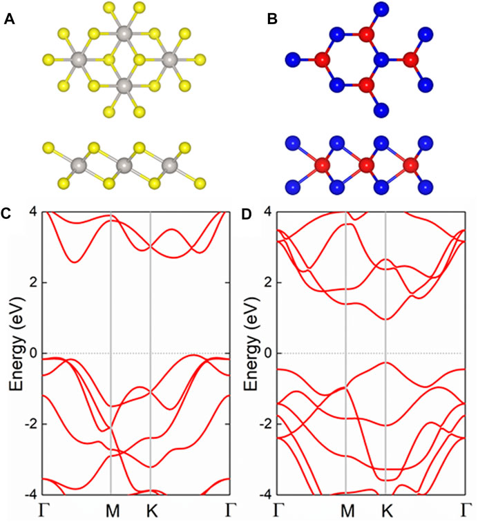
FIGURE 1. The (A,B) geometric and (C,D) band structures of the pristine (A,C) PtS2 and (B,D) MoTe2 monolayers; the yellow, gray, red, and blue balls represent S, Pt, Mo, and Te atoms, respectively; the Fermi level is expressed as 0 using gray dash line.
The PtS2/MoTe2 heterostructure can be constructed by six different configurations considering the high symmetry, named PM-1, PM-2, PM-3, PM-4, PM-5, and PM-6 styles. To decide the most stable staking structure, the binding energy of these different configurations are calculated, and the lowest binding energy is about −28.10 meV Å−2 for PM-6 stacking style, suggesting the van der Waals (vdW) forces between the interface of the PtS2/MoTe2 heterostructure (Chen et al., 2013). The obtained bond length of the Pt−S and Mo−Te in the PtS2/MoTe2 heterostructure are 2.39 and 2.73 Å, which is almost the same as that of the original single-layer material, further demonstrating the vdW interaction. Moreover, the interlayer height (Hi) shown in Figure 2A of the PtS2/MoTe2 vdW heterostructure with PM-6 stacking style is calculated by 2.87 Å. Besides, the following obtained works are based on such PM-6 stacking style.
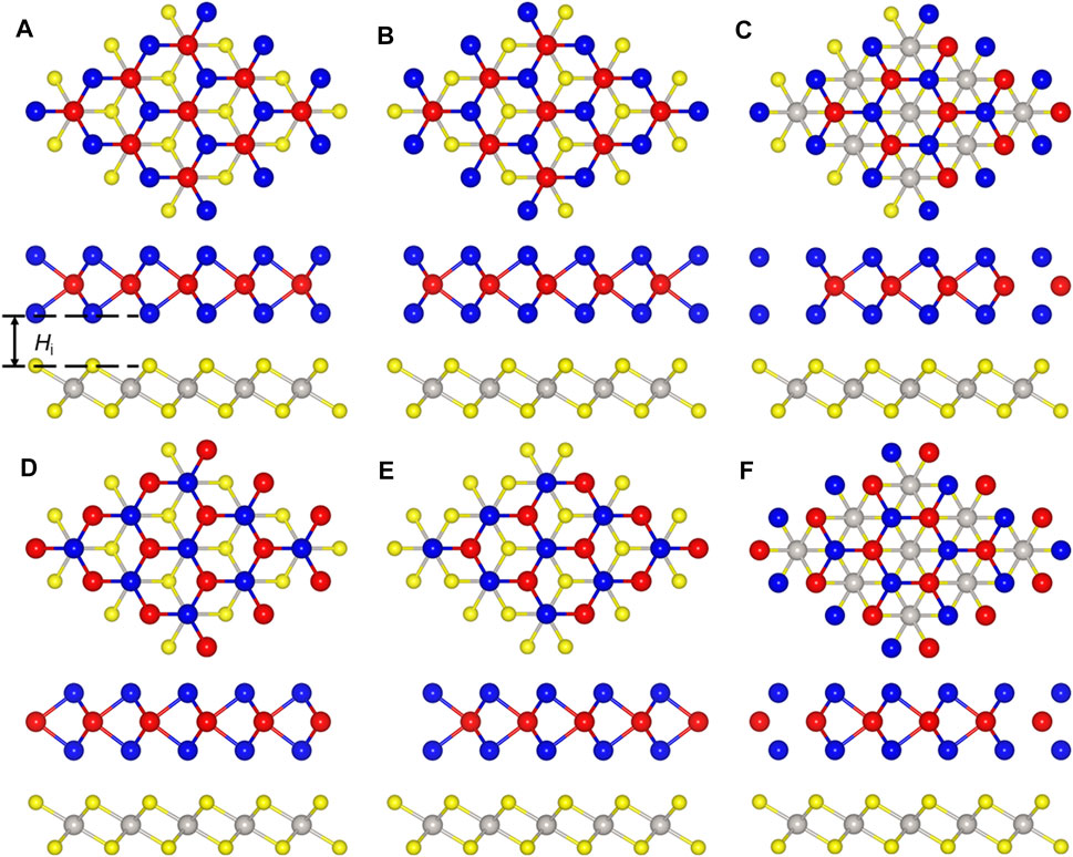
FIGURE 2. The stacking styles of the PtS2/MoTe2 heterostructure constructed by (A) PM-1, (B) PM-2, (C) PM-3, (D) PM-4, (E) PM-5, and (F) PM-6, respectively.
The projected band structure of the PtS2/MoTe2 vdW heterostructure are calculated in Figure 3A, which shows that the CBM and the VBM of the heterostructure are contributed by the PtS2 and MoTe2 monolayers, respectively, suggesting an intrinsic type-II band structure. One can see that the PtS2/MoTe2 vdW heterostructure also is a semiconductor by an indirect bandgap of 1.26 eV that the CBM is located between the Γ and M points, while the CBM exists at K point. Besides, the obtained band-resolved charge densities, explained by Figure 3B, of the PtS2/MoTe2 vdW heterostructure can further demonstrate the different layered contribution to CBM and VBM.
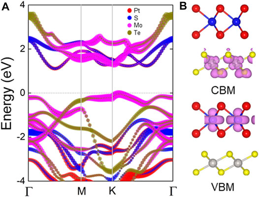
FIGURE 3. (A) The HSE method obtained projected band structure and the (B) band-resolved charge densities of the PtS2/MoTe2 vdW heterostructure; the Fermi level is expressed as 0 using gray dash line.
The type-II band structure of the PtS2/MoTe2 vdW heterostructure can provide the ability to separate the photogenerated electrons (PE) and the holes used as a photocatalyst for water splitting. As shown in Figure 4A, the PtS2/MoTe2 vdW heterostructure takes in the energy of the photon larger than the bandgap of the PtS2 and MoTe2 layers; the PE are excited by the CB of the PtS2 and MoTe2 layers, and thus, the photogenerated holes (PH) stay at the VB at the same time. Then, the PE at the CB of the MoTe2 layer will move to the CB of the PtS2 layer because of the promoting of the conduction band offset, named CBO in Figure 4A. Similarly, the PH at the PtS2 layer also can transfer to the VB of the MoTe2 layer by the development of the valence band offset, denoted by VBO in Figure 4A. Therefore, the PEs are continuously promoted from the CB of the MoTe2 layer to PtS2 layer, while the PHs keep moving from the VB of the PtS2 layer to the MoTe2 layer under continuous solar photodynamic, which induces a PE and PH circulating flow (Wang et al., 2018b).
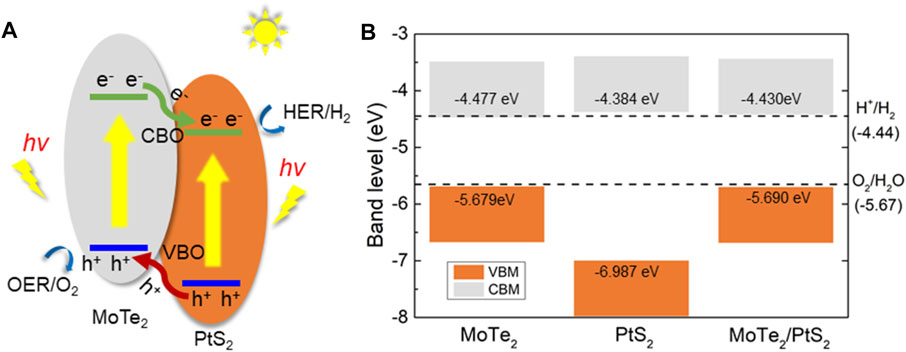
FIGURE 4. (A) The photogenerated charges migration path and (B) the band alignment of the PtS2/MoTe2 vdW heterostructure.
Furthermore, the band edge positions of the PtS2/MoTe2 vdW heterostructure is also calculated in Figure 4B to investigate the photocatalytic driving potential for water splitting. At pH 0, the standard potential energy of the HER and the OER are −4.44 and −5.67 eV, respectively (Wang et al., 2018a). The obtained band alignment of the monolayered PtS2, MoTe2, and the PtS2/MoTe2 vdW heterostructure is demonstrated by Figure 4B, which shows that the monolayered PtS2 and the PtS2/MoTe2 vdW heterostructure have suitable band edge positions to induce the HER and OER at pH 0. However, the PtS2 cannot separate the PE and PH compared with the type-II band structure in the PtS2/MoTe2 vdW heterostructure. Thus, the PtS2/MoTe2 vdW heterostructure can be considered as a potential photocatalyst to decompose the water.
The interfacial performances of the PtS2/MoTe2 vdW heterostructure are assessed by charge density difference (Δρ) and the potential. The charge density difference is calculated by Bader charge analysis (Tang et al., 2009; Henkelman et al., 2006), shown in the inset of Figure 5; the cyan and yellow marks denote the taking and giving of electrons, suggesting that the PtS2 and MoTe2 monolayers act as receivers and donors, respectively. Besides, the obtained charge transfer between the PtS2 and MoTe2 vdW heterostructure is 0.047 electrons. Furthermore, such charge transfer also can induce a potential drop (ΔV) across the PtS2/MoTe2 vdW heterostructure interface, explained by Figure 5. From the PtS2 layer to the MoTe2 layer, the potential decreases by 4.672 eV, which is higher than that in arsenene/GaS (4.215 eV) (Li et al., 2021), AlN/Zr2CO2 (0.663 eV) (Ren et al., 2021c), and Hf2CO2/GaN (3.752 eV) (Ren et al., 2021d) heterostructures. It is worth noting that the potential drop also can provide decent assistance in the process of the separation of photogenerated charges (Wang et al., 2018b).
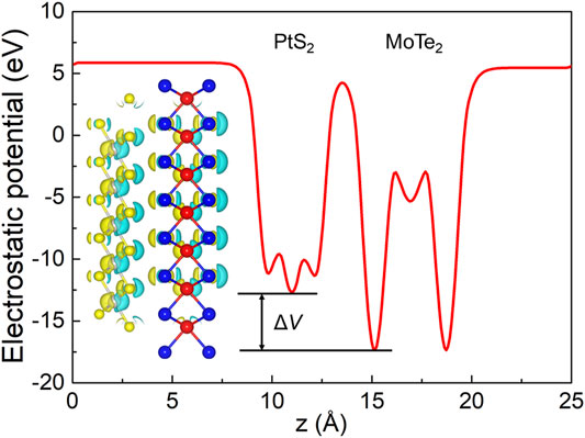
FIGURE 5. The potential drop between the interface of the PtS2/MoTe2 vdW heterostructure; the inset represents the charge density. The isosurface lever was set at 0.015|e|.
Used as a photocatalyst for water splitting, light absorption capacity also has a vital role. The light absorption properties of the monolayered PtS2, MoTe2, and the PtS2/MoTe2 vdW heterostructure are evaluated and shown in Figure 6. The PtS2/MoTe2 vdW heterostructure obviously can improve the optical ability of the monolayered PtS2, MoTe2 in ultraviolet and visible regions. In the visible wavelength range, the absorption peaks of the PtS2 and MoTe2 monolayers and the PtS2/MoTe2 vdW heterostructure are obtained at 4.70 × 10⁵, 2.90 × 10⁵, and 2.57 × 105 cm−1 with wavelengths of 384, 505, and 531 nm, respectively. It is worth noting that MoTe2 monolayer and the tS2/MoTe2 vdW heterostructure possess another absorption peak at 1.53 × 10⁵ and 6.82 × 105 cm−1 with wavelengths of 650 and 380 nm, respectively. The results show that the PtS2 and MoTe2 monolayers and the PtS2/MoTe2 vdW heterostructure have excellent optical performances, which is higher than other reported 2D heterostructures, such as WSSe/Mg(OH)2 (4.295 × 105 cm−1) (Lou et al., 2021), arsenene/GaSe (5.868 × 105 cm−1) (Li et al., 2021), etc.
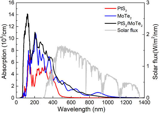
FIGURE 6. The calculated optical absorption spectrum of the monolayered PtS2, MoTe2, and PtS2/MoTe2 vdW heterostructure.
Conclusions
Using DFT calculations, the structural and electronic nature of the monolayered PtS2 and MoTe2 are investigated as semiconductors. Then, the PtS2/MoTe2 heterostructure is constructed by vdW interactions, also showing a type-II band alignment to prevent the PE and PH from recombining. More importantly, the PtS2/MoTe2 vdW heterostructure possesses desirable band edge positions to boost the HER and OER in the PtS2 and MoTe2 layers, respectively. In the PtS2/MoTe2 vdW heterostructure, the PtS2 layer obtains 0.047 electrons from the MoTe2 layer, which induces a 4.672 eV potential drop. Furthermore, all these monolayered PtS2 and MoTe2 and the PtS2/MoTe2 vdW heterostructure show excellent optical properties; particularly, the PtS2/MoTe2 vdW heterostructure suggests a novel light absorption performance in the visible range, revealing the potential application such as new energy vehicle fuel cell photocatalyst.
Data Availability Statement
The raw data supporting the conclusions of this article will be made available by the authors, without undue reservation.
Author Contributions
All authors listed have made a substantial, direct, and intellectual contribution to the work and approved it for publication.
Conflict of Interest
The authors declare that the research was conducted in the absence of any commercial or financial relationships that could be construed as a potential conflict of interest.
Publisher’s Note
All claims expressed in this article are solely those of the authors and do not necessarily represent those of their affiliated organizations or those of the publisher, the editors, and the reviewers. Any product that may be evaluated in this article, or claim that may be made by its manufacturer, is not guaranteed or endorsed by the publisher.
Acknowledgments
The authors thank the Natural Science Foundation Project of Science and Technology Department of Zhejiang Province (Grant No.LZY21E060002), Scientific Research Project of Education Department of Zhejiang Province (Grant No.Y201840751), and Basic Research Fund Project of Colleges and Universities in Zhejiang Province (Grant No.19YQ24).
References
Capelle, K. (2006). A Bird's-Eye View of Density-Functional Theory. Braz. J. Phys. 36, 1318–1343. doi:10.1590/s0103-97332006000700035
Carmo, M., Fritz, D. L., Mergel, J., and Stolten, D. (2013). A Comprehensive Review on PEM Water Electrolysis. Int. J. Hydrogen Energ. 38, 4901–4934. doi:10.1016/j.ijhydene.2013.01.151
Chen, X., Tian, F., Persson, C., Duan, W., and Chen, N.-X. (2013). Interlayer Interactions in Graphites. Sci. Rep. 3, 3046. doi:10.1038/srep03046
Conan, A., Bonnet, A., Amrouche, A., and Spiesser, M. (1984). Semiconducting Properties and Band Structure of MoTe2 Single Crystals. J. Phys. France 45, 459–465. doi:10.1051/jphys:01984004503045900
Dincer, I., and Acar, C. (2015). Review and Evaluation of Hydrogen Production Methods for Better Sustainability. Int. J. Hydrogen Energ. 40, 11094–11111. doi:10.1016/j.ijhydene.2014.12.035
Fujishima, A., and Honda, K. (1972). Electrochemical Photolysis of Water at a Semiconductor Electrode. Nature 238, 37–38. doi:10.1038/238037a0
Geim, A. K., and Novoselov, K. S. (2007). The Rise of Graphene. Nat. Mater 6, 183–191. doi:10.1038/nmat1849
Henkelman, G., Arnaldsson, A., and Jónsson, H. (2006). A Fast and Robust Algorithm for Bader Decomposition of Charge Density. Comput. Mater. Sci. 36, 354–360. doi:10.1016/j.commatsci.2005.04.010
Hernández-Alonso, M. D., Fresno, F., Suárez, S., and Coronado, J. M. (2009). Development of Alternative Photocatalysts to TiO2: Challenges and Opportunities. Energ. Environ. Sci. 2, 1231. doi:10.1039/b907933e
Heyd, J., Peralta, J. E., Scuseria, G. E., and Martin, R. L. (2005). Energy Band Gaps and Lattice Parameters Evaluated with the Heyd-Scuseria-Ernzerhof Screened Hybrid Functional. J. Chem. Phys. 123, 174101. doi:10.1063/1.2085170
Kresse, G., and Furthmüller, J. (1996). Efficient Iterative Schemes Forab Initiototal-Energy Calculations Using a Plane-Wave Basis Set. Phys. Rev. B 54, 11169–11186. doi:10.1103/physrevb.54.11169
Kresse, G., and Joubert, D. (1999). From Ultrasoft Pseudopotentials to the Projector Augmented-Wave Method. Phys. Rev. B 59, 1758–1775. doi:10.1103/physrevb.59.1758
Li, J., Huang, Z., Ke, W., Yu, J., Ren, K., and Dong, Z. (2021). High solar-to-hydrogen efficiency in Arsenene/GaX (X = S, Se) van der Waals heterostructure for photocatalytic water splitting. J. Alloys Compd. 866, 158774. doi:10.1016/j.jallcom.2021.158774
Long, M., Liu, E., Wang, P., Gao, A., Xia, H., Luo, W., et al. (2016). Broadband Photovoltaic Detectors Based on an Atomically Thin Heterostructure. Nano Lett. 16, 2254–2259. doi:10.1021/acs.nanolett.5b04538
Lou, J., Ren, K., Huang, Z., Huo, W., Zhu, Z., and Yu, J. (2021). Electronic and Optical Properties of Two-Dimensional Heterostructures Based on Janus XSSe (X = Mo, W) and Mg(OH)2: a First Principles Investigation. RSC Adv. 11, 29576–29584. doi:10.1039/d1ra05521f
Luo, Y., Wang, S., Ren, K., Chou, J.-P., Yu, J., Sun, Z., et al. (2019). Transition-metal dichalcogenides/Mg(OH)2 van der Waals heterostructures as promising water-splitting photocatalysts: a first-principles study. Phys. Chem. Chem. Phys. 21, 1791–1796. doi:10.1039/c8cp06960c
Moniz, S. J. A., Shevlin, S. A., Martin, D. J., Guo, Z.-X., and Tang, J. (2015). Visible-light Driven Heterojunction Photocatalysts for Water Splitting - a Critical Review. Energy Environ. Sci. 8, 731–759. doi:10.1039/c4ee03271c
Nguyen, C. V., Bui, H. D., Nguyen, T. D., and Pham, K. D. (2019). Controlling electronic properties of PtS2/InSe van der Waals heterostructure via external electric field and vertical strain. Chem. Phys. Lett. 724, 1–7. doi:10.1016/j.cplett.2019.03.048
Ni, M., Leung, D. Y. C., and Leung, M. K. H. (2007). A Review on Reforming Bio-Ethanol for Hydrogen Production. Int. J. Hydrogen Energ. 32, 3238–3247. doi:10.1016/j.ijhydene.2007.04.038
Peng, C., Wei, P., Li, X., Liu, Y., Cao, Y., Wang, H., et al. (2018). High Efficiency Photocatalytic Hydrogen Production over Ternary Cu/TiO2@Ti3C2Tx Enabled by Low-Work-Function 2D Titanium Carbide. Nano Energy 53, 97–107. doi:10.1016/j.nanoen.2018.08.040
Perdew, J. P., Burke, K., and Ernzerhof, M. (1996). Generalized Gradient Approximation Made Simple. Phys. Rev. Lett. 77, 3865–3868. doi:10.1103/physrevlett.77.3865
Qu, D., Liu, X., Huang, M., Lee, C., Ahmed, F., Kim, H., et al. (2017). Carrier-Type Modulation and Mobility Improvement of Thin MoTe2. Adv. Mater. 29, 1606433. doi:10.1002/adma.201606433
Ren, K., Zheng, R., Yu, J., Sun, Q., and Li, J. (2021). Band Bending Mechanism in CdO/Arsenene Heterostructure: A Potential Direct Z-Scheme Photocatalyst. Front. Chem. 9, 788813. doi:10.3389/fchem.2021.788813
Ren, K., Liu, X., Chen, S., Cheng, Y., Tang, W., and Zhang, G. (2020). Remarkable Reduction of Interfacial Thermal Resistance in Nanophononic Heterostructures. Adv. Funct. Mater. 30, 2004003. doi:10.1002/adfm.202004003
Ren, K., Shu, H., Huo, W., Cui, Z., Yu, J., and Xu, Y. (2021). Mechanical, Electronic and Optical Properties of a Novel B2P6 Monolayer: Ultrahigh Carrier Mobility and strong Optical Absorption. Phys. Chem. Chem. Phys. 23, 24915–24921. doi:10.1039/d1cp03838a
Ren, K., Sun, M., Luo, Y., Wang, S., Yu, J., and Tang, W. (2019). First-principle Study of Electronic and Optical Properties of Two-Dimensional Materials-Based Heterostructures Based on Transition Metal Dichalcogenides and boron Phosphide. Appl. Surf. Sci. 476, 70–75. doi:10.1016/j.apsusc.2019.01.005
Ren, K., Tang, W., Sun, M., Cai, Y., Cheng, Y., and Zhang, G. (2020). A direct Z-scheme PtS2/arsenene van der Waals heterostructure with high photocatalytic water splitting efficiency. Nanoscale 12, 17281–17289. doi:10.1039/d0nr02286a
Ren, K., Zheng, R., Lou, J., Yu, J., Sun, Q., and Li, J. (2021). Ab Initio Calculations for the Electronic, Interfacial and Optical Properties of Two-Dimensional AlN/Zr2CO2 Heterostructure. Front. Chem. 9, 796695. doi:10.3389/fchem.2021.796695
Ren, K., Zheng, R., Xu, P., Cheng, D., Huo, W., Yu, J., et al. (2021). Electronic and Optical Properties of Atomic-Scale Heterostructure Based on MXene and MN (M = Al, Ga): A DFT Investigation. Nanomaterials 11, 2236. doi:10.3390/nano11092236
Ren, K., Qin, H., Liu, H., Chen, Y., Liu, X., Zhang, G., et al. (2022). Manipulating Interfacial Thermal Conduction of 2D Janus Heterostructure via a Thermo-Mechanical Coupling. Adv. Funct. Mater. 105, 2110846. doi:10.1002/adfm.202110846
Shen, Z., Ren, K., Zheng, R., Huang, Z., Cui, Z., Zheng, Z., et al. (2022). The Thermal and Electronic Properties of the Lateral Janus MoSSe/WSSe Heterostructure. Front. Mater. 9, 838648. doi:10.3389/fmats.2022.838648
Shi, D., Wang, G., Li, C., Shen, X., and Nie, Q. (2017). Preparation and Thermoelectric Properties of MoTe 2 Thin Films by Magnetron Co-sputtering. Vacuum 138, 101–104. doi:10.1016/j.vacuum.2017.01.030
Stoller, M. D., Park, S., Zhu, Y., An, J., and Ruoff, R. S. (2008). Graphene-based Ultracapacitors. Nano Lett. 8, 3498–3502. doi:10.1021/nl802558y
Sun, M., Chou, J.-P., Hu, A., and Schwingenschlögl, U. (2019). Point Defects in Blue Phosphorene. Chem. Mater. 31, 8129–8135. doi:10.1021/acs.chemmater.9b02871
Sun, M., Luo, Y., Yan, Y., and Schwingenschlögl, U. (2021). Ultrahigh Carrier Mobility in the Two-Dimensional Semiconductors B8Si4, B8Ge4, and B8Sn4. Chem. Mater. 33, 6475–6483. doi:10.1021/acs.chemmater.1c01824
Sun, M., and Schwingenschlögl, U. (2020). B2P6: A Two-Dimensional Anisotropic Janus Material with Potential in Photocatalytic Water Splitting and Metal-Ion Batteries. Chem. Mater. 32, 4795–4800. doi:10.1021/acs.chemmater.0c01536
Sun, M., and Schwingenschlögl, U. (2021). Structure Prototype Outperforming MXenes in Stability and Performance in Metal‐Ion Batteries: A High Throughput Study. Adv. Energ. Mater. 11, 2003633. doi:10.1002/aenm.202003633
Tan, H., Fan, Y., Rong, Y., Porter, B., Lau, C. S., Zhou, Y., et al. (2016). Doping Graphene Transistors Using Vertical Stacked Monolayer WS2 Heterostructures Grown by Chemical Vapor Deposition. ACS Appl. Mater. Inter. 8, 1644–1652. doi:10.1021/acsami.5b08295
Tang, W., Sanville, E., and Henkelman, G. (2009). A Grid-Based Bader Analysis Algorithm without Lattice Bias. J. Phys. Condens. Matter 21, 084204. doi:10.1088/0953-8984/21/8/084204
Tsai, M.-L., Su, S.-H., Chang, J.-K., Tsai, D.-S., Chen, C.-H., Wu, C.-I., et al. (2014). Monolayer MoS2 Heterojunction Solar Cells. ACS nano 8, 8317–8322. doi:10.1021/nn502776h
Wang, B.-J., Li, X.-H., Cai, X.-L., Yu, W.-Y., Zhang, L.-W., Zhao, R.-Q., et al. (2018). Blue Phosphorus/Mg(OH)2 van der Waals Heterostructures as Promising Visible-Light Photocatalysts for Water Splitting. J. Phys. Chem. C 122, 7075–7080. doi:10.1021/acs.jpcc.7b12408
Wang, B., Wang, X., Wang, P., Kuang, A., Zhou, T., Yuan, H., et al. (2021). Bilayer MoTe2/XS2 (X = Hf,Sn,Zr) Heterostructures with Efficient Carrier Separation and Light Absorption for Photocatalytic Water Splitting into Hydrogen. Appl. Surf. Sci. 544. doi:10.1016/j.apsusc.2020.148842
Wang, G., Gong, L., Li, Z., Wang, B., Zhang, W., Yuan, B., et al. (2020). A Two-Dimensional CdO/CdS Heterostructure Used for Visible Light Photocatalysis. Phys. Chem. Chem. Phys. 22, 9587–9592. doi:10.1039/d0cp00876a
Wang, G., Li, Z., Wu, W., Guo, H., Chen, C., Yuan, H., et al. (2020). A Two-Dimensional H-Bn/c2n Heterostructure as a Promising Metal-free Photocatalyst for Overall Water-Splitting. Phys. Chem. Chem. Phys. 22, 24446–24454. doi:10.1039/d0cp03925j
Wang, G., Zhang, L., Li, Y., Zhao, W., Kuang, A., Li, Y., et al. (2020). Biaxial Strain Tunable Photocatalytic Properties of 2D ZnO/GeC Heterostructure. J. Phys. D: Appl. Phys. 53, 015104. doi:10.1088/1361-6463/ab440e
Wang, G., Zhi, Y., Bo, M., Xiao, S., Li, Y., Zhao, W., et al. (2020). 2D Hexagonal Boron Nitride/Cadmium Sulfide Heterostructure as a Promising Water‐Splitting Photocatalyst. Phys. Status Solidi B 257, 1900431. doi:10.1002/pssb.201900431
Wang, H., Zhang, L., Chen, Z., Hu, J., Li, S., Wang, Z., et al. (2014). Semiconductor Heterojunction Photocatalysts: Design, Construction, and Photocatalytic Performances. Chem. Soc. Rev. 43, 5234–5244. doi:10.1039/c4cs00126e
Wang, S., Tian, H., Ren, C., Yu, J., and Sun, M. (2018). Electronic and Optical Properties of Heterostructures Based on Transition Metal Dichalcogenides and Graphene-like Zinc Oxide. Sci. Rep. 8, 12009. doi:10.1038/s41598-018-30614-3
Wang, S., Wang, X., and Warner, J. H. (2015). All Chemical Vapor Deposition Growth of MoS2:h-BN Vertical van der Waals Heterostructures. ACS nano 9, 5246–5254. doi:10.1021/acsnano.5b00655
Zhao, D., Xie, S., Wang, Y., Zhu, H., Chen, L., Sun, Q., et al. (2019). Synthesis of Large-Scale Few-Layer PtS2 Films by Chemical Vapor Deposition. AIP Adv. 9, 025225. doi:10.1063/1.5086447
Keywords: two-dimensional, heterostructure, photocatalyst, type-II band structure, water splitting
Citation: Shao C, Ren K, Huang Z, Yang J and Cui Z (2022) Two-Dimensional PtS2/MoTe2 van der Waals Heterostructure: An Efficient Potential Photocatalyst for Water Splitting. Front. Chem. 10:847319. doi: 10.3389/fchem.2022.847319
Received: 02 January 2022; Accepted: 10 January 2022;
Published: 14 February 2022.
Edited by:
Guangzhao Wang, Yangtze Normal University, ChinaCopyright © 2022 Shao, Ren, Huang, Yang and Cui. This is an open-access article distributed under the terms of the Creative Commons Attribution License (CC BY). The use, distribution or reproduction in other forums is permitted, provided the original author(s) and the copyright owner(s) are credited and that the original publication in this journal is cited, in accordance with accepted academic practice. No use, distribution or reproduction is permitted which does not comply with these terms.
*Correspondence: Kai Ren, a2FpcmVuQG5qZnUuZWR1LmNu; Zhaoming Huang, amltbXltYWN5QDE2My5jb20=
 Changqing Shao1
 Kai Ren