- 1School of Physics and Materials Science Nanchang University, Nanchang, China
- 2School of Physics and Electronic Engineering, Jiangsu University, Zhenjiang, China
- 3College of Information Science and Technology, Nanjing Forestry University, Nanjing, China
Two-dimensional antiferromagnetic semiconductors have triggered significant attention due to their unique physical properties and broad application. Based on first-principles calculations, a novel two-dimensional (2D) antiferromagnetic material MnSi2N4 monolayer is predicted. The calculation results show that the two-dimensional MnSi2N4 prefers an antiferromagnetic state with a small band gap of 0.26 eV. MnSi2N4 has strong antiferromagnetic coupling which can be effectively tuned under strain. Interestingly, the MnSi2N4 monolayer exhibits a half-metallic ferromagnetic properties under an external magnetic field, in which the spin-up electronic state displays a metallic property, while the spin-down electronic state exhibits a semiconducting characteristic. Therefore, 100% spin polarization can be achieved. Two-dimensional MnSi2N4 monolayer has potential application in the field of high-density information storage and spintronic devices.
Introduction
In 2004, the successfully prepared graphene opened a new era of two-dimensional materials (Novoselov et al., 2004). Subsequently, numerous new systems have already been discovered, greatly promoting the development of the two-dimensional material family. Two-dimensional materials have a wide variety of electronic properties, including metallic, semi-metallic, semiconducting and insulating properties. For example, 1H-MoS2 is a semiconductor with a direct band gap, 1T phase MoS2 is a metal, while 1T’ phase MoS2 is semimetal (Hung et al., 2018). In addition, hexagonal boron nitride (h-BN) shows insulating properties (Liu et al., 2003), and graphene is semimetal (Sheng et al., 2019). However, many 2D materials lack intrinsic magnetism, such as graphene and MoS2, which motivates researchers to induce magnetism through defect engineering, adsorption or insertion of magnetic atoms. However, these schemes are difficult to construct stable long-range magnetic order. Therefore, two-dimensional intrinsic ferromagnetic materials have aroused tremendous attention.
According to Mermin-Wagner theory, the long-range magnetic order is predicted to be unstable in 2D material and can be easily destroyed by thermal fluctuations (Mermin and Wagner, 1966). Until 2017, the magnetism in the two-dimensional material CrI3 at the monolayer limit was observed experimentally (Gong et al., 2017; Huang et al., 2017). Hereafter, more 2D magnetic materials have been found, such as Fe3GeTe2 (Xian et al., 2022), FePS3 (Lee et al., 2016) and VSe2 (Bonilla et al., 2018). Two-dimensional magnetic materials possess a wide variety of excellent physical properties. For instance, monolayer magnetic metal materials have been widely used as electrodes in electronic devices, such as Fe3GeTe2 based van der Waals tunnel junctions (O’Hara et al., 2018). Furthermore, magnetic tunnel junction with antimagnetic semiconductor CrI3 tunnel barrier has been reported to possess a giant magnetoresistance effect due to the significant difference of energy band in the ferromagnetic and antiferromagnetic states (Song et al., 2018), which has achieved a huge breakthrough in spintronic devices. Hence antiferromagnetic semiconductor materials have become a hot research topic because of their novel band characteristics. However, such materials are very rare, the prediction of new antiferromagnetic semiconductor materials becomes the key to the development of spintronic devices.
In this paper, the electronic structure and magnetic properties of monolayer MnSi2N4 are explored based on first-principles calculations. The results demonstrate that 2D MnSi2N4 is a stable antiferromagnetic semiconductor in which the ground state is an antiferromagnetic state. The large magnetic exchange parameter indicates a strong antiferromagnetic coupling between the magnetic Mn atoms. When an external magnetic field is applied, the MnSi2N4 monolayer turns into a half-metal with a magnetic state transition from an antiferromagnetic state to a ferromagnetic state. In which the spin-up electronic state displays a metallic nature, while the spin-down electronic state exhibits a semiconducting feature. Therefore, the MnSi2N4 monolayer has great application prospects in spintronics and nanosensors.
Computational details
All calculations were conducted using the Vienna ab initio simulation package (VASP) (Kresse and Furthmuller, 1996; Kresse and Joubert, 1999). The projection plane wave (PAW) method was adopted to describe the interaction between ions and electrons (Blöchl, 1994). The cutoff energy is set as 500 eV. The generalized gradient approximation (GGA) of the form Perdew–Burke–Ernzerhof (PBE) was employed to describe the exchange correlation (Perdew et al., 1996). The convergence criteria for electronic iteration and ionic relaxation were 10–6 eV and 0.001 eV/Å, respectively. An 18 Å vacuum layer was added in the out plane direction of the monolayer MnSi2N4 to eliminate interlayer interactions. The Brillouin zone was sampled with a 13 × 13 × 1 k-point mesh. Due to the strong correlation effect of Mn atoms, the DFT + U method proposed by Dudarev et al. (Dudarev et al., 1998) was adopted, and the effective parameter Ueff was set to 3.9 eV (Wang et al., 2006; Jain et al., 2011; Ling and Mizuno, 2012; Togo and Tanaka, 2015). The phonon spectrum of monolayer MnSi2N4 was calculated by the PHONONPY software (Togoet al., 2015) using a 5 × 5 supercell.
Results and discussion
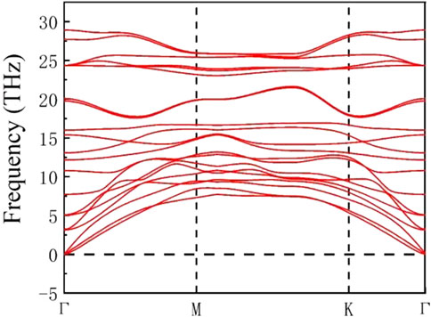
Similar to the two-dimensional MoSi2N4, the monolayer MnSi2N4 is a two-dimensional material with a hexagonal lattice structure and D3h point group as shown in Figure 1. MnSi2N4 monolayer consists of seven atomic layers stacked with the order N-Si-N-Mn-N-Si-N, which can be regarded as a 1H-phase MnN2 triple-layer sandwiched between two buckled N-Si layers. The lattice constant of unit cell is 2.88Å, the bond length between Mn and N atoms is 2.02 Å and the bond length between Si and N atoms is 1.74 Å.
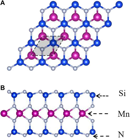
FIGURE 1. Top (A) and side (B) views of MnSi2N4. The balls are highlighted with blue (Si atom), purple (Mn atom) and silvery (N atom). The rhombic unit cells are marked with black dashed lines.
The cohesive energy of the monolayer MnSi2N4 was evaluated to confirm the stability of monolayer MnSi2N4 using the equation:
Where
The magnetic properties of monolayer MnSi2N4 were investigated. We first determined the ground-state magnetic ordering with two possible magnetic order ferromagnetic (FM) and antiferromagnetic (AFM) states. The total energies of the AFM and FM phases of MnSi2N4 are -218.650eV and -217.658 eV, respectively. The energy of the AFM state is lower than that of the FM state, hence MnSi2N4 has an AFM ground state. The AFM order in monolayer MnSi2N4 sourced from the superexchange interactions between two magnetic atoms bridged by nonmetal atoms, following the Goodenough-Kanamori rules (Goodenough, 1955; Kanamori, 1959). In this case, the net magnetic moment is zero and the four Mn atoms in the supercell have an antiparallel magnetic state along with the same value of magnetic moments (3.05 μB). The spin-polarized charge density and the schematic diagram for FM and AFM order are plotted in Figure 3. The spin-polarized charge density map shows that Mn atoms possess an high spin-polarized charge density, while spin-polariztion of N atoms is tiny with small magnetic moments (0.05 μB).
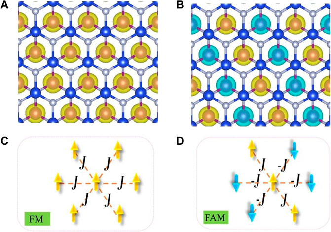
FIGURE 3. (A,B) spin-polarized charge densities of the FM and AFM case for MnSi2N4. The yellow and light blue isosurface with an isosurface value of 0.05 e/Bohr3 represent the spin-up and spin-down charge densities, respectively. (C,D) The scheme represents spin orientation of Mn atoms in FM and AFM case.
The electronic properties of AFM states are investigated to further explore potential applications of MnSi2N4. The electronic band structure and density of states (TDOS) are calculated as illustrated in Figure 4. It is clear that MnSi2N4 exhibits indirect semiconducting property without band cross Fermi level, which is different from nonmagnetic direct bandgap semiconductor MoSi2N4 monolayer (Yuan et al., 2022). The conduction band minimum (CBM) and the valence band maximum (VBM) are located at K point and M point, respectively. The band gap is small (0.26 eV). The bands are degenerate and the TDOS is symmetrical for spin-up and spin-down states. Furthermore, no states exist near the Fermi level along with a small energy gap.
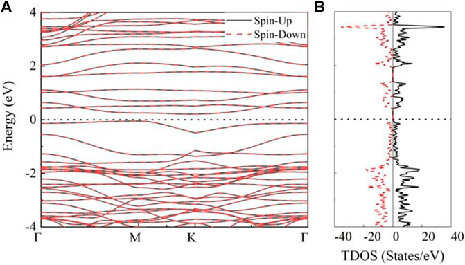
FIGURE 4. (A) The band structures and (B) total density of states (TDOS) of MnSi2N4 monolayer in the AFM states, the spin-up states and spin-down states are represented by the black lines and red dotted lines, respectively.
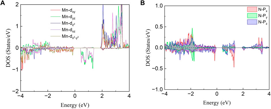
The projected density of states (PDOS) for Mn atom and the nearest neighbor N atom are depicted in Figure 5 to better analyze orbit contribution for electron structure and magnetic properties. One can notice that the density of states for the five 3d orbitals are all asymmetric as shown in Figure 5A, indicating the large spin splitting for an isolated Mn atom. The magnetic moment (3.04 μB/Mn) is mainly dominated by the spin-up (majority-spin) states of d orbitals which is much more than the spin-down electron. For the N atom, the difference in PDOS between the spin-up and spin-down states is not obvious, resulting in a smaller magnetic moment. In addition, the DOS mainly comes from Mn-d and N-p in the energy range from 0.5 to 1.5 eV indicating that the hybridizations between the N-p and Mn-d orbitals are strong.
Furthermore, the ground antiferromagnetic states will transition to ferromagnetic states under an external magnetic field. The band structure and density of states for FM state are depicted in Figure 6. It is clear that the spin-up and spin-down energy bands are not degenerate. The spin-polarized states can be noticed around the Fermi level. In the spin-up channel, several flat bands near the Fermi level existe and the others band display dispersion along Γ–M and K–Γ, which behave as a metal. But for the spin-down channel, a direct bandgap of 2.07 eV is observed with the VBM and CBM located at Γ point. Hence, MnSi2N4 monolayer behaves half-metallic properties in the FM case. The spin polarization is obvious with an asymmetric density of states distribution for spin-up and spin-down states as depicted in Figure 6B. One can find that a peak of spin-up states can be seen near the Fermi level and a large bandgap exists in the spin-down states, which further confirms the metallic behavior for the spin-up states and semiconducting property for spin-down states, respectively. Therefore, the 2D MnSi2N4 in FM state is a half-metal with 100% spin polarization.
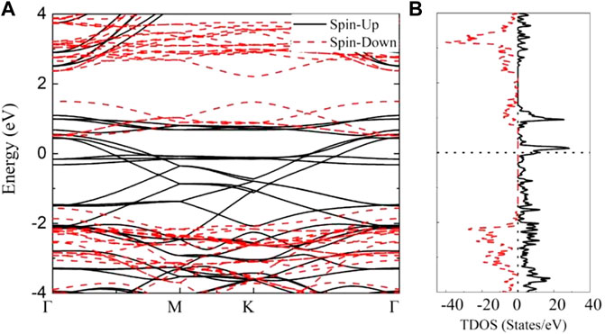
FIGURE 6. (A) The band structures and (B) total density of states (TDOS) of MnSi2N4 in the FM states, the spin-up states and spin-down states are represented by the black lines and red dotted lines, respectively.
Strain is an effective means of manipulating electronic structure and magnetic properties which is widely utilized to modulate the electronic structure and magnetic properties of monolayer system. In this paper, the strain is defined as ε = (a − a0)/a0, where a0 is the relaxed lattice constant in the equilibrium state. The magnetic moment of the Mn atom remains about 3 μB per unit cell under strain. The effective spin Hamiltonian based on the Heisenberg model can be expressed as
where
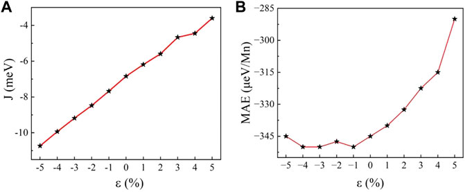
FIGURE 7. (A) Magnetic exchange parameter J and (B) magnetocrystalline anisotropy energy EMAE as a function of strain.
To identify the easy axis of MnSi2N4, we computed the magnetic anisotropy energy (MAE). The MAE of the magnetic crystal is defined as EMAE = Ein-Eout (Webster and Yan, 2018), that is, the energy difference between the in-plane (Ein) and out-of-plane (Eout) of MnSi2N4. For the strain-free monolayer MnSi2N4, the MAE is −345 μeV/Mn atom, indicating that the easy axis of MnSi2N4 prefers in-plane and the spin of the Mn atoms is arranged parallel to the basal plane. The MAE of monolayer MnSi2N4 is mainly derived from Mn atoms since Mn atoms have relatively stronger spin-orbit coupling than other atoms. The MAE is depicted as a function of strain in Figure 7B. When the structure is compressed, this value fluctuates around −350 μeV/Mn, hence the effect of compressive strain on MAE is not obvious. While MAE increases significantly with increasing tensile strain. MAE changes from -345 μeV/Mn to −290 μeV/Mn under the 5% tensile strain.
Conclusion
The electronic and magnetic properties of monolayer MnSi2N4 are explored based on first-principles calculations. Monolayer MnSi2N4 is an intrinsic antiferromagnetic semiconductor with a small indirect band gap (0.26 eV). The MnSi2N4 has strong antiferromagnetic coupling along with strong in-plane magnetocrystalline anisotropy energy (−345 μeV/Mn). Furthermore, the MnSi2N4 monolayer exhibits half-metallic properties with a metallic spin-up state and a semiconducting spin-down state. The effect of biaxial strain on magnetism is also investigated. The magnetic exchange parameter J and MAE increase with biaxial tensile strain. The tunable magnetic properties may enrich the 2D antiferromagnets community and stimulate potential applications in spintronic devices.
Data availability statement
The original contributions presented in the study are included in the article/Supplementary Material, further inquiries can be directed to the corresponding author.
Author contributions
DC and ZJ: Conceptualization, methodology, software; JY and J-JH: Investigation, Formal analysis, Visualization; JZ and YG: Formal analysis, Data Curation; DC and YT: Writing—original draft preparation; JY: Supervision, Writing—review and editing.
Funding
Financial support was received from the National Natural Science Foundation of China (NSFC12004142 and NSFC12264026), and Natural Science Funds for Colleges and Universities in Jiangsu Province (20KJB140017).
Conflict of interest
The authors declare that the research was conducted in the absence of any commercial or financial relationships that could be construed as a potential conflict of interest.
Publisher’s note
All claims expressed in this article are solely those of the authors and do not necessarily represent those of their affiliated organizations, or those of the publisher, the editors and the reviewers. Any product that may be evaluated in this article, or claim that may be made by its manufacturer, is not guaranteed or endorsed by the publisher.
References
Bafekry, A., Faraji, M., Stampfl, C., Abdolhosseini Sarsari, I., Abdollahzadeh Ziabari, A., Hieu, N. N., et al. (2021). Band-gap engineering, magnetic behavior and Dirac-semimetal character in the MoSi2N4 nanoribbon with armchair and zigzag edges. J. Phys. D. Appl. Phys. 55 (3), 035301. doi:10.1088/1361-6463/ac2cab
Blöchl, P. E. (1994). Projector augmented-wave method. Phys. Rev. B 50 (24), 17953–17979. doi:10.1103/PhysRevB.50.17953
Bonilla, M., Kolekar, S., Ma, Y., Diaz, H. C., Kalappattil, V., Das, R., et al. (2018). Strong room-temperature ferromagnetism in VSe2 monolayers on van der Waals substrates. Nat. Nanotechnol. 13, 289–293. doi:10.1038/s41565-018-0063-9
Canton-Vitoria, R., Sayed-Ahmad-Baraza, Y., Humbert, B., Arenal, R., Ewels, C., and Tagmatarchis, N. (2020). Pyrene coating transition metal disulfides as protection from photooxidation and environmental aging. Nanomaterials 10 (2), 363. doi:10.3390/nano10020363
Dudarev, S. L., Botton, G. A., Savrasov, S. Y., Humphreys, C. J., and Sutton, A. P. (1998). Electron-energy-loss spectra and the structural stability of nickel oxide: An LSDA+ U study. Phys. Rev. B 57 (3), 1505–1509. doi:10.1103/PhysRevB.57.1505
Gong, C., Li, L., Li, Z., Ji, H., Stern, A., Xia, Y., et al. (2017). Discovery of intrinsic ferromagnetism in two-dimensional van der Waals crystals. Nature 546 (7657), 265–269. doi:10.1038/nature22060
Goodenough, J. B. (1955). Theory of the role of covalence in the perovskite-type manganites [La, M (II)] MnO3. Phys. Rev. 100 (2), 564–573. doi:10.1103/PhysRev.100.564
Huang, B., Clark, G., Navarro-Moratalla, E., Klein, D. R., Cheng, R., Seyler, K. L., et al. (2017). Layer-dependent ferromagnetism in a van der Waals crystal down to the monolayer limit. Nature 546 (7657), 270–273. doi:10.1038/nature22391
Hung, N. T., Nugraha, A. R. T., and Saito, R. (2018). Two-dimensional MoS2 electromechanical actuators. J. Phys. D. Appl. Phys. 51 (7), 075306. doi:10.1088/1361-6463/aaa68f
Jain, A., Hautier, G., Moore, C. J., Ping Ong, S., Fischer, C. C., Mueller, T., et al. (2011). A high-throughput infrastructure for density functional theory calculations. Comput. Mat. Sci. 50 (8), 2295–2310. doi:10.1016/j.commatsci.2011.02.023
Kan, M., Zhou, J., Sun, Q., Kawazoe, Y., and Jena, P. (2013). The intrinsic ferromagnetism in a MnO2 monolayer. J. Phys. Chem. Lett. 4 (20), 3382–3386. doi:10.1021/jz4017848
Kanamori, J. (1959). Superexchange interaction and symmetry properties of electron orbitals. J. Phys. Chem. Solids 10 (2-3), 87–98. doi:10.1016/0022-3697(59)90061-7
Kresse, G., and Furthmüller, J. (1996). Efficient iterative schemes for ab initio total-energy calculations using a plane-wave basis set. Phys. Rev. B 54 (16), 11169–11186. doi:10.1103/PhysRevB.54.11169
Kresse, G., and Joubert, D. (1999). From ultrasoft pseudopotentials to the projector augmented-wave method. Phys. Rev. B 59 (3), 1758–1775. doi:10.1103/PhysRevB.59.1758
Lee, J. U., Lee, S., Ryoo, J. H., Kang, S., Kim, T. Y., Kim, P., et al. (2016). Ising-type magnetic ordering in atomically thin FePS3. Nano Lett. 16 (12), 7433–7438. doi:10.1021/acs.nanolett.6b03052
Ling, C., and Mizuno, F. (2012). Capture lithium in αMnO2: Insights from first principles. Chem. Mat. 24 (20), 3943–3951. doi:10.1021/cm302347j
Liu, L., Feng, Y. P., and Shen, Z. X. (2003). Structural and electronic properties of h-BN. Phys. Rev. B 68 (10), 104102. doi:10.1103/PhysRevB.68.104102
Mermin, N. D., and Wagner, H. (1966). Absence of ferromagnetism or antiferromagnetism in one-or two-dimensional isotropic Heisenberg models. Phys. Rev. Lett. 17 (22), 1133–1136. doi:10.1103/PhysRevLett.17.1133
Novoselov, K. S., Geim, A. K., Morozov, S. V., Jiang, D., Zhang, Y., Dubonos, S. V., et al. (2004). Electric field effect in atomically thin carbon films. Science 306 (5696), 666–669. doi:10.1126/science.1102896
O’Hara, D. J., Zhu, T., Trout, A. H., Ahmed, A. S., Luo, Y. K., Lee, C. H., et al. (2018). Room temperature intrinsic ferromagnetism in epitaxial manganese selenide films in the monolayer limit. Nano Lett. 18 (5), 3125–3131. doi:10.1021/acs.nanolett.8b00683
Perdew, J. P., Burke, K., and Ernzerhof, M. (1996). Generalized gradient approximation made simple. Phys. Rev. Lett. 77 (18), 3865–3868. doi:10.1103/PhysRevLett.77.3865
Sheng, X. L., Chen, C., Liu, H., Chen, Z., Yu, Z. M., Zhao, Y., et al. (2019). Two-dimensional second-order topological insulator in graphdiyne. Phys. Rev. Lett. 123 (25), 256402. doi:10.1103/PhysRevLett.123.256402
Song, T. C., Cai, X., Tu, M. W. Y., Zhang, X., Huang, B., Wilson, N. P., et al. (2018). Giant tunneling magnetoresistance in spin-filter van der Waals heterostructures. Science 360, 1214–1218. doi:10.1126/science.aar4851
Togo, A., and Tanaka, I. (2015). First principles phonon calculations in materials science. Scr. Mat. 108, 1–5. doi:10.1016/j.scriptamat.2015.07.021
Wang, L., Maxisch, T., and Ceder, G. (2006). Oxidation energies of transition metal oxides within theGGA+Uframework. Phys. Rev. B 73 (19), 195107. doi:10.1103/PhysRevB.73.195107
Webster, L., and Yan, J. A. (2018). Strain-tunable magnetic anisotropy in monolayer CrCl3, CrBr3, and CrI3. Phys. Rev. B 98 (14), 144411. doi:10.1103/PhysRevB.98.144411
Xian, J. J., Wang, C., Nie, J. H., Li, R., Han, M., Lin, J., et al. (2022). Spin mapping of intralayer antiferromagnetism and field-induced spin reorientation in monolayer CrTe2. Nat. Commun. 13, 257. doi:10.1038/s41467-021-27834-z
Keywords: two-dimensional materials, antiferromagnetic semiconductor, half metals, electronic properties, biaxial strain
Citation: Chen D, Jiang Z, Tang Y, Zhou J, Gu Y, He J-J and Yuan J (2022) Electrical and magnetic properties of antiferromagnetic semiconductor MnSi2N4 monolayer. Front. Chem. 10:1103704. doi: 10.3389/fchem.2022.1103704
Received: 20 November 2022; Accepted: 28 November 2022;
Published: 08 December 2022.
Edited by:
Guangzhao Wang, Yangtze Normal University, ChinaReviewed by:
Xiaoming Zhang, Hebei University of Technology, ChinaWeikang Wu, Shandong University, China
Copyright © 2022 Chen, Jiang, Tang, Zhou, Gu, He and Yuan. This is an open-access article distributed under the terms of the Creative Commons Attribution License (CC BY). The use, distribution or reproduction in other forums is permitted, provided the original author(s) and the copyright owner(s) are credited and that the original publication in this journal is cited, in accordance with accepted academic practice. No use, distribution or reproduction is permitted which does not comply with these terms.
*Correspondence: Jiaren Yuan, anJ5dWFuQG5jdS5lZHUuY24=
 Dongke Chen
 Zhengyu Jiang2
 Ying Tang
 Jiaren Yuan