
95% of researchers rate our articles as excellent or good
Learn more about the work of our research integrity team to safeguard the quality of each article we publish.
Find out more
ORIGINAL RESEARCH article
Front. Chem. , 13 October 2022
Sec. Inorganic Chemistry
Volume 10 - 2022 | https://doi.org/10.3389/fchem.2022.1046010
 Fangfang Chen1†Dingwen Cao2†Juanjuan Li1
 Yong Yan2
 Di Wu1Cheng Zhang3Lenan Gao1Zhaowei Guo1Shihong Ma1Huihui Yu4*
 Pei Lin1*
Research on elemental 2D materials has been experiencing a renaissance in the past few years. Of particular interest is tellurium (Te), which possesses many exceptional properties for nanoelectronics, photonics, and beyond. Nevertheless, the lack of a scalable approach for the thickness engineering and the local properties modulation remains a major obstacle to unleashing its full device potential. Herein, a solution-processed oxidative etching strategy for post-growth thickness engineering is proposed by leveraging the moderate chemical reactivity of Te. Large-area ultrathin nanosheets with well-preserved morphologies could be readily obtained with appropriate oxidizing agents, such as HNO2, H2O2, and KMnO4. Compared with the conventional physical thinning approaches, this method exhibits critical merits of high efficiency, easy scalability, and the capability of site-specific thickness patterning. The thickness reduction leads to substantially improved gate tunability of field-effect transistors with an enhanced current switching ratio of ∼103, promoting the applications of Te in future logic electronics. The response spectrum of Te phototransistors covers the full range of short-wave infrared wavelength (1–3 μm), and the room-temperature responsivity and detectivity reach 0.96 AW-1 and 2.2 × 10⁹ Jones at the telecom wavelength of 1.55 μm, together with a favorable photocurrent anisotropic ratio of ∼2.9. Our study offers a new approach to tackling the thickness engineering issue for solution-grown Te, which could help realize the full device potential of this emerging p-type 2D material.
Monoelemental two-dimensional (2D) crystals represent a particular category in the 2D materials family because of their unique physicochemical properties (Mannix et al., 2017). Graphene is indisputably the most famous one that has triggered the whole research field. Nevertheless, research on compound 2D materials (e.g., transition metal disulfides, metal halides, and transition metal carbides/nitrides) seems to dominate this area owing to their much larger numbers. With the substantial progress in synthesis technologies, a series of 2D main group elements and transition metals have been experimentally realized over the past few years and reawaken the researcher’s intense interest (Glavin et al., 2020; Fan et al., 2021; Si et al., 2021; Zhou et al., 2021). The elemental 2D materials typically exhibit metallic or semiconducting characteristics with high room-temperature carrier mobility, strong light absorption, and emerging topological properties, enabling potential widespread applications in future electronics, photonics, and energy-related devices (Nevalaita and Koskinen, 2018; Lin et al., 2020; Wu Z et al., 2021; Bat-Erdene et al., 2022). Moreover, the elemental materials bear a distinct advantage over 2D compounds in high-quality synthesis because the dissociation and stoichiometric problems do not exist.
Of particular interest among them is the emerging 2D tellurium (Te) that exhibits an intrinsic p-type transport characteristic and high hole mobility of ∼1,300 cm2·V−1·s−1, offering a new material platform to combine with many n-type 2D crystals for van der Waals (vdW) heterojunction electronics (Huang et al., 2017; Zhu et al., 2017; Wang et al., 2018; Tong et al., 2020; Zhao et al., 2021; Zhang et al., 2022) Besides, the highly-tunable bandgap of Te (∼0.35–1.2 eV) perfectly bridges the gap between semimetals and the widely-studied 2D transition metal disulfides and has unique applications in the short-wave infrared (SWIR) photodetection (Amani et al., 2018; Deckoff-Jones et al., 2019; Chaves et al., 2020; Peng et al., 2021; Ma et al., 2022). In particular, its strong anisotropic lattice structure enables the direct detection of the polarization information of infrared light, which is difficult to realize with the current infrared imaging technology. Generally, Te shares many similar properties with black phosphorus (BP) but has better ambient stability due to its higher oxidation barrier in ambient. Many previous studies have established that the performance of Te-based transistors and detectors hardly degrades over several months, even without any encapsulation (Wang et al., 2018; Tong et al., 2020; Ma et al., 2022).
Despite the versatile synthesis techniques for Te, such as chemical vapor deposition (Huang et al., 2021; Peng et al., 2021; Yang et al., 2022; Zhao et al., 2022), physical vapor deposition (Wang et al., 2014; Tao et al., 2021), and molecular beam epitaxy (Chen et al., 2017; Zheng W et al., 2021), the substrate-free solution approach offers distinct advantages of low temperature (<200°C) and scalability. It has been widely used to prepare monocrystal quasi-2D nanosheets with a lateral size of over 100 μm (Yao et al., 2021a). Nevertheless, due to its special growth mechanism, this method could not easily acquire ultrathin Te by adjusting the synthesis parameters (Londono-Calderon et al., 2020; Li et al., 2021). The hydrothermally-processed 2D crystals using Na2TeO3 and polyvinylpyrrolidone (PVP) as the precursor possess a typical thickness larger than 20 nm, while the Te flakes synthesized by oxidizing tellurium sodium hydride generally have a thickness of 50–170 nm (Wang et al., 2019; Hu et al., 2021). Due to the small bandgap and large carrier density, the thick Te usually exhibits degenerate charge transfer characteristics and a weak gate tuning of drain current at room temperature, limiting its application in logic electronics and optoelectronics.
Te is located between semiconducting selenium and metallic polonium in group VIA of the periodic table. The special electronic configuration endows it with moderate reactivity, allowing properties manipulation by appropriate chemical transformation (Xu et al., 2015). Leveraging this unique characteristic, we present a novel solution-processed oxidative etching method for Te post-growth thickness engineering. Scalable ultrathin Te nanosheets with well-retained morphologies could be easily obtained with appropriate oxidizing agents, such as HNO2, H2O2, and KMnO4. Particularly, thickness patterning is realized when combined with the photolithography technique, which enables the local modulation of material properties and the artificial design of novel device architectures. Field-effect transistors (FETs) fabricated with thinned Te reveals a much-enhanced current ON/OFF ratio of ∼103, promoting their future applications in logic devices. The response spectrum of Te phototransistors covers the full range of SWIR wavelength (λ = 1–3 μm), and the responsivity and detectivity reach 0.96 AW−1 and 2.2 × 10⁹ Jones at the optical communication wavelength of 1.55 μm. Besides, a high photocurrent anisotropic ratio of ∼2.9 is obtained, which ensures the promising application of Te in polarized infrared imaging. Scalable Thickness engineering has been considered a major obstacle for solution-grown Te. Our study offers a new approach to tackling this issue, helping unleash the full device potential of this emerging 2D material.
The synthesis of quasi-2D Te nanosheets starts with dissolving 0.6 g of PVP (Mw 58,000) and 0.11 g of Na2TeO3 in 16 ml of ultrapure water. The mixture was magnetically stirred for 20 min to form a transparent homogeneous solution. 2 ml of ammonia solution (25%–28%, w/w) and 1 ml of hydrazine hydrate (80%, w/w) were then added. After another 1 min of magnetic stirring, the nutrient solution was transferred into a 50 ml hydrothermal reactor. The crystal growth process was performed at 180°C for 4.5 h. The resulting Te nanosheets were centrifuge-washed several times at 5,000 rpm and finally redispersed in the ultrapure water.
An oxidative-etching method with HNO2 was first adopted for post-growth thinning of Te nanosheets. The oxidant solution was prepared by adding 25 mg of sodium nitrite (NaNO2) into 40 ml of dilute hydrochloric acid (HCl, 10 mmol/L). The number of moles of H+ is slightly larger than that of NO2- for the subsequent acid etching process. The thinning was performed by immersing drop-casted Te nanosheets on SiO2/Si substrate into the solution at room temperature (or mixing the oxidant solution with Te redispersion solution). Thickness engineering with other appropriate oxidizing agents, such as H2O2 and KMnO4, and the H2O2 concentration-dependent thinning effect were also investigated.
The FETs and phototransistors were fabricated by transferring Te nanosheets onto the SiO2/p+-Si substrate via a poly (vinyl chloride)-assisted dry transfer method (Wakafuji et al., 2020). The standard electron-beam lithography process was performed to define the source and drain patterns. High-work-function metals Pd/Au (10 nm/50 nm) were evaporated as the contact electrodes.
An optical microscope (SOPTOP-CX40M) was employed to investigate the Te morphologies. The accurate thickness of materials was measured with an atomic force microscope (AFM, Bruker dimension Icon). The transmission electron microscopy (TEM) characterization was performed with a JEM-2100 electron microscope operated at 200 kV. The polarized Raman spectra were taken using the LabRAM HR Evolution Raman system with a 532 nm excitation laser. The room-temperature electrical properties were acquired with a Keithley 4200A-SCS semiconductor parameter analyzer. Power-tunable lasers (980 nm, 1.55 μm, and 3.0 μm wavelength) coupled with optical fiber were used as the illumination source.
The elemental Te typically forms a trigonal lattice structure, which consists of helical chains arranged hexagonally, as shown in Figure 1A (Agapito et al., 2013; Zhu et al., 2017; Qiao et al., 2018). The bonds between neighboring Te atoms on the same chain are covalent, whereas the interaction between chains is considered a mixture of electronic and vdW types (Weidmann and Anderson, 1971). Figure 1B exhibits the optical microscope images of solution-grown Te nanoflakes. It can be found that the length and width could exceed 100 and 30 μm, respectively. The Te crystal structure is determined using TEM and X-ray diffraction (XRD). Figure 1C presents the low- and high-magnification TEM images of an individual Te and corresponding selected area electron diffraction pattern with sharp spots, revealing the high crystallinity of synthetic nanosheets. The calculated interplanar distance of 0.6 nm is consistent with the trigonal-Te (0001) planes, which verifies that the length’s growth direction is c-axis oriented (Wang et al., 2018). The XRD result in Figure 1D matches well with the standard diffraction file JCPDS card (No. 36-1452), further confirming the trigonal structure of Te. The Raman spectrum in Figure 1E shows three sharp characteristic peaks at 91.5 cm−1, 119.9 cm−1, and 139.8 cm−1, corresponding to the E1-TO, A1, and E2 vibrational modes (Pine and Dresselhaus, 1971; Tong et al., 2020; Wang et al., 2022). Lorentzian fitting of these peaks yields a narrow full width at half maximum of 3.6 cm−1, 6.7 cm−1, and 3.2 cm−1, respectively (Supplementary Figure S1). Moreover, angle-resolved Raman spectra were measured to investigate the optical anisotropy properties of Te, as shown in Figure 1F. The intensity anisotropic ratios for E1-TO and A1 vibrational mode (Figures 1G,H) reach 29.4 and 2.1, evidencing its great potential for applications in polarized infrared photodetection (Supplementary Figure S2). The atomic force microscope is employed to measure the material thickness, ranging from about 20 to 120 nm (Supplementary Figure S3). Figure 1I shows an AFM image of a typical Te nanosheet and corresponding cross-section height profile, revealing a thickness of ∼30 nm.
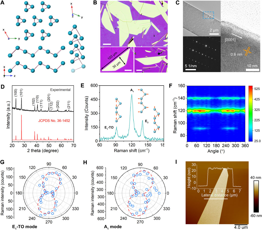
FIGURE 1. Characterizations of the solution-grown 2D Te flakes. (A) Schematic lattice structure of trigonal Te. (B) Optical images of Te nanosheets. The scale bar is 20 μm. (C) Low- and high-magnification TEM images of individual Te and corresponding selected area diffraction pattern, evidencing its single crystallinity and growth direction along the c-axis. (D) XRD pattern of synthetic Te. (E) Raman spectrum that shows characteristic peaks of E1-TO, A1, and E2 vibrational modes. (F) Angle-resolved polarized Raman mapping of Te nanosheet. Polar plots of Raman intensity for (G) E1-TO and (H) A1 mode. (I) AFM image of a typical Te nanosheet, the thickness is ∼30 nm.
The Kelvin probe force microscope (KPFM) measurement was performed to investigate the work function of Te on conductive Au substrate (Supplementary Figure S4B). The result indicates that the average contact potential difference ΔVCPD of Te nanosheet is ∼240 mV larger than Au. Considering the determined work function of ∼5.1 eV for Au, the work function of Te is calculated to be ∼4.86 eV. Moreover, ultraviolet photoelectron spectroscopy (UPS) was also measured (Supplementary Figure S4A). The estimated work function of as-grown Te is ∼4.85 eV, which is consistent with the KPFM results.
A major obstacle in the solution synthesis of Te is that the ultrathin nanosheets with a thickness less than 10 nm cannot be easily derived via tuning synthetic parameters (e.g., temperature, the mole ratio of precursors, synthesis time, etc.) (Wang et al., 2019; Hu et al., 2021). The large material thickness generally results in weak electrostatic tunability of the Te FETs and a high off-state current, which is unfavorable for logic electronics and optoelectronics (Wang et al., 2018; Zhao et al., 2020; Yao et al., 2021b). Despite the excellent ambient stability, the element Te has been demonstrated to possess moderate chemical reactivity (Yang et al., 2015; He et al., 2019). Using this unique characteristic, we propose a solution-processed wet-chemical strategy with the weak oxidizing agent HNO2 for the Te thickness engineering. The standard redox potential of HNO2/NO is ∼0.996 V (vs. standard hydrogen electrode), higher than that of TeO2/Te (0.59 V) (Bockris and Oldfield, 1955; Yang et al., 2018; Zheng B et al., 2021). Therefore, the elemental Te could be oxidized in dilute HNO2 solution, with the generated TeO2 being subsequently etched away by the excess H+, leading to the gradual reduction of material thickness. Figure 2A presents the optical images of an individual Te flake upon in-situ thinning with HNO2 solution for different times, showing an apparent gradual thickness reduction. From the Raman spectra in Figure 2B, it can be found that the A1 and E2 vibrational peaks blueshift with decreasing thickness, which agrees with our previous reports (Yao et al., 2021b). Moreover, the control experiments were carried out with individual NaNO2 and HCl solutions (Supplementary Figure S5). No apparent morphology change could be observed, confirming the thinning effect with HNO2.
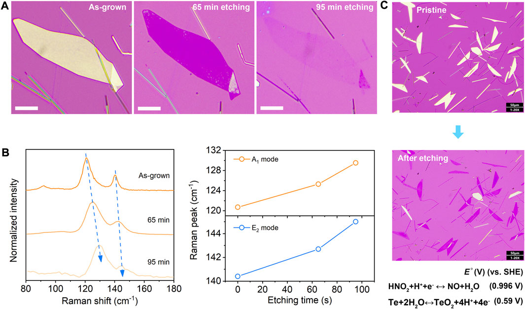
FIGURE 2. Controllable thinning of the Te nanosheets. (A) Optical images of an individual Te flake upon in-situ oxidative etching with HNO2 solution. Scale bar, 10 μm. (B) Corresponding Raman spectra of the Te sample, indicating blueshift of A1 and E2 peaks with thickness reduction. (C) Optical images of Te before and after the wet etching process with HNO2, revealing the capability of scalable thinning.
Compared with the physical thinning approaches such as plasma, focused ion beam, or laser etching (Castellanos-Gomez et al., 2012; Wang et al., 2016; Nan et al., 2019), this method has a distinct advantage of low cost and easy scalability. The large-area ultrathin Te nanosheets could be easily prepared, as shown in Figure 2C. Based on the same rationale, other appropriate oxidizing agents such as H2O2 and KMnO4 are also employed for the thinning process, as demonstrated in Supplementary Figure S6. Ultrathin Te nanosheets with well-retained morphologies and controllable thickness are obtained, revealing the general applicability of this method. It should be noted that under the similar oxidant concentration, the thinning efficiency of H2O2 and KMnO4 is typically higher than HNO2, which is due to the higher standard redox potential. The H2O2 concentration-dependent thinning effect was also explored, and the details are presented in Supplementary Figure S7. Compared with the previously reported post-growth thinning of Te in mixed alkaline and acetone solution (Wang et al., 2018), our approach relies on a different mechanism. Furthermore, it is supposed to have higher thinning efficiency. Ultrathin Te crystals with a thickness smaller than 10 nm could be readily derived within several minutes.
Additionally, due to the mild processing conditions, this approach enables arbitrary site-specific thickness patterning when combined with the conventional photolithography technique (Figure 3A). Figure 3B presents the optical image of Te nanosheet with a “TE” poly (methyl methacrylate) pattern on the surface. The local thinning characteristic is confirmed from the atomic force microscope images after 30 min etching in HNO2, as shown in Figures 3C,D. Figure 3E shows the height profiles of pristine and thinned Te areas. The thickness of pristine Te is measured to be ∼31.5 nm, and the etching depth is ∼16.7 nm. Moreover, the etched areas exhibit relatively uniform thickness and sharp edges, revealing the potential of creating high-resolution patterns with this method. As is known, the electronic structure is strongly thickness-dependent for 2D materials. The artificial thickness patterning offers vast enticing possibilities to locally manipulate the physical properties of Te for designing novel electronics and optoelectronics.
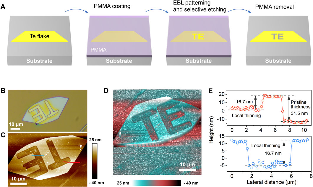
FIGURE 3. (A) Schematic fabrication process for the thickness patterning of Te nanosheet. (B) Optical image of the Te nanosheet with a “TE” photoresist pattern on the surface. (C–D) 2D and 3D AFM images of the locally-thinned Te flake. (E) Height profiles along the blue and red lines in (C), revealing the capability of local thinning with this oxidative etching method.
The thinning effect on the electrical properties of Te FETs is further explored. Figure 4A shows the transfer (Ids-Vg) and output (Ids-Vds) curves of FET fabricated with as-grown Te nanosheet, revealing a typical p-type transport characteristic and favorable room-temperature hole mobility of ∼630 cm2·V−1·s−1 (Supplementary Figure S8). Nevertheless, the ON/OFF ratio is generally less than one order of magnitude, and gate control over the drain current is weak owing to the considerable material thickness and high carrier density. In contrast, the FET with thinned Te channel (Figure 4B) presents significantly improved electrostatic tunability, with the ON/OFF ratio reaching ∼103 at Vg of ± 60 V. Moreover, the ratio is supposed to be further improved by optimizing the device structure, such as employing high-k dielectrics and performing surface passivation. The tunable electrical properties in Te and the feasibility of local thickness engineering provide a versatile approach to fabricating on-demand electronics and optoelectronics. The effect of contact electrodes on the FET properties is also investigated. Figure 4C displays the transfer and output curves of another FET with thinned Te channel and Cr/Au (10 nm/50 nm) electrodes. The thickness of Te is estimated to be thinner than that in Figure 4B from the optical contrast, which should logically present a higher ON/OFF switching ratio. However, the measured ON/OFF ratio is lower. Meanwhile, a more pronounced Schottky contact is observed from the output characteristics. One of the reasons may be that the work function of Cr (∼4.5 eV) is smaller than that of Pd (∼5.2 eV), as schematically displayed in Figure 4D. The resulting larger Schottky barrier height at the Cr/p-Te interface and, thus, large contact resistance restrains the hole transport capabilities (details are shown in Supplementary Figure S9).
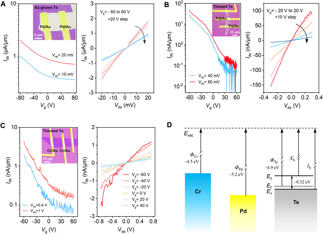
FIGURE 4. Characterizations of the pristine and thinned Te FETs. (A) Transfer and output curves of FET fabricated with as-grown Te nanosheet, and the inset shows the corresponding optical image of the device. (B) Transfer and output curves of FET fabricated with thinned Te. Inset shows the optical image of the device, and Pd/Au is employed as the source and drain electrodes. (C) Transfer and output curves of another thinned Te FET, in which Cr/Au is used as the electrode. (D) Schematic energy band profiles for Cr, Pd, and Te.
Optoelectronic characteristics of the Te FETs were further studied to demonstrate their applications in photodetectors. Schematic and optical images of the device are shown in Supplementary Figure S10. Figures 5A–C presents the Ids-Vds output curves (at Vg = −10 V) of Te phototransistors under the 980 nm, 1.55 μm, and 3.0 μm laser illumination with varying power densities, which demonstrate a broad response spectrum covering the entire SWIR wavelength (λ = 1–3 μm). The net photocurrent Iph increases monolithically with increasing incident power for all wavelengths. In contrast, the responsivity (R) decreases with increasing light intensity, which may be attributed to the decreased density of unoccupied states in Te and enhanced photocarrier recombination under high optical power (Supplementary Figure S11) (Xue et al., 2016; Zeng et al., 2018; Zeng et al., 2020; Wu D et al., 2021). Besides, the photoresponse could be further effectively modulated with electrostatic gating. Figures 5D–F presents the transfer characteristics of the Te transistor (upper part) and corresponding gate-dependent Iph (lower part) under different illumination wavelengths. Generally, the photocurrent and thus the R increase with negative gate voltage. For the 980 nm laser, the R reaches 2.2 AW−1 at an incident power density of 48 mWcm−2 at Vg of −80 V and Vds of 0.2 V. For the optical communication wavelength of 1.55 μm, a responsivity of 0.96 AW−1 is obtained under 64.4 mWcm−2 illumination density, together with an external quantum efficiency (EQE) of 76.5% and detectivity (D) of 2.2 × 10⁹ Jones (Figures 5G–I). The calculation details of these critical parameters (R, EQE, and D) are shown in Supplementary Figure S12 and Supplementary Note S1. Compared with 980 nm, the reduced photoresponse properties for 1.55 and 3.0 μm light are due to the lower absorption coefficient of Te for longer wavelengths (Amani et al., 2018; Tong et al., 2020).
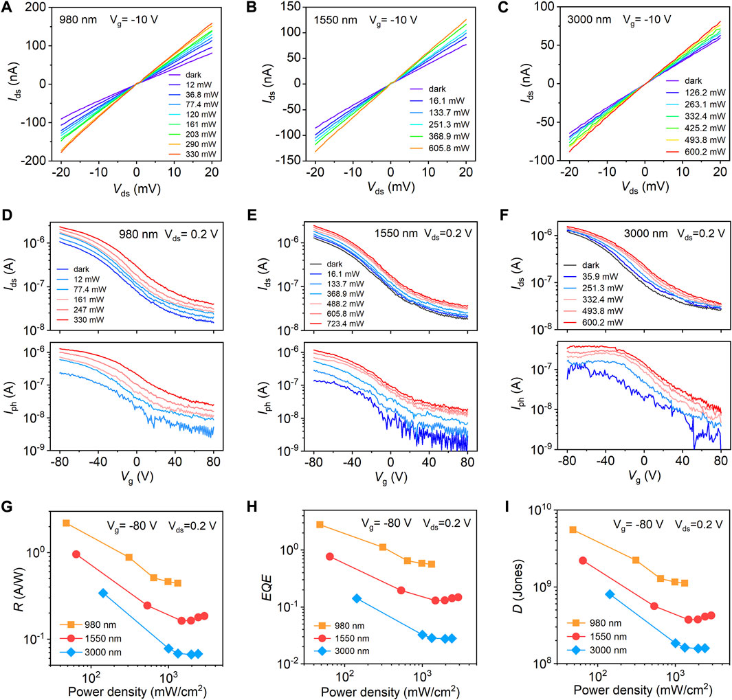
FIGURE 5. The Ids-Vds curves of Te phototransistors under varying 980 nm (A), 1,550 nm (B), and 3,000 nm (C) illumination power. The gate voltage Vg is fixed at -10 V. (D–F) Transfer characteristics (upper part) and gate-dependent net photocurrent Iph (lower part) under different illumination wavelengths. (G–I) Illumination power-dependent photoresponsivity (R), external quantum efficiency (EQE), and detectivity D for different wavelengths at Vg = −80 V and Vds = 0.2 V.
Polarized Raman characterization in Figures 1F–H has demonstrated the favorable optical anisotropy of Te, revealing its feasibility for polarized SWIR photodetection. In light of this, the polarization-resolved photoresponse of Te phototransistor under 1.55 μm illumination was further investigated, with the experimental setup schematically shown in Figure 6A. The linear polarization direction of the laser and incident optical power is fixed during measurement, and the Ids-Vds photoresponse curves are measured at different sample rotation angles. Figure 6B displays the contour map of polarized Iph-Vds characteristics of the Te transistor, exhibiting obvious periodic variation with the sample rotation angles and changes periodically. The polar plot of Iph as a function of sample rotation angle at Vds of 6 mV is shown in Figure 6C. The corresponding photocurrent Iph-Vds curves at each rotation angle are presented in Supplementary Figure S13. The anisotropic ratio, defined as the maximum Iph over the minimum, reaches up to ∼2.9, which is very competitive in the SWIR band and comparable with other widely-studied 2D materials such as BP and PdSe2 (Yuan et al., 2015; Pi et al., 2021). The results suggest that the 2D Te can be a promising material platform for future polarized infrared imaging applications.
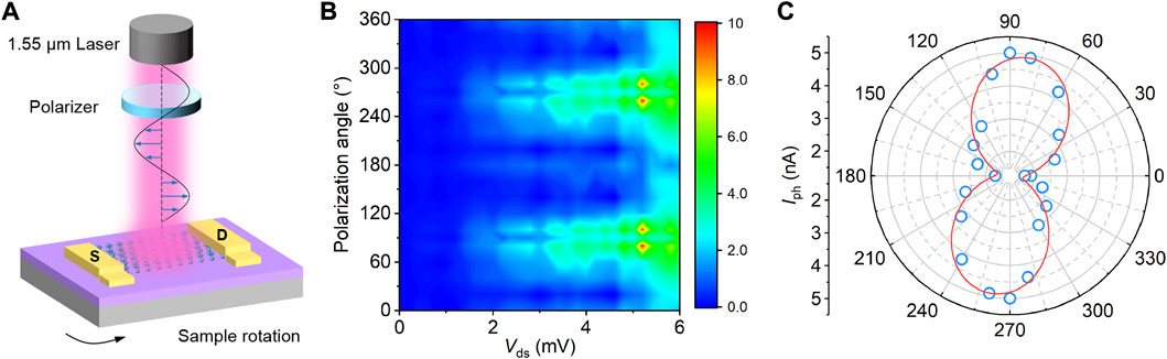
FIGURE 6. Polarized infrared photoresponse of the Te transistor under the incident wavelength of 1.55 μm. (A) Schematic experimental setup for measuring the polarization-resolved photoresponse. (B) Contour plot of polarized photoresponse characteristics of the Te phototransistor under constant 340 mW 1,550 nm illumination. (C) Polar plot of the Iph as a function of the sample rotation angle, the Vds is 6 mV.
In summary, we proposed a novel solution-processed strategy for the thickness engineering of 2D Te based on the oxidative-etching mechanism. The gradual material thickness reduction was readily achieved using appropriate oxidants, such as HNO2, H2O2, and KMnO4. Compared with the conventional physical thinning approaches, this method has several distinct advantages: Low cost, easy scalability, and facile processing conditions. In particular, site-specific thickness patterning was also realized in combination with the mature photolithography technique, which opens vast possibilities for arbitrarily tailoring the local properties of Te. The field-effect transistors fabricated with thinned Te present a significantly improved gate-tunability, thus promoting their applications in future logic devices. For optoelectronic applications, the response spectrum of Te phototransistors covers the whole SWIR band (λ = 1–3 μm). A favorable responsivity of 0.96 AW−1 and detectivity of 2.2 × 10⁹ Jones was obtained at the optical communication wavelength of 1.55 μm, together with an anisotropic photocurrent ratio of ∼2.9. As the thickness engineering approach is implemented by leveraging the material’s intrinsic chemical reactivity, it should apply to 2D Te prepared by other techniques, such as physical vapor deposition, chemical vapor deposition, or thermal deposition. Meanwhile, the feasibility of site-specific thinning may inspire the design of more sophisticated Te-based electronics and optoelectronics, which help realize its full device potential.
The original contributions presented in the study are included in the article/Supplementary Material, further inquiries can be directed to the corresponding authors.
PL and HY conceived the project and designed experiments. FC and LG performed the materials synthesis and processing. DC, CZ, and YY contributed to the device fabrication. FC performed the TEM characterization. FC, DC, and JL carried out XRD, Raman, AFM, and electrical characterizations under the supervision of DW. ZG and SM contributed to the data analysis.
This work is financially supported by Henan Provincial Key Science and Technology Research Projects (Grant No. 212102210131), and the Open Fund of the National Joint Engineering Research Center for Abrasion Control and Molding of Metal Materials (HKDNM2021012).
The authors declare that the research was conducted in the absence of any commercial or financial relationships that could be construed as a potential conflict of interest.
All claims expressed in this article are solely those of the authors and do not necessarily represent those of their affiliated organizations, or those of the publisher, the editors and the reviewers. Any product that may be evaluated in this article, or claim that may be made by its manufacturer, is not guaranteed or endorsed by the publisher.
The Supplementary Material for this article can be found online at: https://www.frontiersin.org/articles/10.3389/fchem.2022.1046010/full#supplementary-material
Agapito, L. A., Kioussis, N., Goddard, W. A., and Ong, N. P. (2013). Novel family of chiral-based topological insulators: elemental tellurium under strain. Phys. Rev. Lett. 110, 176401. doi:10.1103/PhysRevLett.110.176401
Amani, M., Tan, C., Zhang, G., Zhao, C., Bullock, J., Song, X., et al. (2018). Solution-synthesized high-mobility tellurium nanoflakes for short-wave infrared photodetectors. ACS Nano 12, 7253–7263. doi:10.1021/acsnano.8b03424
Bat-Erdene, M., Bati, A. S. R., Qin, J., Zhao, H., Zhong, Y. L., Shapter, J. G., et al. (2022). Elemental 2D materials: Solution-processed synthesis and applications in electrochemical ammonia production. Adv. Funct. Mat. 32, 2107280. doi:10.1002/adfm.202107280
Bockris, J. O. M., and Oldfield, L. F. (1955). The oxidation-reduction reactions of hydrogen peroxide at inert metal electrodes and mercury cathodes. Trans. Faraday Soc. 51, 249–259. doi:10.1039/TF9555100249
Castellanos-Gomez, A., Barkelid, M., Goossens, A. M., Calado, V. E., Van Der Zant, H. S. J., and Steele, G. A. (2012). Laser-thinning of MoS2: on demand generation of a single-layer semiconductor. Nano Lett. 12, 3187–3192. doi:10.1021/nl301164v
Chaves, A., Azadani, J. G., Alsalman, H., Da Costa, D. R., Frisenda, R., Chaves, A. J., et al. (2020). Bandgap engineering of two-dimensional semiconductor materials. npj 2D Mat. Appl. 4, 29. doi:10.1038/s41699-020-00162-4
Chen, J., Dai, Y., Ma, Y., Dai, X., Ho, W., and Xie, M. (2017). Ultrathin β-tellurium layers grown on highly oriented pyrolytic graphite by molecular-beam epitaxy. Nanoscale 9, 15945–15948. doi:10.1039/C7NR04085G
Deckoff-Jones, S., Wang, Y., Lin, H., Wu, W., and Hu, J. (2019). Tellurene: A multifunctional material for midinfrared optoelectronics. ACS Photonics 6, 1632–1638. doi:10.1021/acsphotonics.9b00694
Fan, F. R., Wang, R., Zhang, H., and Wu, W. (2021). Emerging beyond-graphene elemental 2D materials for energy and catalysis applications. Chem. Soc. Rev. 50, 10983–11031. doi:10.1039/C9CS00821G
Glavin, N. R., Rao, R., Varshney, V., Bianco, E., Apte, A., Roy, A., et al. (2020). Emerging applications of elemental 2D materials. Adv. Mat. 32, 1904302. doi:10.1002/adma.201904302
He, Z., Yang, Y., Liang, H.-W., Liu, J.-W., and Yu, S.-H. (2019). Nanowire genome: A magic toolbox for 1D nanostructures. Adv. Mat. 31, 1902807. doi:10.1002/adma.201902807
Hu, H., Zeng, Y., Gao, S., Wang, R., Zhao, J., You, K., et al. (2021). Fast solution method to prepare hexagonal tellurium nanosheets for optoelectronic and ultrafast photonic applications. J. Mat. Chem. C 9, 508–516. doi:10.1039/D0TC04106H
Huang, X., Guan, J., Lin, Z., Liu, B., Xing, S., Wang, W., et al. (2017). Epitaxial growth and band structure of Te film on graphene. Nano Lett. 17, 4619–4623. doi:10.1021/acs.nanolett.7b01029
Huang, B., Lei, Z., Cao, X., Wei, A., Tao, L., Yang, Y., et al. (2021). High-quality two-dimensional tellurium flakes grown by high-temperature vapor deposition. J. Mat. Chem. C 9, 14394–14400. doi:10.1039/D1TC02936C
Li, C., Zhang, L., Gong, T., Cheng, Y., Li, L., Li, L., et al. (2021). Study of the growth mechanism of solution-synthesized symmetric tellurium nanoflakes at atomic resolution. Small 17, 2005801. doi:10.1002/smll.202005801
Lin, Z., Wang, C., and Chai, Y. (2020). Emerging group-VI elemental 2D materials: Preparations, properties, and device applications. Small 16, 2003319. doi:10.1002/smll.202003319
Londoño-Calderon, A., Williams, D. J., Ophus, C., and Pettes, M. T. (2020). 1D to 2D transition in tellurium observed by 4D electron microscopy. Small 16, 2005447. doi:10.1002/smll.202005447
Ma, W., Gao, Y., Shang, L., Zhou, W., Yao, N., Jiang, L., et al. (2022). Ultrabroadband tellurium photoelectric detector from visible to millimeter wave. Adv. Sci. (Weinh). 9, 2103873. doi:10.1002/advs.202103873
Mannix, A. J., Kiraly, B., Hersam, M. C., and Guisinger, N. P. (2017). Synthesis and Chemistry of elemental 2D materials. Nat. Rev. Chem. 1, 0014. doi:10.1038/s41570-016-0014
Nan, H., Zhou, R., Gu, X., Xiao, S., and Ostrikov, K. (2019). Recent advances in plasma modification of 2D transition metal dichalcogenides. Nanoscale 11, 19202–19213. doi:10.1039/C9NR05522C
Nevalaita, J., and Koskinen, P. (2018). Atlas for the properties of elemental two-dimensional metals. Phys. Rev. B 97, 035411. doi:10.1103/PhysRevB.97.035411
Peng, M., Xie, R., Wang, Z., Wang, P., Wang, F., Ge, H., et al. (2021). Blackbody-sensitive room-temperature infrared photodetectors based on low-dimensional tellurium grown by chemical vapor deposition. Sci. Adv. 7, eabf7358. doi:10.1126/sciadv.abf7358
Pi, L., Hu, C., Shen, W., Li, L., Luo, P., Hu, X., et al. (2021). Highly in-plane anisotropic 2D PdSe2 for polarized photodetection with orientation selectivity. Adv. Funct. Mat. 31, 2006774. doi:10.1002/adfm.202006774
Pine, A. S., and Dresselhaus, G. (1971). Raman spectra and lattice dynamics of tellurium. Phys. Rev. B 4, 356–371. doi:10.1103/PhysRevB.4.356
Qiao, J., Pan, Y., Yang, F., Wang, C., Chai, Y., and Ji, W. (2018). Few-layer tellurium: One-Dimensional-Like layered elementary semiconductor with striking physical properties. Sci. Bull. (Beijing). 63, 159–168. doi:10.1016/j.scib.2018.01.010
Si, J., Yu, J., Shen, Y., Zeng, M., and Fu, L. (2021). Elemental 2D materials: Progress and perspectives toward unconventional structures. Small Struct. 2, 2000101. doi:10.1002/sstr.202000101
Tao, L., Han, L., Yue, Q., Yao, B., Yang, Y., and Huo, N. (2021). High hole mobility in physical vapour deposition-grown tellurium-based transistors. R. Soc. Open Sci. 8, 210554. doi:10.1098/rsos.210554
Tong, L., Huang, X., Wang, P., Ye, L., Peng, M., An, L., et al. (2020). Stable mid-infrared polarization imaging based on quasi-2D tellurium at room temperature. Nat. Commun. 11, 2308. doi:10.1038/s41467-020-16125-8
Wakafuji, Y., Moriya, R., Masubuchi, S., Watanabe, K., Taniguchi, T., and Machida, T. (2020). 3D manipulation of 2D materials using microdome polymer. Nano Lett. 20, 2486–2492. doi:10.1021/acs.nanolett.9b05228
Wang, Q., Safdar, M., Xu, K., Mirza, M., Wang, Z., and He, J. (2014). Van der Waals epitaxy and photoresponse of hexagonal tellurium nanoplates on flexible mica sheets. ACS Nano 8, 7497–7505. doi:10.1021/nn5028104
Wang, D., Wang, Y., Chen, X., Zhu, Y., Zhan, K., Cheng, H., et al. (2016). Layer-by-Layer thinning of two-dimensional MoS2 films by using a focused ion beam. Nanoscale 8, 4107–4112. doi:10.1039/C5NR05768J
Wang, Y., Qiu, G., Wang, R., Huang, S., Wang, Q., Liu, Y., et al. (2018). Field-effect transistors made from solution-grown two-dimensional tellurene. Nat. Electron. 1, 228–236. doi:10.1038/s41928-018-0058-4
Wang, Y., De Souza Borges Ferreira, R., Wang, R., Qiu, G., Li, G., Qin, Y., et al. (2019). Data-driven and probabilistic learning of the process-structure-property relationship in solution-grown tellurene for optimized nanomanufacturing of high-performance nanoelectronics. Nano Energy 57, 480–491. doi:10.1016/j.nanoen.2018.12.065
Wang, C., Wang, P., Chen, S., Wen, W., Xiong, W., Liu, Z., et al. (2022). Anisotropic properties of tellurium nanoflakes probed by polarized Raman and transient absorption microscopy: Implications for polarization-sensitive applications. ACS Appl. Nano Mat. 5, 1767–1774. doi:10.1021/acsanm.1c03132
Weidmann, E. J., and Anderson, J. C. (1971). Structure and growth of oriented tellurium thin films. Thin Solid Films 7, 265–276. doi:10.1016/0040-6090(71)90073-3
Wu, D., Guo, J., Wang, C., Ren, X., Chen, Y., Lin, P., et al. (2021). Ultrabroadband and high-detectivity photodetector based on WS2/Ge heterojunction through defect engineering and interface passivation. ACS Nano 15, 10119–10129. doi:10.1021/acsnano.1c02007
Wu, Z., Qi, J., Wang, W., Zeng, Z., and He, Q. (2021). Emerging elemental two-dimensional materials for energy applications. J. Mat. Chem. A 9, 18793–18817. doi:10.1039/D1TA03676A
Xu, L., Liang, H.-W., Li, H.-H., Wang, K., Yang, Y., Song, L.-T., et al. (2015). Understanding the stability and reactivity of ultrathin tellurium nanowires in solution: an emerging platform for chemical transformation and material design. Nano Res. 8, 1081–1097. doi:10.1007/s12274-014-0586-9
Xue, Y., Zhang, Y., Liu, Y., Liu, H., Song, J., Sophia, J., et al. (2016). Scalable production of a few-layer MoS2/WS2 vertical heterojunction array and its application for photodetectors. ACS Nano 10, 573–580. doi:10.1021/acsnano.5b05596
Yang, Y., Wang, K., Liang, H.-W., Liu, G.-Q., Feng, M., Xu, L., et al. (2015). A new generation of alloyed/multimetal chalcogenide nanowires by chemical transformation. Sci. Adv. 1, e1500714. doi:10.1126/sciadv.1500714
Yang, Y., Liu, G.-Q., Gao, M.-R., Xia, Y., and Yu, S.-H. (2018). Selective oxidation mediated synthesis of unique SexTey nanotubes, their assembled thin films and photoconductivity. Nano Res. 11, 665–675. doi:10.1007/s12274-017-1673-5
Yang, P., Zha, J., Gao, G., Zheng, L., Huang, H., Xia, Y., et al. (2022). Growth of tellurium nanobelts on h-BN for P-type transistors with ultrahigh hole mobility. Nano-Micro Lett. 14, 109. doi:10.1007/s40820-022-00852-2
Yao, J., Chen, F., Li, J., Du, J., Wu, D., Tian, Y., et al. (2021a). Mixed-dimensional Te/CdS van der Waals heterojunction for self-powered broadband photodetector. Nanotechnology 32, 415201. doi:10.1088/1361-6528/ac10e6
Yao, J., Chen, F., Li, J., Du, J., Wu, D., Tian, Y., et al. (2021b). A high-performance short-wave infrared phototransistor based on a 2D tellurium/MoS2 van der Waals heterojunction. J. Mat. Chem. C 9, 13123–13131. doi:10.1039/D1TC02502C
Yuan, H., Liu, X., Afshinmanesh, F., Li, W., Xu, G., Sun, J., et al. (2015). Polarization-sensitive broadband photodetector using a black phosphorus vertical p-n junction. Nat. Nanotechnol. 10, 707–713. doi:10.1038/nnano.2015.112
Zeng, L.-H., Lin, S.-H., Li, Z.-J., Zhang, Z.-X., Zhang, T.-F., Xie, C., et al. (2018). Fast, self-driven, air-stable, and broadband photodetector based on vertically aligned PtSe2/GaAs heterojunction. Adv. Funct. Mat. 28, 1705970. doi:10.1002/adfm.201705970
Zeng, L., Wu, D., Jie, J., Ren, X., Hu, X., Lau, S. P., et al. (2020). Van der Waals epitaxial growth of mosaic-like 2D platinum ditelluride layers for room-temperature mid-infrared photodetection up to 10.6 µm. Adv. Mat. 32, 2004412. doi:10.1002/adma.202004412
Zhang, X., Yu, H., Tang, W., Wei, X., Gao, L., Hong, M., et al. (2022). All-van-der-Waals barrier-free contacts for high-mobility transistors. Adv. Mat. 34, 2109521. doi:10.1002/adma.202109521
Zhao, C., Tan, C., Lien, D.-H., Song, X., Amani, M., Hettick, M., et al. (2020). Evaporated tellurium thin films for P-type field-effect transistors and circuits. Nat. Nanotechnol. 15, 53–58. doi:10.1038/s41565-019-0585-9
Zhao, Q., Gao, F., Chen, H., Gao, W., Xia, M., Pan, Y., et al. (2021). High performance polarization-sensitive self-powered imaging photodetectors based on a p-Te/n-MoSe2 van der Waals heterojunction with strong interlayer transition. Mat. Horiz. 8, 3113–3123. doi:10.1039/D1MH01287H
Zhao, X., Shi, J., Yin, Q., Dong, Z., Zhang, Y., Kang, L., et al. (2022). Controllable synthesis of high-quality two-dimensional tellurium by a facile chemical vapor transport strategy. iScience 25, 103594. doi:10.1016/j.isci.2021.103594
Zheng, B., Wu, Z., Guo, F., Ding, R., Mao, J., Xie, M., et al. (2021). Large-area tellurium/germanium heterojunction grown by molecular beam epitaxy for high-performance self-powered photodetector. Adv. Opt. Mat. 9, 2101052. doi:10.1002/adom.202101052
Zheng, W., Li, Y., Liu, M., and Lee, L. Y. S. (2021). Few-Layer tellurium: Cathodic exfoliation and doping for collaborative hydrogen evolution. Small 17, 2007768. doi:10.1002/smll.202007768
Zhou, D., Li, H., Si, N., Li, H., Fuchs, H., and Niu, T. (2021). Epitaxial growth of main group monoelemental 2D materials. Adv. Funct. Mat. 31, 2006997. doi:10.1002/adfm.202006997
Keywords: tellurene, oxidative etching, thickness engineering, field-effect transistors, polarizd infrared photodetection
Citation: Chen F, Cao D, Li J, Yan Y, Wu D, Zhang C, Gao L, Guo Z, Ma S, Yu H and Lin P (2022) Solution-processed thickness engineering of tellurene for field-effect transistors and polarized infrared photodetectors. Front. Chem. 10:1046010. doi: 10.3389/fchem.2022.1046010
Received: 16 September 2022; Accepted: 04 October 2022;
Published: 13 October 2022.
Edited by:
Xiang Chen, Nanjing University of Science and Technology, ChinaReviewed by:
Longhui Zeng, Hong Kong Polytechnic University, Hong Kong, SAR ChinaCopyright © 2022 Chen, Cao, Li, Yan, Wu, Zhang, Gao, Guo, Ma, Yu and Lin. This is an open-access article distributed under the terms of the Creative Commons Attribution License (CC BY). The use, distribution or reproduction in other forums is permitted, provided the original author(s) and the copyright owner(s) are credited and that the original publication in this journal is cited, in accordance with accepted academic practice. No use, distribution or reproduction is permitted which does not comply with these terms.
*Correspondence: Huihui Yu, eXVodWlodWlAdXN0Yi5lZHUuY24=; Pei Lin, bGlucGVpQHp6dS5lZHUuY24=
†These authors have contributed equally to this work and share first authorship
Disclaimer: All claims expressed in this article are solely those of the authors and do not necessarily represent those of their affiliated organizations, or those of the publisher, the editors and the reviewers. Any product that may be evaluated in this article or claim that may be made by its manufacturer is not guaranteed or endorsed by the publisher.
Research integrity at Frontiers
Learn more about the work of our research integrity team to safeguard the quality of each article we publish.