 Ke Yang
 Tianyu Liu1*
 Xiao-Dong Zhang
95% of researchers rate our articles as excellent or good
Learn more about the work of our research integrity team to safeguard the quality of each article we publish.
Find out more
ORIGINAL RESEARCH article
Front. Chem. , 18 June 2021
Sec. Nanoscience
Volume 9 - 2021 | https://doi.org/10.3389/fchem.2021.700250
This article is part of the Research Topic NIR-II Fluorophore and Imaging View all 11 articles
The fluorescence-based optical imaging in the second near-infrared region (NIR-II, 1,000–1,700 nm) has broad applications in the biomedical field, but it is still difficult to find new NIR-II fluorescence materials in the two dimension. As a crucial characteristic of the electronic structure, the band structure determines the fundamental properties of two-dimensional materials, such as their optical excitations and electronic transportation. Therefore, we calculated the electronic structures and optical properties of different crystalline phases (1T phase and 2H phase) of pure monolayer MoS2 films and found that the 1T phase has better absorption and thus better fluorescence in the NIR-II window. However, its poor stability makes the 1T-phase MoS2 less useful in vivo bioimaging. By introducing vacancy defects and doping with foreign atoms, we successfully tuned the bandgap of the monolayer 2H-MoS2 and activated it in the NIR-II. Our results show that by engineering the vacancy defects, the bandgap of the 2H phase can be tailored to around 1 eV, and there are three candidates of vacancy structures that exhibit strong absorption in the NIR-II.
The NIR-II fluorescence probe has attracted much attention in recent years. Compared with the visible light (400–700 nm) and the NIR-I (700–900 nm) imaging, the NIR-II (1,000–1,700 nm) imaging has longer fluorescence wavelength and stronger penetrating ability, which has shown great potential in tumor diagnosis and in vivo in situ imaging. Since Dai et al. discovered that carbon nanotubes (Jiao et al., 2009; Welsher et al., 2009), fluorescent quantum dots (Hong et al., 2012), small molecules (Antaris et al., 2016), and rare earth metals have good fluorescence and biocompatibility in the NIR-II window (Sun et al., 2019), the development of this technology has been widely promoted (Hong et al., 2012; Fan et al., 2018). With the rapid development of imaging equipment and technology in the NIR-II (Zhang et al., 2016; Liu et al., 2019), finding new fluorescence material in the NIR-II is still a pressing task, which requires us to find semiconductor materials with a bandgap less than 1.0 eV. It is well-known that two-dimensional materials have obvious advantages in bandgap modulation; however, in recent years, there have been very few theoretical works studying the fluorescence materials in the NIR-II. As a result, searching for the well-behaved two-dimensional materials relies more on perceptions and arduous experiments. Among these efforts, layered transition metal dichalcogenides (TMDs) (Soares et al., 2020) have been widely studied in recent years due to their unique atomic structure, band structure, and optical properties (Wang et al., 2012). Thereinto, MoS2 with natural bandgap (1.2∼1.8 eV) come to the fore. In the benefit of that, all the TMDs2-MX2 (M = Mo, W; X = S, Se) possess similar electronic structures and thus similar properties in photoelectric and catalytic processes; MoS2 is usually studied as a representative for TMDs (Hong et al., 2017).
MoS2 has three types of crystal structures: 1T (trigonal), 2H (hexagonal), and 3R (rhombohedral). The 1T phase is metallic, while the 2H and the 3R are semiconductors. Besides, the 2H phase is the most stable one (Xu et al., 2016). 1T and 3R are metastable and can be converted back to the 2H phase (Chaste et al., 2020) under the conditions of heating and annealing (Geng et al., 2016; Byrley et al., 2019). As shown in Figure 1, a monolayer MoS2 film is composed of two layers of sulfur atoms sandwiched by one layer of Mo atoms (Helveg et al., 2000). The atoms of different layers are bonded by strong covalent bonds. The thickness of the monolayer MoS2 is about 6.5 Å. The upper and lower S atoms of the 2H phase overlap completely in the direction perpendicular to the film, while the upper and lower S atoms of the 1T phase do not overlap at all.
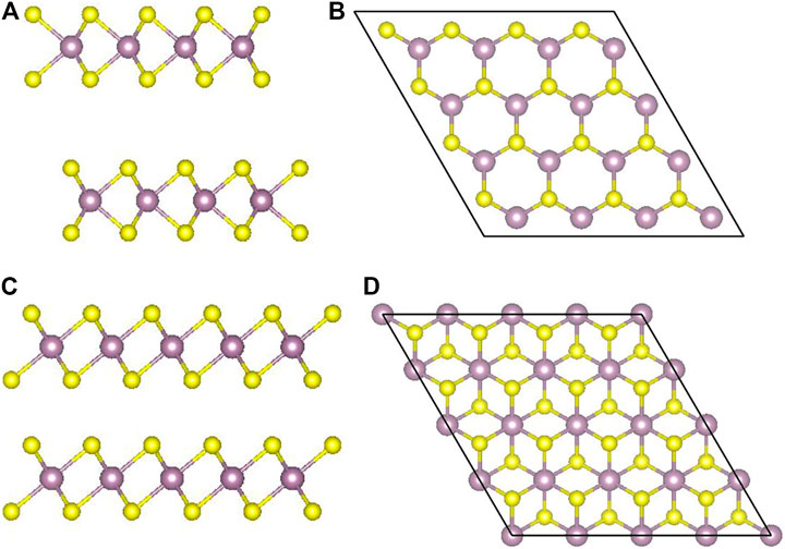
FIGURE 1. 1T- and 2H-phase MoS2: (A) and (B) the layered structure of 2H-MoS2 and the top view in z direction; (C) and (D) the same for 1T-MoS2.
The layered nature of bulk MoS2 makes it easy to slide subjected to external friction (Zhang et al., 2009). Therefore, 2H-MoS2 has been widely used in the field of lubricants (Lahouij et al., 2012) and hydrodesulfurization catalysts (Gutiérrez et al., 2014). When reducing to single-layer structures, the bandgap of MoS2 increases from ∼1.2 to ∼1.8 eV and changes from indirect bandgap to direct, which indicates that the layered MoS2 bandgap is adjustable and has potential applications in optoelectronics (Steinhoff et al., 2015). Because of a direct bandgap of ∼1.8 eV, monolayer MoS2 has great applications in photodetectors and plasma devices. Moreover, as an attractive nanomaterial for photothermal cancer therapy, 1T-phase MoS2 is a highly effective reagent in photoacoustic imaging (PAI)–guided photothermal therapy (PTT) in the NIR-II window (Zhou et al., 2020). Under 1,064 nm laser irradiation, it can effectively ablate cancer cells in vitro and tumors in vivo. However, monolayer 1T-MoS2 is less stable than the 1H phase. Therefore, it is necessary to find a way to engineer 1H-MoS2, so that it can be used for fluorescence in the NIR-II. At present, different point defects and antisite defects (Nakayasu et al., 2019) have been observed experimentally. In the study of Zhou et al., point vacancies are more common than antisite defects, which is consistent with their DFT calculations, and mono-vacancy VS (only one S atom missing from the sulfur sublattice site) has the lowest formation energy. And VMoS2 (containing a VMo and VS2 pair), VMoS3 (vacancy complex of Mo atom and nearby three S atoms), and VMoS6 (vacancy complex of Mo atom nearby three S pairs) have relatively poor structural stability due to its higher formation energy (Zhou et al., 2013). Mann et al. studied MoS2(1-x) Se2x doped with different concentrations of Se and concluded that the bandgap decreases linearly with increasing Se-doping concentration with the tuning window ranging from 1.85 eV (pure MoS2) to 1.55 eV (pure MoSe2) (Li et al., 2014), which provides a feasible way to manipulate of the bandgap of MoS2 (Mann et al., 2014). Dumcenco et al. reported single-layer Mo1-xWxS2 semiconductor alloy with a bandgap ranging from 1.82 eV to 1.99 eV, not significantly depending on the concentration of W (Dumcenco et al., 2013). Inspired by previous studies (Zeng et al., 2020), we calculated the electronic structures and optical properties of 1T and 2H phases of monolayer MoS2 films by the first-principle method. By adjusting the position of the vacancy defects and dopings, we predict three possible structures that can be applied in the NIR-II, which provides a potential direction for experimentally studying NIR-II fluorescence of single-layer MoS2 films.
The article is organized as below. Theories reviews basic steps in calculating the optical properties from the first-principal methods. Results and Discussion presents our results and discussions on band structures, ground-state energies, and absorption spectra for different defects and dopings. The technique details are listed in Methods.
In this section, we will discuss the basic concepts of how to get the absorption spectra of two-dimension materials from the first-principle calculations. Although one can get the plasma frequency and the dynamic dielectric function from VASP directly and the absorption spectra seem to be obtained straightforwardly from the imaginary part of the dielectric function, special attention should be paid to the metallic phase. According to the band structure as shown in Figure 2B, 1T-phase monolayer MoS2 behaves like a metal. Therefore, its dynamic dielectric function consists of two parts: one from the interband transition, which can be obtained from the optical calculation module in VASP, the other from the intraband transition, which requires some extra steps recapitulated as below.
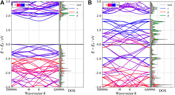
FIGURE 2. Band structures and pDOS of 2H-MoS2(A) and 1T-MoS2(B). The blue (red) curves are mainly contributed by atom Mo (S) in the band structure. The shadow area in the pDOS refers to the total DOS, and the solid lines of different colors refer to the projection on different orbitals indicated by the legend inside the figure.
For metals, the optical complex dielectric function consists of interband and Drude-like intraband contributions (Guan et al., 2015):
The imaginary part of the interband dielectric function is given by the first-principle calculations as follows (Gajdoš et al., 2006)
where
where
where
In this study, we took into account the electron–electron scattering only (
where
Different from bulk materials, the absorbance of two-dimensional materials is defined by (Wang et al., 2019):
The in-plane 2D optical conductivity is directly related to the corresponding
Combining with the above equation, we obtained the absorption spectra
In this subsection, we will compare the band structures and the optical properties of monolayers 1T-MoS2 and 2H-MoS2 without defects and doping. The band structures and density of states (DOS) of 1T and 2H phases are shown in Figure 2. It shows that monolayer 2H-MoS2 remains a semiconductor as the bulk MoS2, while monolayer 1T-MoS2 turns into a metal, whose states near the Fermi surface mainly come from the Mo–d orbit and the S–p orbit. The 2H-phase monolayer shows a direct bandgap of 1.65 eV, close to the calculated result of Kan et al. (1.67 eV) and Johari et al. (1.68 eV) (Johari and Shenoy, 2012; Kan et al., 2014). The results are in the same bandgap as GGA-PBE predicts (Komsa and Krasheninnikov, 2015), and this ensures the rationality of the calculated parameters in this study. However, since the DFT-GGA tends to underestimate the bandgap, our result is lower than the experimental value ∼1.8 eV (Kam and Parkinson, 1982; Mak et al., 2010).
The optical properties of the two phases are shown in Figure 3. 2H-MoS2 shows peaks at 1.89 eV and 2.82 eV in the imaginary part of the complex dielectric functions (Figure 3A), which is mainly due to the electron transition between the highest valence band Mo–3d orbit and the conduction bands Mo–3d and S–p orbitals, according to the partial density of states (pDOS) as shown in Figure 2. The monolayer 2H-MoS2 imaginary part of the dielectric functions peaks at 1.89 eV and matches the lower absorption resonance in both its position and width. Therefore, we attribute the photoluminescence of monolayer MoS2 to direct-gap luminescence. These findings are in good agreement with the experimental results of Mak et al. (Mak et al., 2010) and previous calculations (Zeng et al., 2020) for monolayer MoS2 (Kumar and Ahluwalia, 2012). The transition of the 1T phase occurs at a lower energy of 1.12 eV, corresponding to the Mo–d and S–p transitions. The characteristic peaks in the dielectric functions for each phase lead to the distinct absorption spectra in Figure 3B. The 2H phase mainly absorbs light with a wavelength below 700 nm, while the 1T phase shows a strong absorption in the NIR-II window and an absorption peak at 1050 nm, which is consistent with the experimental conclusion of Zhou et al. (Zhou et al., 2020). However, the 1T phase is less stable than the 2H phase. Therefore, it will be useful to find a way to modify the band structure of the 2H phase while keeping its stability. We found that the introduction of vacancy defects or doping of foreign atoms into the 2H phase shows great promise for its application in the NIR-II window. The results will be presented in rest of the article.
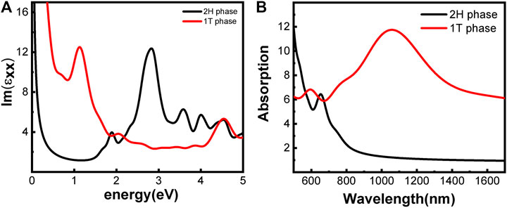
FIGURE 3. Optical properties of monolayer MoS2 without defect and doping: (A) imaginary part of the dielectric function; (B) absorption spectra. The phases are indicated by color.
Point defects in monolayer MoS2 are attractive because defects play a crucial role in manipulating its electrical and optical properties. Therefore, we designed the supercell of 2H-MoS2 with different numbers of S-vacancy, whose configurations have been plotted in Figure 4. Figure 4A shows single S-vacancy structure, and Figures 4C,D,F show two S-vacancies in the same atomic plane. Figures 4B,G,H show two S-vacancy structures in different atomic planes. Figure 4E compares the ground-state energy of the six configurations of double S-vacancies, demonstrating the structure stability, indicating that configurations V-S2-1, V-S2-2, and V-S2-6 are relatively stable, compared to V-S2-3, V-S2-4, and V-S2-5. Figure 4J shows triple S-vacancy structures in the same plane. Figures 4K,L show the triple S-vacancy structures in different planes. Figure 4I compares the ground-state energy of the three configurations of triple S-vacancies and indicates configuration V-S3-2 is the most stable among the three, while V-S3-1 is the worst. To explore the influence of S-vacancy on the electronic structure of the system, we calculated the band and pDOS, as shown in Figure 5, and found that different S-vacancy defects induce different energy levels contributed by Mo–d and S–p in the bandgap relative to the pure MoS2, which are distributed around 1 eV above the Fermi energy. In addition, it is noted that the density of states of the defect states in the bandgap increases with the increasing number of vacancies. The introduction of vacancies significantly reduces the bandgap. We also summarized the width of bandgap and the number of vacancies in Table 1 but found there is no direct relation between the two.
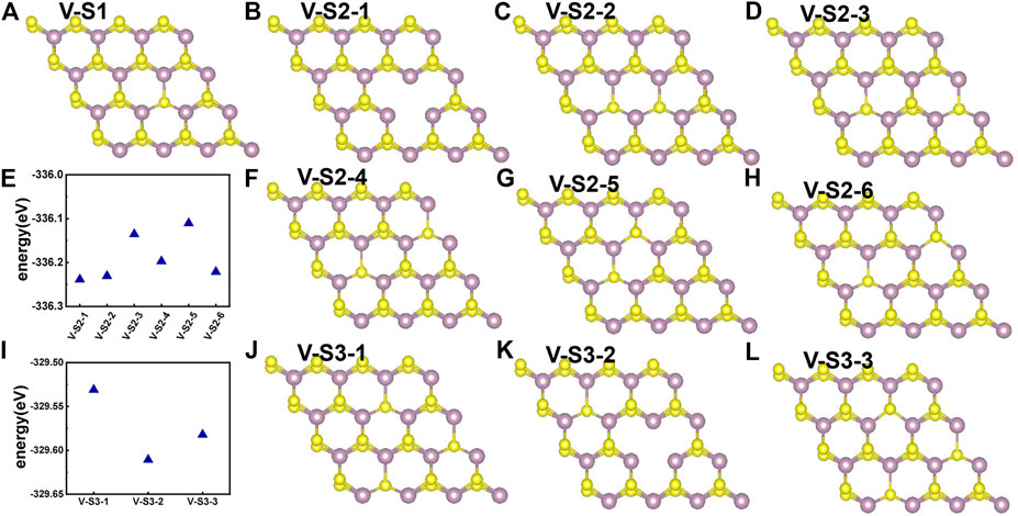
FIGURE 4. Different S-vacancy defect structures of 2H-MoS2, rotated by an angle to distinguish the two S layers: (A) single S-vacancy; (B–D) and (F–H) six types of configuration for double S-vacancies; (J–L) three types of configuration for triple S-vacancies; (E) and (I) compares the ground-state energy of double and triple S-vacancies.
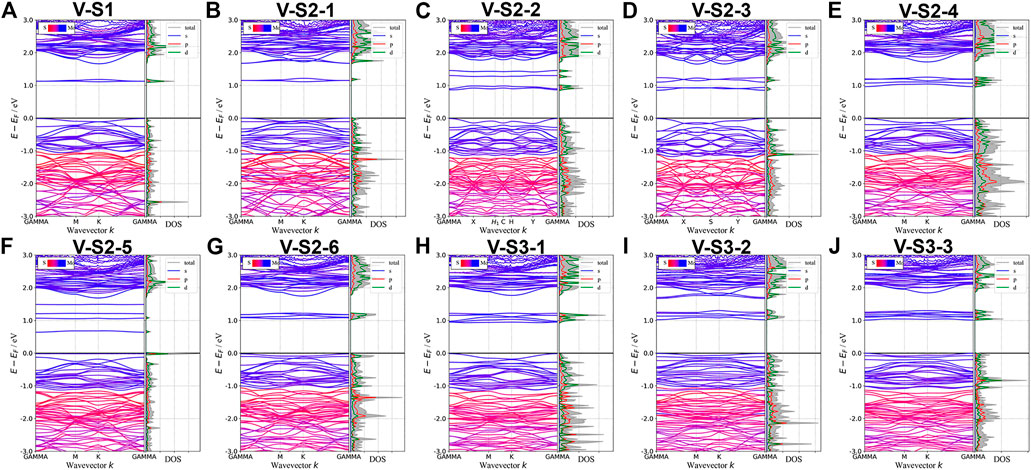
FIGURE 5. Band structures and pDOS of monolayer 2H-MoS2 with different S-vacancy defects. The labels of different vacancy structures are denoted above each figure. The corresponding atomic configurations can be referred to Figure 4.
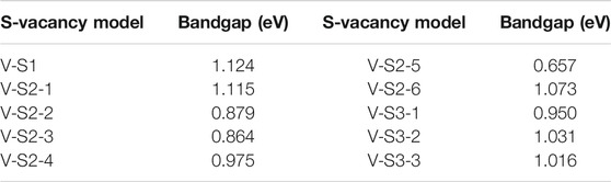
TABLE 1. Bandgap of different S-vacancy model.
Next, we studied the effects of S-vacancies on the optical properties. The imaginary part of the dielectric function is highly related to the absorption coefficient of the material. As shown in Figure 6A, in the presence of S-vacancy, the imaginary part of the dielectric function appears at a transition peak around 1 eV due to the energy levels between the bandgap of pure MoS2 (Figure 5), but the transition peak around 1 eV is lower than the peak at the higher energy. Rai et al. studied the optical properties of the S-vacancy concentration from 0 to 50% (0, 12.5, 25, 37.5, and 50%) and found a transition peak at a lower energy range, which would significantly increase with the increasing vacancy concentration (Rai et al., 2020). However, our calculations show that as the number of vacancies increases, the stability of the structure becomes worse. Although the density of defect states is small, it enhances the absorption in the NIR-II window significantly, as shown in Figure 6B. Taken together, the stability of the ground-state energy and absorbance, configurations V-S2-2, V-S2-3, and V-S2-6 are the best whose peaks are at 1,150 nm, 1,240 nm, and 980 nm, respectively.
FIGURE 6. Optical properties of monolayer 2H-MoS2 with different S-vacancy defects: (A) the imaginary part of the dynamic dielectric function; (B) absorption spectra. The black dotted line is for pure monolayer 2H-MoS2. The labels in the legend refer to different vacancy structures as shown in Figure 4.
Figures 7A–D,F give the different Mo-vacancy structures. In analogy to the S-vacancy structures, we considered the configurations of single, double, and triple Mo-vacancies. Judging from the ground-state energy, as shown in Figure 7E, V-Mo2-2 is the most stable among the configurations of double Mo-vacancies. With introducing Mo-vacancy, monolayer 2H-MoS2 tends to be a metal; as shown in Figure 8, except for the configurations of V-Mo1 and V-Mo2-2 whose bandgaps are 0.26 eV and 0.04 eV, respectively. The occupied states at the Fermi level are mainly contributed by the S–p and Mo–d orbitals. Figure 9 shows the dynamic dielectric function and the absorption spectra of the series of configurations of Mo-vacancy. It can be seen from the imaginary part of the dielectric function that the peak at 2.81 eV is quenching with the increasing number of Mo-vacancy, which is consistent with the band structure analysis in previous sections. In the first-principle calculations of Feng et al. (Feng et al., 2018), for monolayer MoS2 with lower Mo-vacancy concentration (4%), the imaginary part of the complex dielectric function has a slight blue shift, while for monolayer MoS2 with higher Mo-vacancy concentration (6.25 and 11%), the imaginary part of the complex dielectric function has a significant red shift. Our calculation results are consistent with the conclusion of Feng et al. that when Mo-vacancy concentration is high (6.26, 12.5, and 18.75%), the imaginary part of complex dielectric function of defective monolayer MoS2 appears obvious red shift. At low energy, V-Mo1 and V-Mo2-1 have an obvious transition peak at 0.93 eV, and V-Mo3 has a small transition peak at 1.56 eV. The red shift explains the dramatical improvement of the absorption in the NIR-II window, as shown in Figure 9B, where both V-Mo1 and V-Mo2-1 have an absorption peak at 1,270 nm. Considering the structure instability of V-Mo2-1 compared with the other two configurations of double Mo-vacancies, V-Mo1 may be a better choice for NIR-II applications.
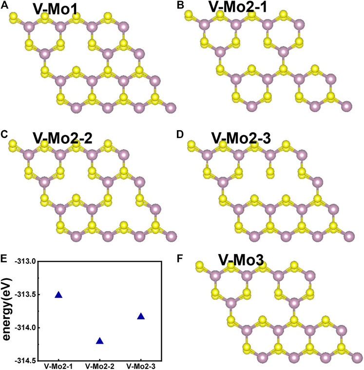
FIGURE 7. Different Mo-vacancy defect structures of 2H-MoS2, rotated by an angle to distinguish the two S layers: (A) single Mo-vacancy; (B–D) three configurations of double Mo-vacancies; (F) one configuration of triple Mo-vacancies; (E) comparison of the ground-state energies of different configurations of double Mo-vacancies.
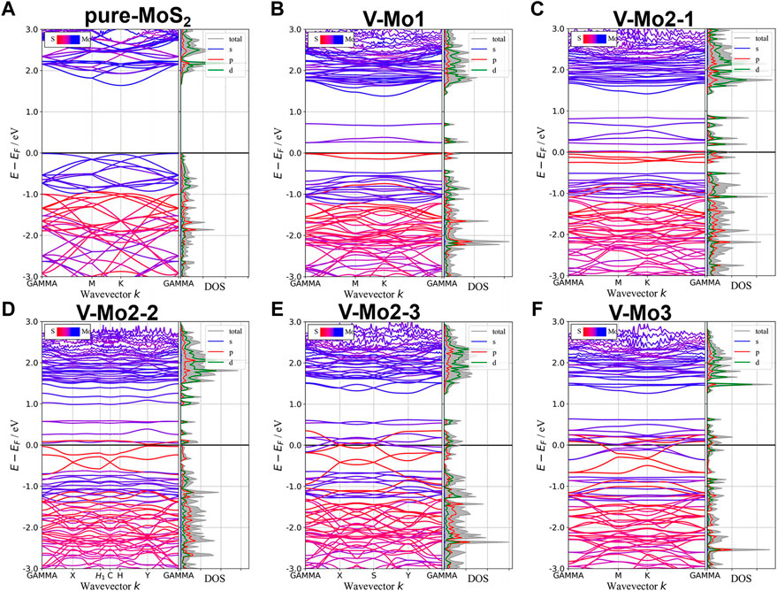
FIGURE 8. Band structures and pDOS of monolayer 2H-MoS2 with different Mo-vacancy defects. The labels of different vacancy structures are denoted above each figure. The corresponding atomic configurations can be referred to Figure 7.
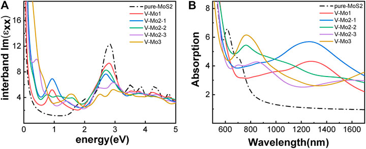
FIGURE 9. Optical properties of monolayer 2H-MoS2 with different Mo-vacancy defects: (A) the imaginary part of the dynamic dielectric function; (B) absorption spectra. The black dotted line is for pure monolayer 2H-MoS2. The labels in the legend refer to different vacancy structures, as shown in Figure 7.
Besides introducing vacancies, foreign atom doping is also a common method to manipulate the bandgap. As shown in Figure 10, we studied the substitution of atom S with C, Si, and Se and atom Mo with designed structures in which different elements replaced single S atom or single Mo atom with Ag, Au, Cr, Pd, Ru, and Sb. C, Si, and Se to replace S, respectively, and Ag, Au, Cr, Pd, Ru, and Sb to replace Mo, respectively. For dopants that fill single S-vacancy, C and Si have energy levels in the middle of the gap, while Se does not produce any localized states, as Komsa et al. expected in their work (Komsa et al., 2012). As shown in Figure 11, the doping of C and Si produces energy levels at 0.99 eV and 0.86 eV above the Fermi energy, respectively, and the doping of Se makes the bandgap increase to 1.73 eV, and our calculation result is in accordance with their findings. The doping of Ag, Au, Ru, and Sb turns the monolayer 2H-MoS2 into a metal. The doping of Cr and Ru leads to an impurity level within the original bandgap reduces the bandgap to 1.48 eV and 0.32 eV, respectively, which is consistent with those of Komsa et al., who observed vacancies filling and discussed the prospects for electron beam–mediated doping of TMDs (Komsa et al., 2012). Figure 12 shows the dynamic dielectric function and the absorption spectra of the doped structures. For the S substitution, doped Se leads to a sharp increase in the transition peak of the imaginary part of the dielectric function at 2.81 eV, but there is basically no change in the absorption in the NIR-II window, while doped C presents a small absorption peak at 1,020 nm. As for the Mo substitution, only Ag shows some improvement in the NIR-II absorption. In general, doping with foreign atoms is not as effective as introducing vacancies in the respect of improving the NIR-II absorption of monolayer 2H-MoS2.
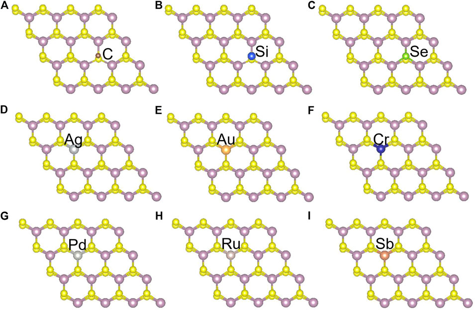
FIGURE 10. Monolayer 2H-MoS2 structure doped with different foreign atoms: (A–C) the substitution of a S atom with C, Si, and Se atoms, respectively; (D–I) the substitution of a Mo atom with Ag, Au, Cr, Pd, Ru, and Sb atoms, respectively.
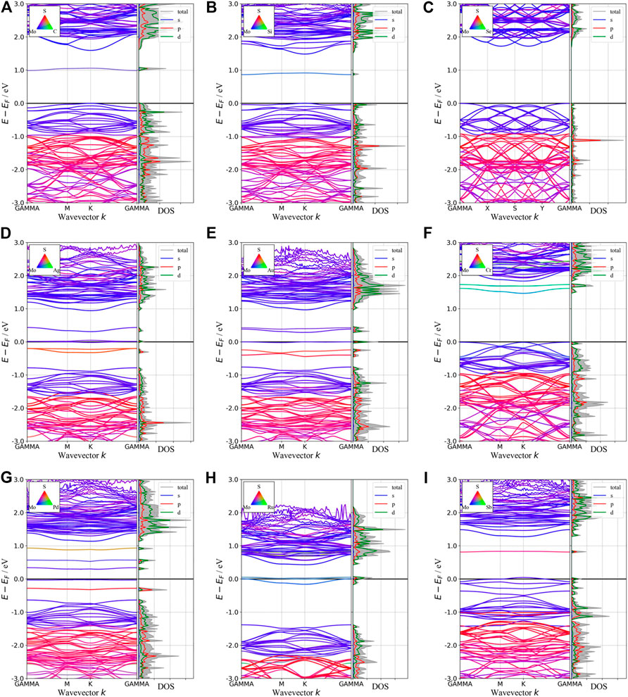
FIGURE 11. Band structures and pDOS of monolayer 2H-MoS2 after doping with different foreign atoms. The type of doped atoms is indicated by the color map in the upper left corner of each plot.
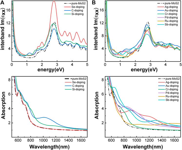
FIGURE 12. Optical properties of monolayer 2H-MoS2 after doping with different foreign atoms: (A) the imaginary part of the dynamic dielectric function; (B) absorption spectra. The left column is plotted for the substitution of S atom and the right for Mo atom. The black dotted line is for pure monolayer 2H-MoS2. The solid lines of different color refer to different doped atoms as shown in the legends.
Usually, the formation energy and the elastic stiffness constants are used to investigate the thermodynamic and mechanical stabilities of the system, respectively. To investigate the stability of the structure, we calculated the formation energy of all the structures with defects and those doping with foreign atoms, and the stiffness matrices of the three structures with defects that have good absorption performance in the NIR-II window, as shown in Figure 13. Considering that V-S1 has the lowest formation energy, it is the most common defect, which is consistent with the previous experiments (Zhou et al., 2013). Missing of the same number of S atoms is more stable than Mo atoms. Our calculations also show that the stability of the system becomes worse as the number of vacancies increases. In all the vacancies proposed in this study, single S, two S, and single Mo vacancies are relatively stable in either S-rich or Mo-rich environments. But Mo-vacancy is prone and easier to form under the condition of S-rich, and our calculation is the same as Feng’s conclusion (Feng et al., 2018). Combined with the ground-state energy, this indicates that V-S2-2, V-S2-6, and V-Mo1 are thermodynamically stable. As shown in Figure 13B, the foreign atoms doped on the monolayer MoS2 substrate are C, Si, and Se and Ag, Au, Cr, Pd, Ru, and Sb, respectively. However, in the case of Au, Ag, Pd, and Sb doping, substitutive doping has very high formation energy, so it is speculated that they may be more inclined to act as adsorbed atoms on the surface, which is consistent with the research of Wu et al (Wu et al., 2017). In addition, we found that the formation energy of different dopants substitution S-vacancy was lower than that substitution Mo-vacancy, which was consistent with our conclusion that the formation energy of Mo-vacancies was higher than that of S-vacancies.
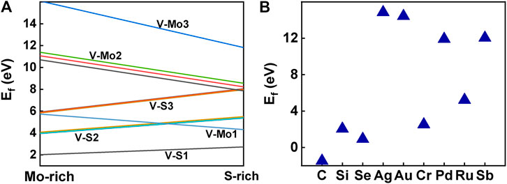
FIGURE 13. (A) Formation energies of different point defects, plot in Mo-rich and S-rich, which correspond to the chemical potential of its body-centered cubic bulk Mo and the S8 ring, respectively. (B) The doping formation energies of different foreign atoms.
In order to evaluate the mechanical stability of the point defects V-S2-2, V-S2-6, and V-Mo1, the elastic stiffness constants of the unit cell of the defects were calculated. For 2D materials, a necessary but not a sufficient condition for mechanical stability must be satisfied:
In conclusion, based on the first-principle calculations, we found that monolayer 1T-MoS2 has a better performance in the NIR-II absorption than that of the 2H phase. However, monolayer 2H-MoS2 has the advantage of stability over the 1T phase, and its NIR-II absorption can be improved by introducing vacancies, while doping with foreign atoms is less effective. Our results show that there exist stable double-S-vacancy configurations (V-S2-2 and V-S2-6) and single-Mo-vacancy configuration (V-Mo1) that can be applied in the NIR-II absorption. Our calculations provide a useful guideline for the fabrication of monolayer MoS2 for the purpose of photothermal therapy guided by photoacoustic imaging.
In this study, Vienna Ab initio Simulation Package (VASP) (Kresse and Furthmüller, 1996; Kresse and Furthmüller, 1996) has been used to calculate the electronic structure and optical properties of monolayer MoS2 films based on the projector augmented wave and Perdew–Burke–Ernzerhof (PAW-PBE) pseudopotential (Perdew et al., 1996; Kresse and Joubert, 1999). The numbers of valence electrons of each atom used in the calculation are listed in Table 2. The cutoff energy for plane wave expansion is set to be 500 eV. The generalized gradient approximation (GGA) is used for the exchange correlation energy functional to consider the nonuniformity of electron density. A vacuum layer of 15Å is taken in the z direction to avoid the interaction between the layers due to periodicity. The Brillouin zone integrations were carried out on the
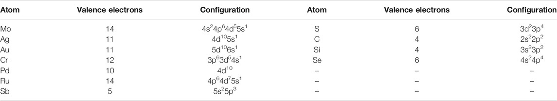
TABLE 2. Valence electrons of the atoms used in the calculation.
In addition, GW approximation (Shishkin and Kresse, 2006; Fuchs et al., 2007) is used to calculate the electron–electron scattering relaxation rate of 1T–metal phase monolayer MoS2. Combined with Drude-like intraband dielectric function contributions (Brendel and Bormann, 1992), the total dielectric function of 1T–metal phase MoS2 can be obtained. In the GW approximate calculation, the cutoff energy is set to be 300 eV, and 80eV is enough for the number of empty bands after the convergence test.
To investigate the formation of defects, the formation energy for defects can be calculated using the expression as follows (Persson et al., 2005):
where
where
The original contributions presented in the study are included in the article/Supplementary Material; further inquiries can be directed to the corresponding authors.
TL and XZ contributed to conception and design to the study. KY processed the calculation. All authors contributed to manuscript revision, read, and approved the submitted version.
The authors declare that the research was conducted in the absence of any commercial or financial relationships that could be construed as a potential conflict of interest.
The calculation was conducted on the High Performance Cluster at the Center for Joint Quantum Studies. This work was financially supported by the NSF of China (Nos. 11904256, 91859101, 81971744, U1932107, 82001952, and 81471786) and the Foundation of Tianjin University (1801).
Akhter, M. J., Kuś, W., Mrozek, A., and Burczyński, T. (2020). Mechanical Properties of Monolayer MoS2 with Randomly Distributed Defects. Materials 13 (6), 1307. doi:10.3390/ma13061307
Antaris, A. L., Chen, H., Cheng, K., Sun, Y., Hong, G., Qu, C., et al. (2016). A Small-Molecule Dye for NIR-II Imaging. Nat. Mater 15 (2), 235–242. doi:10.1038/nmat4476
Blöchl, P. E., Jepsen, O., and Andersen, O. K. (1994). Improved Tetrahedron Method for Brillouin-Zone Integrations. Phys. Rev. B 49 (23), 16223–16233. doi:10.1103/physrevb.49.16223
Brendel, R., and Bormann, D. (1992). An Infrared Dielectric Function Model for Amorphous Solids. J. Appl. Phys. 71 (1), 1–6. doi:10.1063/1.350737
Byrley, P., Liu, M., and Yan, R. (2019). Photochemically Induced Phase Change in Monolayer Molybdenum Disulfide. Front. Chem. 7, 442. doi:10.3389/fchem.2019.00442
Cazzaniga, M. (2012). GW and beyond Approaches to Quasiparticle Properties in Metals. Phys. Rev. B 86 (3), 035120. doi:10.1103/physrevb.86.035120
Chaste, J., Hnid, I., Khalil, L., Si, C., Durnez, A., Lafosse, X., et al. (2020). Phase Transition in a Memristive Suspended MoS2 Monolayer Probed by Opto- and Electro-Mechanics. ACS nano 14 (10), 13611–13618. doi:10.1021/acsnano.0c05721
Dumcenco, D. O., Kobayashi, H., Liu, Z., Huang, Y-S., and Suenaga, K. (2013). Visualization and Quantification of Transition Metal Atomic Mixing in Mo1− xWxS2 Single Layers. Nat. Commun. 4 (1), 1–5. doi:10.1038/ncomms2351
Fan, Y., Wang, P., Lu, Y., Wang, R., Zhou, L., Zheng, X., et al. (2018). Lifetime-engineered NIR-II Nanoparticles Unlock Multiplexed In Vivo Imaging. Nat. Nanotech 13 (10), 941–946. doi:10.1038/s41565-018-0221-0
Feng, L.-p., Sun, H.-q., Li, A., Su, J., Zhang, Y., and Liu, Z.-t. (2018). Influence of Mo-Vacancy Concentration on the Structural, Electronic and Optical Properties of Monolayer MoS2: A First-Principles Study. Mater. Chem. Phys. 209, 146–151. doi:10.1016/j.matchemphys.2018.01.015
Fuchs, F., Furthmüller, J., Bechstedt, F., Shishkin, M., and Kresse, G. (2007). Quasiparticle Band Structure Based on a Generalized Kohn-Sham Scheme. Phys. Rev. B 76 (11), 115109. doi:10.1103/physrevb.76.115109
Gajdoš, M., Hummer, K., Kresse, G., Furthmüller, J., and Bechstedt, F. (2006). Linear Optical Properties in the Projector-Augmented Wave Methodology. Phys. Rev. B 73 (4), 045112.
Geng, X., Sun, W., Wu, W., Chen, B., Al-Hilo, A., Benamara, M., et al. (2016). Pure and Stable Metallic Phase Molybdenum Disulfide Nanosheets for Hydrogen Evolution Reaction. Nat. Commun. 7 (1), 1–7. doi:10.1038/ncomms10672
Gordienko, A. B., and Filippov, S. I. (2009). A Modified Version of the Methfessel‒Paxton Method. Russ. Phys. J. 52 (7), 668–673. doi:10.1007/s11182-009-9281-9
Guan, S., Yang, S. A., Zhu, L., Hu, J., and Yao, Y. (2015). Electronic, Dielectric and Plasmonic Properties of Two-Dimensional Electride Materials X2N (X= Ca, Sr): A First-Principles Study. Sci. Rep. 5 (1), 1–14. doi:10.1038/srep12285
Gutiérrez, O. Y., Singh, S., Schachtl, E., Kim, J., Kondratieva, E., Hein, J., et al. (2014). Effects of the Support on the Performance and Promotion of (Ni)MoS2 Catalysts for Simultaneous Hydrodenitrogenation and Hydrodesulfurization. ACS Catal. 4 (5), 1487–1499. doi:10.1021/cs500034d
Harl, J. (2008). The Linear Response Function in Density Functional Theory: Optical Spectra and Improved Description of the Electron Correlation: Na.
Helveg, S., Lauritsen, J. V., Lægsgaard, E., Stensgaard, I., Nørskov, J. K., Clausen, B. S., et al. (2000). Atomic-Scale Structure of Single-LayerMoS2Nanoclusters. Phys. Rev. Lett. 84 (5), 951–954. doi:10.1103/physrevlett.84.951
Hong, G., Lee, J. C., Robinson, J. T., Raaz, U., Xie, L., Huang, N. F., et al. (2012). Multifunctional In Vivo Vascular Imaging Using Near-Infrared II Fluorescence. Nat. Med. 18 (12), 1841–1846. doi:10.1038/nm.2995
Hong, G., Robinson, J. T., Zhang, Y., Diao, S., Antaris, A. L., Wang, Q., et al. (2012). In Vivo Fluorescence Imaging with Ag2S Quantum Dots in the Second Near-Infrared Region. Angew. Chem. Int. Ed. 51 (39), 9818–9821. doi:10.1002/anie.201206059
Hong, J., Jin, C., Yuan, J., and Zhang, Z. (2017). Atomic Defects in Two-Dimensional Materials: From Single-Atom Spectroscopy to Functionalities in Opto-/Electronics, Nanomagnetism, and Catalysis. Adv. Mater. 29 (14), 1606434. doi:10.1002/adma.201606434
Imani Yengejeh, S., Liu, J., Kazemi, S. A., Wen, W., and Wang, Y. (2020). Effect of Structural Phases on Mechanical Properties of Molybdenum Disulfide. ACS omega 5 (11), 5994–6002. doi:10.1021/acsomega.9b04360
Jiao, L., Zhang, L., Wang, X., Diankov, G., and Dai, H. (2009). Narrow Graphene Nanoribbons from Carbon Nanotubes. Nature 458 (7240), 877–880. doi:10.1038/nature07919
Johari, P., and Shenoy, V. B. (2012). Tuning the Electronic Properties of Semiconducting Transition Metal Dichalcogenides by Applying Mechanical Strains. ACS nano 6 (6), 5449–5456. doi:10.1021/nn301320r
Kam, K. K., and Parkinson, B. A. (1982). Detailed Photocurrent Spectroscopy of the Semiconducting Group VIB Transition Metal Dichalcogenides. J. Phys. Chem. 86 (4), 463–467. doi:10.1021/j100393a010
Kan, M., Wang, J. Y., Li, X. W., Zhang, S. H., Li, Y. W., Kawazoe, Y., et al. (2014). Structures and Phase Transition of a MoS2 Monolayer. J. Phys. Chem. C 118 (3), 1515–1522. doi:10.1021/jp4076355
Komsa, H-P., Kotakoski, J., Kurasch, S., Lehtinen, O., Kaiser, U., and Krasheninnikov, A. V. (2012). Two-dimensional Transition Metal Dichalcogenides under Electron Irradiation: Defect Production and Doping. Phys. Rev. Lett. 109 (3), 035503. doi:10.1103/physrevlett.109.035503
Komsa, H-P., and Krasheninnikov, A. V. (2015). Native Defects in Bulk and Monolayer MoS2 from First Principles. Phys. Rev. B 91 (12), 125304. doi:10.1103/physrevb.91.125304
Kresse, G., and Furthmüller, J. (1996). Efficiency of Ab-Initio Total Energy Calculations for Metals and Semiconductors Using a Plane-Wave Basis Set. Comput. Mater. Sci. 6 (1), 15–50. doi:10.1016/0927-0256(96)00008-0
Kresse, G., and Furthmüller, J. (1996). Efficient Iterative Schemes Forab Initiototal-Energy Calculations Using a Plane-Wave Basis Set. Phys. Rev. B 54 (16), 11169–11186. doi:10.1103/physrevb.54.11169
Kresse, G., and Joubert, D. (1999). From Ultrasoft Pseudopotentials to the Projector Augmented-Wave Method. Phys. Rev. B 59 (3), 1758–1775. doi:10.1103/physrevb.59.1758
Kumar, A., and Ahluwalia, P. (2012). A First Principle Comparative Study of Electronic and Optical Properties of 1H–MoS2 and 2H–MoS2. Mater. Chem. Phys. 135 (2-3), 755–761. doi:10.1016/j.matchemphys.2012.05.055
Lahouij, I., Vacher, B., Martin, J-M., and Dassenoy, F. (2012). IF-MoS2 Based Lubricants: Influence of Size, Shape and crystal Structure. Wear 296 (1-2), 558–567. doi:10.1016/j.wear.2012.07.016
Li, H., Duan, X., Wu, X., Zhuang, X., Zhou, H., Zhang, Q., et al. (2014). Growth of Alloy MoS2xSe2(1-x)Nanosheets with Fully Tunable Chemical Compositions and Optical Properties. J. Am. Chem. Soc. 136 (10), 3756–3759. doi:10.1021/ja500069b
Liu, H., Hong, G., Luo, Z., Chen, J., Chang, J., Gong, M., et al. (2019). Atomic‐Precision Gold Clusters for NIR‐II Imaging. Adv. Mater. 31 (46), 1901015. doi:10.1002/adma.201901015
Mak, K. F., Lee, C., Hone, J., Shan, J., and Heinz, T. F. (2010). Atomically Thin MoS2: a New Direct-gap Semiconductor. Phys. Rev. Lett. 105 (13), 136805. doi:10.1103/physrevlett.105.136805
Mann, J., Ma, Q., Odenthal, P. M., Isarraraz, M., Le, D., Preciado, E., et al. (2014). 2-Dimensional Transition Metal Dichalcogenides with Tunable Direct Band Gaps: MoS2(1-x)Se2xMonolayers. Adv. Mater. 26 (9), 1399–1404. doi:10.1002/adma.201304389
Maździarz, M. (2019). Comment on ‘The Computational 2D Materials Database: High-Throughput Modeling and Discovery of Atomically Thin Crystals’. 2D Mater. 6 (4), 048001.
Monkhorst, H. J., and Pack, J. D. (1976). Special Points for Brillouin-Zone Integrations. Phys. Rev. B 13 (12), 5188–5192. doi:10.1103/physrevb.13.5188
Nakayasu, Y., Bradley, S., Kobayashi, H., Nayuki, K., Sasaki, Y., Tomai, T., et al. (2019). Rapid Synthesis of Defective and Composition-Controlled Metal Chalcogenide Nanosheets by Supercritical Hydrothermal Processing. Nanoscale Adv. 1 (9), 3383–3387. doi:10.1039/c9na00435a
Ogawa, S., and Petek, H. (1996). Femtosecond Dynamics of Hot-Electron Relaxation in Cu(110) and Cu(100). Surf. Sci. 357-358, 585–594. doi:10.1016/0039-6028(96)00228-2
Olmon, R. L., Slovick, B., Johnson, T. W., Shelton, D., Oh, S-H., Boreman, G. D., et al. (2012). Optical Dielectric Function of Gold. Phys. Rev. B 86 (23), 235147. doi:10.1103/physrevb.86.235147
Pan, J. W., Li, C., Zhao, Y. F., Liu, R. X., Gong, Y. Y., Niu, L. Y., et al. (2015). Electronic Properties of TiO2 Doped with Sc, Y, La, Zr, Hf, V, Nb and Ta. Chem. Phys. Lett. 628, 43–48. doi:10.1016/j.cplett.2015.03.056
Perdew, J. P., Burke, K., and Ernzerhof, M. (1996). Generalized Gradient Approximation Made Simple. Phys. Rev. Lett. 77 (18), 3865–3868. doi:10.1103/physrevlett.77.3865
Persson, C., Zhao, Y-J., Lany, S., and Zunger, A. (2005). n-Type Doping of CuInSe2 and CuGaSe2. Phys. Rev. B 72 (3), 035211. doi:10.1103/physrevb.72.035211
Rai, D. P., Vu, T. V., Laref, A., Ghimire, M. P., Patra, P. K., Srivastava, S., et al. (2020). Electronic and Optical Properties of 2D Monolayer (ML) MoS2 with Vacancy Defect at S Sites. Nano-Structures & Nano-Objects 21, 100404. doi:10.1016/j.nanoso.2019.100404
Schöne, W-D. (2007). Theoretical Determination of Electronic Lifetimes in Metals. Prog. Surf. Sci. 82 (4-6), 161–192. doi:10.1016/j.progsurf.2007.03.004
Shishkin, M., and Kresse, G. (2006). Implementation and Performance of the Frequency-dependent GW Method within the PAW Framework. Phys. Rev. B 74 (3), 035101. doi:10.1103/physrevb.74.035101
Shishkin, M., and Kresse, G. (2007). Self-consistent G W Calculations for Semiconductors and Insulators. Phys. Rev. B 75 (23), 235102. doi:10.1103/physrevb.75.235102
Soares, D. M., Mukherjee, S., and Singh, G. (2020). TMDs beyond MoS 2 for Electrochemical Energy Storage. Chem. Eur. J. 26 (29), 6320–6341. doi:10.1002/chem.202000147
Steinhoff, A., Kim, J.-H., Jahnke, F., Rösner, M., Kim, D.-S., Lee, C., et al. (2015). Efficient Excitonic Photoluminescence in Direct and Indirect Band Gap Monolayer MoS2. Nano Lett. 15 (10), 6841–6847. doi:10.1021/acs.nanolett.5b02719
Sun, C., Li, B., Zhao, M., Wang, S., Lei, Z., Lu, L., et al. (2019). J-aggregates of Cyanine Dye for NIR-II In Vivo Dynamic Vascular Imaging beyond 1500 Nm. J. Am. Chem. Soc. 141 (49), 19221–19225. doi:10.1021/jacs.9b10043
Wang, Q. H., Kalantar-Zadeh, K., Kis, A., Coleman, J. N., and Strano, M. S. (2012). Electronics and Optoelectronics of Two-Dimensional Transition Metal Dichalcogenides. Nat. Nanotech 7 (11), 699–712. doi:10.1038/nnano.2012.193
Wang, V., Xu, N., Liu, J. C., Tang, G., and Geng, W-T. (2019). VASPKIT: A User-Friendly Interface Facilitating High-Throughput Computing and Analysis Using VASP Code. doi:10.1002/leap.1229arXiv preprint arXiv:08269
Welsher, K., Liu, Z., Sherlock, S. P., Robinson, J. T., Chen, Z., Daranciang, D., et al. (2009). A Route to Brightly Fluorescent Carbon Nanotubes for Near-Infrared Imaging in Mice. Nat. Nanotech 4 (11), 773–780. doi:10.1038/nnano.2009.294
Wu, P., Yin, N., Li, P., Cheng, W., and Huang, M. (2017). The Adsorption and Diffusion Behavior of noble Metal Adatoms (Pd, Pt, Cu, Ag and Au) on a MoS2 Monolayer: a First-Principles Study. Phys. Chem. Chem. Phys. 19 (31), 20713–20722. doi:10.1039/c7cp04021k
Xu, D., Zhu, Y., Liu, J., Li, Y., Peng, W., Zhang, G., et al. (2016). Microwave-assisted 1T to 2H Phase Reversion of MoS2in Solution: a Fast Route to Processable Dispersions of 2H-MoS2nanosheets and Nanocomposites. Nanotechnology 27 (38), 385604. doi:10.1088/0957-4484/27/38/385604
Zeng, M., Liu, J., Zhou, L., Mendes, R. G., Dong, Y., Zhang, M.-Y., et al. (2020). Bandgap Tuning of Two-Dimensional Materials by Sphere Diameter Engineering. Nat. Mater. 19 (5), 528–533. doi:10.1038/s41563-020-0622-y
Zhang, X.-D., Wang, H., Antaris, A. L., Li, L., Diao, S., Ma, R., et al. (2016). Traumatic Brain Injury Imaging in the Second Near-Infrared Window with a Molecular Fluorophore. Adv. Mater. 28 (32), 6872–6879. doi:10.1002/adma.201600706
Zhang, X., Luster, B., Church, A., Muratore, C., Voevodin, A. A., Kohli, P., et al. (2009). Carbon Nanotube−MoS2 Composites as Solid Lubricants. ACS Appl. Mater. Inter. 1 (3), 735–739. doi:10.1021/am800240e
Zhou, W., Zou, X., Najmaei, S., Liu, Z., Shi, Y., Kong, J., et al. (2013). Intrinsic Structural Defects in Monolayer Molybdenum Disulfide. Nano Lett. 13 (6), 2615–2622. doi:10.1021/nl4007479
Keywords: monolayer MoS2, point defects, electronic structure, dielectric function, absorption, near-infrared-II
Citation: Yang K, Liu T and Zhang X-D (2021) Bandgap Engineering and Near-Infrared-II Optical Properties of Monolayer MoS2: A First-Principle Study. Front. Chem. 9:700250. doi: 10.3389/fchem.2021.700250
Received: 25 April 2021; Accepted: 27 May 2021;
Published: 18 June 2021.
Edited by:
Guohua Jia, Curtin University, AustraliaReviewed by:
Yunguo Li, University of Science and Technology of China, ChinaCopyright © 2021 Yang, Liu and Zhang. This is an open-access article distributed under the terms of the Creative Commons Attribution License (CC BY). The use, distribution or reproduction in other forums is permitted, provided the original author(s) and the copyright owner(s) are credited and that the original publication in this journal is cited, in accordance with accepted academic practice. No use, distribution or reproduction is permitted which does not comply with these terms.
*Correspondence: Tianyu Liu, dGlhbnl1X2xpdUB0anUuZWR1LmNu; Xiao-Dong Zhang, eGlhb2Rvbmd6aGFuZ0B0anUuZWR1LmNu
Disclaimer: All claims expressed in this article are solely those of the authors and do not necessarily represent those of their affiliated organizations, or those of the publisher, the editors and the reviewers. Any product that may be evaluated in this article or claim that may be made by its manufacturer is not guaranteed or endorsed by the publisher.
Research integrity at Frontiers
Learn more about the work of our research integrity team to safeguard the quality of each article we publish.