 Xin Yong
 Xiangchao Ma
 Weiming He
- School of Physics and Optoelectronic Engineering, Xidian University, Xi’an, China
Developing efficient N2 and O2 gas sensors is of great importance to our daily life and industrial technology. In this work, first-principles calculations are performed to study the N2 and O2 gas-sensing properties of pure and defected PtSe2. It is found that both N2 and O2 adsorb weakly on pure PtSe2, and adsorption of the molecules induces negligible changes in the electrical and optical properties. Whereas the Pt@Se anti-site defect significantly improves the N2 adsorption capacity of PtSe2 and induces notable changes in the electrical property. Similar results are also observed for the Pt and Se vacancies and Pt@Se anti-site defects when examining O2 adsorption. In addition, notable changes in the optical absorption spectra of the PtSe2 with Pt@Se defect are induced upon N2 adsorption, which also occurs for PtSe2 with Pt and Se vacancies and Pt@Se anti-site defects upon O2 adsorption. These results demonstrate that PtSe2 with the corresponding defects can be both excellent electrical and optical sensors for detecting N2 and O2 gases. Our work offers a new avenue for preparing efficient gas sensors.
Introduction
Oxygen is not only essential to the lives of humans and animals but also the key to the combustion-dependent processes such as power generation, chemical compound production, and heating. Controlling the air-to-fuel ratio during the combustion process at the critical point of excess oxygen is beneficial for improving the combustion efficiency, product generation, and safe combustion (Shuk and Jantz, 2015; Zhang et al., 2017). Because the presence of O2 corrodes gas storage and transportation systems, monitoring O2 in biomethane is also a necessary part (Urriza-Arsuaga et al., 2019). In the medical and food processing and waste management industries, sometimes it is also necessary to measure the oxygen content (Hong et al., 2018; Wang et al., 2019). Therefore, an efficient sensor for detecting O2 molecules plays an important role in modern technology. On the other hand, biogas is believed to be a promising substitute for natural gas due to its high methane content. However, the presence of impurity gas like N2 leads to a lower heating value. In addition, fuel dilution with N2 gas is generally used to reduce heat radiation, which is one of the main factors limiting the efficiency of gas turbines and internal combustion engines. Therefore, in order to meet the quality specifications, it is also necessary to detect and control N2 gas (Yi et al., 2013).
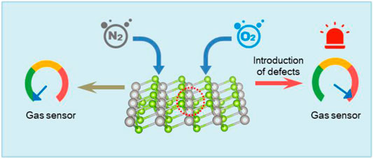
GRAPHICAL ABSTRACT
The generally used O2 and N2 gas sensors can be classified as electrical sensors and optical sensors according to the sensing principles: First, each kind of sensor requires efficient adsorption of the targeting gas molecules on the sensing material. For an electrical sensor, prominent charge transfer between the gas molecules and sensing material or charge trapping upon molecule adsorption converts the adsorption of gas molecules into electrical signal for detection. For an optical sensor, the adsorption of gas molecules notably alters the optical absorption spectrum of the sensing material. Traditionally, gas-sensing materials are metal–oxide–semiconductors, such as TiO2, SnO2, and ZnO (Kumar et al., 2014; Ibrahim et al., 2016; Xia et al., 2016). Recently, because of the theoretically infinite volume-to-surface ratio, which can provide enough active gas adsorption sites, intense studies on the gas-sensing properties of two-dimensional monolayer materials are reported (Yue et al., 2013; Bui et al., 2015; Ma et al., 2016a; Ma et al., 2016b; Sajjad et al., 2017; Klement et al., 2018; Ma X. et al., 2018; Ma D. et al., 2018; Jin et al., 2019; Ma D. et al., 2019; Ma et al., 2021). In particular, the intrinsic excellent sensing properties of Pt element render the monolayer PtSe2 as one of the mostly examined 2D gas-sensing material (Zhao et al., 2020). For example, Muhammad Sajjad et. al. studied the gas sensitivity of monolayer PtSe2 to the toxic NO2, NO, NH3, and CO gases (Sajjad et al., 2017); Dachang Chen et. al. studied the potential of PtSe2 as a gas sensor to detect SF6 decompositions (Chen et al., 2018).
On the other hand, the intrinsic defects, which can significantly affect the chemical, electrical, optical, and magnetic properties of PtSe2, are also extensively investigated. For example, Junfeng Gao et. al. studied the atomic structures and thermodynamic stability of vacancy defects. The study of Husong Zheng et. al. shows that the intrinsic Pt vacancy, Se vacancy, and Se@Pt anti-site defects can widely exist in ultrathin layered PtSe2 (Zheng et al., 2019); Ahmet Avsar et. al. found that Pt vacancy is responsible for the layer-dependent magnetism of PtSe2 (Avsar et al., 2019). In 2020, Jun Ge et. al. also reported the existence of magnetic moments induced by Pt vacancy defects in PtSe2 flakes (Ge et al., 2020).
Considering the ubiquity and easy introduction of intrinsic defects in PtSe2, in this work, we explore the N2 and O2 gas-sensing properties of both pure PtSe2 and PtSe2 with intrinsic defects, including Pt and Se vacancy defects (hereafter denoted as Pt-v and Se-v), Pt@Se and Se@Pt anti-site defects, and Pt and Se interstitial defects (hereafter denoted as Pt-inter and Se-inter), by first-principles calculations. It is found that PtSe2 with the Pt@Se anti-site defect has strong N2 adsorption capacity and exhibits significant change in the electrical properties upon N2 adsorption. Similar results are also observed for PtSe2 with Pt-v, Se-v, and Pt@Se defects when examining O2 adsorption. In addition, notable changes in the optical absorption spectra of the PtSe2 with Pt@Se defect are induced upon N2 adsorption, which also occurs for PtSe2 with Pt-v, Se-v, and Pt@Se upon O2 adsorption. These results demonstrate that PtSe2 with the corresponding defects can sensitively detect N2 and O2 molecules.
Computational Methods
The first-principles calculations are conducted using the Vienna Ab initio Simulation Package (VASP) (Kresse and Furthmüller, 1996). A cutoff energy of 400 eV is used for plane wave expansion, and the accuracy for self-consistent iteration is set to 10–5 eV. 4 × 4 supercells of pure PtSe2 are used for modeling the defected and molecules adsorbed on PtSe2, and the Brillouin zones for them are sampled with 3 × 3 × 1 gamma-centered k-points (Monkhorst and Pack, 1976). A vacuum layer larger than 30 Å is used for separating the atoms from their periodic images. For geometric optimization, the generalized gradient approximation (GGA) functional of Perdew–Burke–Ernzerhof is used (Perdew et al., 1996), and the atomic structures are fully relaxed until the residual forces on each atom are smaller than 0.02 eV/Å. To describe the interaction between the molecule and surface, DFT-D2 correction is used in the calculation. The more accurate HSE06 functional is used for calculating the electronic structures of pure and defected PtSe2 (Heyd et al., 2003). In order to quantify the electron charge redistribution between the adsorbed gas molecule and PtSe2, the Bader charge is analyzed based on the method of Henkelman (Henkelman et al., 2006; Sanville et al., 2007).
Results and Discussion
Adsorption Structures of Gas Molecules on Pure and Defected PtSe2
Adsorption of gas molecules on PtSe2 is an important parameter determining its gas-sensing properties. To establish the most stable adsorption structures of gas molecules on the monolayer, we first set many different configurations of gas molecules on the basal plane of PtSe2, which are then geometrically optimized. In this article, the Pt-v (Se-v) defect is formed by removing one Pt (Se) atom from a 4 × 4 supercell of pure PtSe2; the Pt@Se (Se@Pt) defect is formed by substituting Pt (Se) for Se (Pt), and the Pt-inter and Se-inter defects are formed by inserting Pt and Se atoms into the pure PtSe2. The structures with the largest adsorption energies are regarded as the most possible ones. The adsorption energy is defined as follows:
where
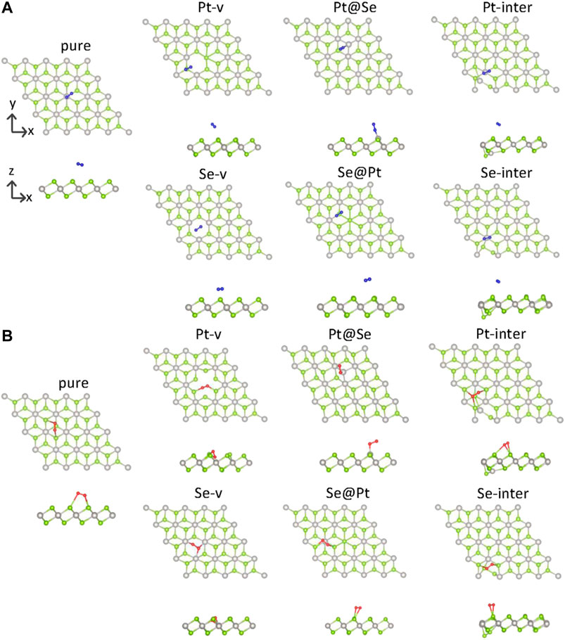
FIGURE 1. Top and side views of the adsorption structures of N2(A) and O2(B) on pure and defected PtSe2. The green and gray balls indicate Se and Pt atoms, respectively.
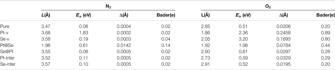
TABLE 1. Adsorption distance L (in Å), the absorption energy Ea (in eV), the change in the molecular bond length Δ (in Å) upon adsorption, and the values of Bader charges on molecules for the various adsorption structures.
To describe the bonding length of the molecules on the PtSe2 surface, we define the adsorption distance L as the closest distance between the atoms of gas molecules and the surface atoms. As shown in Figure 1; Table 1, it is observed that the N2 molecule bonds with the surface Se atom of pure PtSe2 and the adsorption distance and absorption energy is, respectively, 3.47 Å and 0.08 eV, which is similar to the vdW interaction length between Se and N atoms. This indicates that N2 adsorbs on the surface by very weak vdW force. For the PtSe2 with Pt-v defect, N2 still bonds with the surface Se atom and the absorption energy becomes about 1.83 eV, which is much larger than that on pure PtSe2. This is because the atomic structures around the Pt-v defect change significantly upon adsorption of N2, which releases a significant amount of energy as will be discussed in later section. However, the adsorption distance is as long as 3.68 Å. For PtSe2 with Pt@Se anti-site defect, N2 adsorbs on the surface by forming N–Pt bond, and the bond length and absorption energy are, respectively, 1.98 Å and 0.61 eV, which is within the sum of atomic radii of N and Pt (2.33 Å), indicating chemical interaction between them. For PtSe2 with Se-v, Se@Pt, Pt-inter, and Se-inter defects, the N2 molecule still bonds with the surface Se atom and the adsorption energies are only slightly larger than those on pure PtSe2, and the adsorption distances are between 3.5 and 3.6 Å. Therefore, the interaction between these defected structures and N2 molecule is of the vdW nature.
As shown in Figure 1B; Table 1, O2 bonds with the surface Se atoms of pure PtSe2, and the corresponding adsorption distance and adsorption energy are, respectively, 2.85 Å and 0.51 eV, which is larger than the lengths of any chemical bonds between O and Se. This indicates that O2 adsorbs on the surface mainly by vdW force. For PtSe2 with Pt-v defect, the adsorption distance becomes 1.86 Å, which is similar to the sum of covalent radii of O and Se (1.89 Å), and the absorption energy is as large as 2.36 eV. This indicates that O2 is chemically bonded to the surface. For PtSe2 with Se-v and Pt@Se defects, the O2 molecule is bonded to the surface by forming one or more Pt–O chemical bonds, and the adsorption energies are, respectively, 3.20 and 1.98 eV, and the bond lengths are, respectively, 2.05 and 1.92 Å, which is smaller than the sum of atomic radii of O and Pt (2.25 Å). Notably, as shown in Figure 1B, the O2 molecule is deeply embedded in the vacancy sites of PtSe2 with Pt-v and Se-v defects, indicating strong adsorption of O2 on the surfaces. For PtSe2 with Se@Pt, Pt-inter, and Se-inter defects, O2 still bonds with the surface Se atom, and the adsorption energies are only slightly larger than those on the pure surface and the adsorption distances are between 2.60 and 2.91 Å. Therefore, the interaction between these defect structures and O2 molecules is of vdW nature.
From the above results, it is noted that O2 and N2 molecules only weakly adsorb on the pure PtSe2, while all the intrinsic defects enhance more or less the interaction between the gas molecules and PtSe2. In particular, the Pt@Se anti-site defect transforms the initially weak vdW interaction into a strong chemical interaction between the molecules and PtSe2, and the Pt-v and Se-v defects also result in strong chemical interactions between O2 and PtSe2. In addition, O2 adsorbs more strongly than N2 on both the pure and defected PtSe2. These results are also supported by the changes in the molecular bond lengths and the Bader charges on the molecules, as listed in Table 1.
Charge Transfer and Electronic Structures of Gas Molecules on Pure and Defected PtSe2
Prominent charge transfer between the gas molecules and PtSe2 upon molecule adsorption is a fundamental prerequisite for transforming the existence of a gas molecule into electrical signal during gas-sensing application. To investigate the charge transfer between them, the Bader charge on molecules and charge density difference (CDD) for the molecule adsorbed on pure and defected PtSe2 are calculated and shown in Figure 2. The CCD is calculated according to the following equation:
where
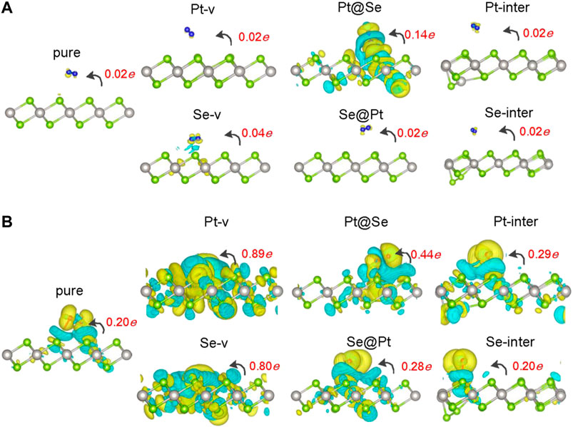
FIGURE 2. Charge density difference (CDD) for N2(A) and O2(B) adsorbed pure and defected PtSe2. The yellow (cyan) region represents charge accumulation (depletion), and the values of isosurfaces for all the structures are set to 0.0003 e/Å−3. The red numbers indicate the values of Bader charges on the molecules, and the black curved arrows indicate the orientation of charge transfer.
In order to understand the adsorption structures, charge transfer between molecules and PtSe2, and the charge trapping effects of the intrinsic defects shown above, we investigate the density of states (DOS) for pure and defected PtSe2 with the adsorption of gas molecules, the DOS of isolated N2 and O2 molecules, and the DOS of pure and defected PtSe2. As shown in Figure 3, the DOS of isolated N2 molecules shows that the 2π bonding orbital just lies under the Fermi level and has a lower height than 5σ orbital near −1 eV. The DOS of N2 basically still retains the characteristics of isolated N2 after adsorption on pure PtSe2 and PtSe2 with Pt-v, Se-v, Se@Pt, Pt-inter, and Se-inter defects, which is consistent with the weak interaction between N2 and pure and the defected PtSe2, whereas the DOS of N2 changes significantly upon the adsorption on PtSe2 with the Pt@Se anti-site defect. For example, the antibonding orbital of N2 near 4 eV splits into three peaks with lower height, and the relative values of the two bonding orbitals near −7.5 eV reverse, and they are in resonance with electronic states from PtSe2, indicating strong chemical interaction between N2 and PtSe2. In addition, because N2 bonds with the PtSe2 surface by forming Pt–N chemical bonds, the large electronegativity of N results in notable electron gain from Pt, which leads to the large value of Bader charge on N2. On the other hand, as shown in Figure 4, the electronic states near the valence band maximum (VBM) and conduction band minimum (CBM) are almost unchanged upon adsorption of N2 on pure PtSe2 and PtSe2 with Se-v, Se@Pt, Pt-inter, and Se-inter defects, whereas small gap states near both CBM and VBM appear upon adsorption of N2 on the PtSe2 with Pt@Se defect, which may additionally trap electrons and holes. These are consistent with the results of CDD shown above. For the PtSe2 with Pt-v defect, the atomic structures around the defect significantly change upon adsorption of N2, which introduces many gap states, as will be discussed in the following section.
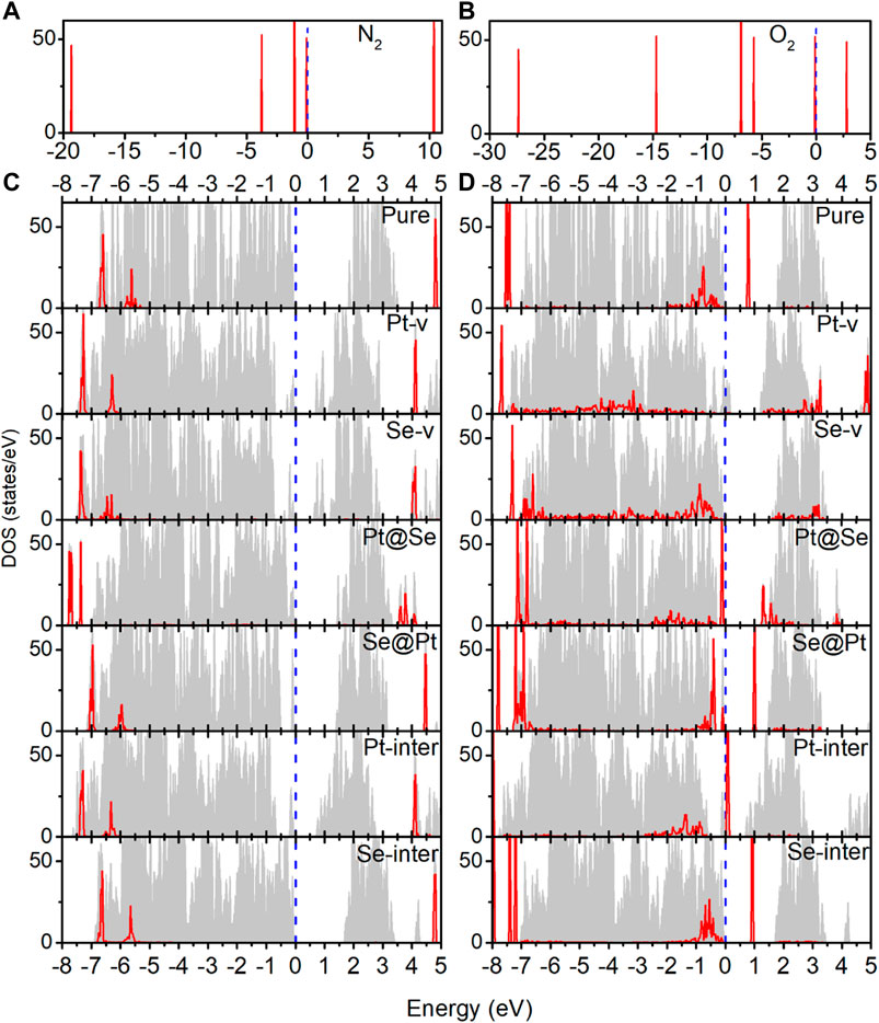
FIGURE 3. (A) Density of states (DOS) of the isolated N2 molecule. (B) DOS of the isolated O2 molecule. (C) DOS of pure and defected PtSe2 with the adsorption of N2. (D) DOS of pure and defected PtSe2 with the adsorption of O2. The gray areas indicate total DOS of the corresponding structures, and the red lines indicate projected DOS of the absorbed molecule. The values of DOS for adsorbed N2 and O2 on PtSe2 are set to 1.5 and 4 times for clear comparison. The Fermi levels (blue-dashed lines) for all the structures are set to 0 eV.
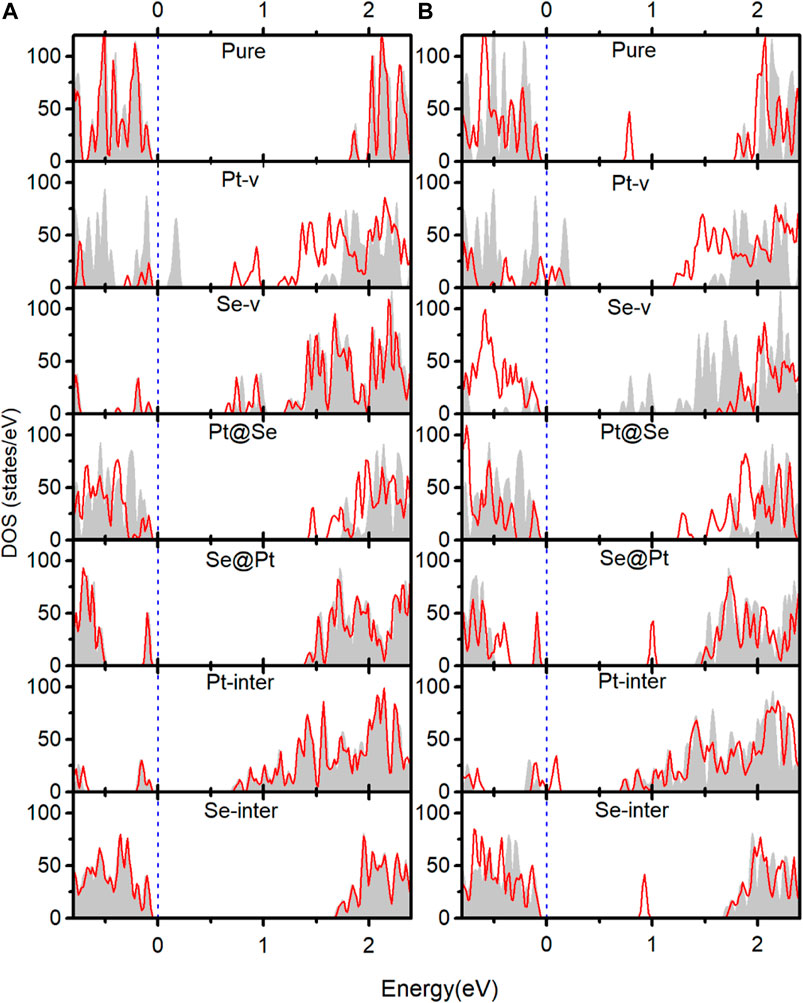
FIGURE 4. Red lines indicate the DOS near the band edges of pure and defected PtSe2 with the adsorption of N2(A) and O2(B). The gray areas indicate the DOS near band edges of pure and defected PtSe2.
As shown in Figure 3B, the DOS of isolated O2 shows five peaks lower than the Fermi level, and the 2π* antibonding orbital is the highest occupied orbital. The DOS of O2 hybridizes notably and to different extent with the DOS of PtSe2 upon adsorption on pure PtSe2 and defected PtSe2, and the hybridization is especially significant on PtSe2 with Pt-v, Se-v, and Pt@Se defects. These are consistent with the strong and different interactions between O2 and pure and defected PtSe2. Moreover, because O2 bonds with the PtSe2 surface by forming Pt (Se)–O vdW or chemical bonds, the large electronegativity of O results in notable electron gain, which leads to the large values of Bader charges on O2. On the other hand, as shown in Figure 4B, new electronic states near the VBM and CBM are introduced upon adsorption of O2 on pure PtSe2 and all the defected PtSe2, which may additionally trap electrons and holes. Therefore, significant redistribution of charge density around the defects occurs, as shown in the CDD of Figure 2B.
From the results above, it is noted that for N2, it is mainly the Pt@Se anti-site defect that can notably enhance the charge transfer between the gas molecules and PtSe2 and charge trapping states, while the other defects show negligible effects. For O2, all the defects, except Se-inter, enhance the charge transfer between the molecule and PtSe2, and the effects of Pt-v, Se-v, and Pt@Se defects are the most significant. In addition, the intrinsic defects introduce new electron and/or hole trapping states near the VBM and/or CBM. The charge transfer and charge trapping effects can result in significant electric signal when the defected PtSe2 is used as electrical sensors.
Optical Absorption Properties of Pure and Defected PtSe2 With Molecule Adsorption
The intrinsic defects and molecule adsorption not only affect the electronic structure and electrical properties of PtSe2 but may also affect its optical absorption properties. In order to study how they affect the optical properties of PtSe2, we calculated the optical absorption coefficients of pure and defected PtSe2 absorbed with N2 and O2. The specific calculation procedure is the same as one of our previous works (Ma X. et al., 2018; Ma X. et al., 2019; Yong et al., 2020; Jian et al., 2021). Figure 5 shows the optical absorption coefficients for polarization of E field along the in-plane x direction of pure and defected PtSe2 with and without the adsorption of N2 and O2. Note that the results for the polarization of E field along the in-plane y direction are almost the same as those along the in-plane x direction. As shown in Figure 5, for adsorption of N2, the optical absorption coefficients of pure PtSe2 and PtSe2 with Se-v, Se@Pt, Pt-inter, and Se-inter defects are basically the same as those of the structures without N2 adsorption. For the PtSe2 with Pt-v defect, there are two absorption peaks around 0.33 and 0.72 eV, whereas the adsorption of N2 eliminates these two absorption peaks and introduces a new and prominent absorption peak around 1.07 eV. For the PtSe2 with Pt@Se defect, the optical absorption edges are slightly extended to lower energy.
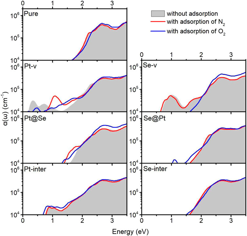
FIGURE 5. Optical absorption coefficients α(ω) of pure PtSe2 and defected PtSe2 with adsorption of N2 (red line) and O2 (blue line). The gray areas indicate the optical absorption coefficients of pure PtSe2 and defected PtSe2.
On the other hand, for adsorption of O2, the optical absorption coefficients of pure PtSe2 and PtSe2 with Pt-inter and Se-inter defects are roughly the same as those of the corresponding structures without adsorption. For the PtSe2 with Pt-v defect, the initial two absorption peaks around 0.33 and 0.72 eV are weakened and the absorption valley at 1.3 eV is filled upon the adsorption of O2. For the PtSe2 with Se-v defect, the notable absorption peak around 1.0 eV is quenched, and the optical absorption edge blue shifts significantly upon O2 adsorption. For PtSe2 with Pt@Se and Se@Pt defects, the optical absorption edges, mainly red shift slightly upon O2 adsorption. The notable changes in the absorption coefficients of defected PtSe2 upon N2 and O2 adsorption further verify the significant interactions between them and suggest that the characteristic changes in the optical spectra may be utilized for making high-performance and sensitive optical N2 and O2 gas detectors.
Special Results of Pt-v Defect Introduced by N2 Adsorption
Figure 6A shows the initial structures of the PtSe2 with Pt-v defect, which is formed by removing one of the Pt atoms in the supercell model and first-principles optimization. Upon N2 adsorption, the surrounding atomic structures of the Pt-v vacancy site change significantly, and these changes are retained when removing the adsorbed N2 molecule. As shown in Figure 6B, the upper Se atom closest to the defect site moves to the original position of Pt vacancy and bonds with the surrounding Se atoms. To characterize the differences in the properties of the two structures, the electronic structure and optical properties of them are calculated and shown in Figures 6C,D. As can be seen, the introduced gap states and the DOS near the valence band edge are very different for the two structures. The initial Pt-v structure introduces both occupied and unoccupied gap states near the valence band edge, whereas the new Pt-v structure introduces occupied gap states near the valence band edge and unoccupied gap states near the conduction band edge, thus exhibiting very different electrical properties. Because of this, the optical absorptions of them also show different characteristics. As shown in Figure 6D, the gray area shows that there are two absorption peaks around 0.33 and 0.72 eV, resulting from the gap states near the Fermi level, and there is an absorption valley at 1.3 eV. For the new Pt-v structure, there is mainly a characteristic absorption peak at 1.1 eV, resulting from the transition between gap states. The different optical absorption properties of the two structures may be used to differentiate the specific atomic structures of the Pt-v defect. The recent studies have shown that in few-layer PtSe2 flakes, the Pt vacancy defect on the surface and inside can produce localized magnetic moments. The versatile properties of Pt-v and easy tunability of Pt-v with the adsorption of N2 revealed here may be used to understand and tune the magnetic properties of PtSe2.
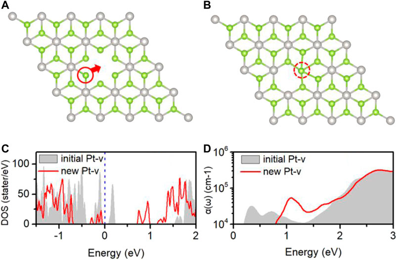
FIGURE 6. (A) Local atomic structures of the initial (A) and new (B) Pt-v defects; the DOS (C) and optical absorption coefficient (D) of PtSe2 with the initial Pt-v defect (gray areas) and new Pt-v defect (red lines). The Fermi levels (blue dashed line) are set to 0 eV.
Conclusion
In conclusion, we have studied the N2 and O2 gas-sensing properties of monolayer PtSe2 by characterizing the geometric structures, charge transfer, electronic structures, and the optical absorption of pure and defected PtSe2 with and without the adsorption of N2 and O2 molecules. It is found that both N2 and O2 adsorb weakly on pure PtSe2, whereas the Pt@Se anti-site defect significantly improves the N2 adsorption capacity of PtSe2 by converting the initial weak vdW interaction on pure PtSe2 into strong chemical interaction. Moreover, the defect not only promotes charge transfer from PtSe2 to N2 but also introduces charge trapping states around the defect, which leads to a significant change in the electrical properties of the structure. Similar results are also observed for the Pt-v, Se-v, and Pt@Se defects when examining O2 adsorption. In addition, a notable change in the optical absorption spectra of the PtSe2 with Pt@Se defect is induced upon N2 adsorption, and this also occurs for PtSe2 with Pt-v, Se-v, and Pt@Se upon O2 adsorption. Therefore, PtSe2 with the corresponding defects are promising materials for preparing sensitive electrical and optical sensors for detecting N2 and O2 molecules. Our work demonstrates the important role of intrinsic defects in improving and extending the sensing performance of PtSe2, which may be generalized to other materials.
Surprisingly, it is also found that significant changes in the atomic structures around Pt vacancy defect are induced upon adsorption of N2, which results in very different electronic and optical properties. The versatile properties of Pt vacancy and easy tunability with N2 molecules revealed here may have potential application for understanding and tuning the recently reported magnetic properties of PtSe2.
Data Availability Statement
The original contributions presented in the study are included in the article/Supplementary Material, and further inquiries can be directed to the corresponding author.
Author Contributions
XM conceived the basic idea. XY and WH did the implementation and ran the simulations. XY, XM, and JZ analyzed the results and wrote the manuscript.
Funding
This work is supported by the National Natural Science Foundation of China (11704298), the Postdoctoral Science Foundation of China (2019M653549), and the 2018 Postdoctoral Innovation Talent Support Program of China (BX20180233).
Conflict of Interest
The authors declare that the research was conducted in the absence of any commercial or financial relationships that could be construed as a potential conflict of interest.
References
Avsar, A., Ciarrocchi, A., Pizzochero, M., Unuchek, D., Yazyev, O. V., and Kis, A. (2019). Defect Induced, Layer-Modulated Magnetism in Ultrathin Metallic PtSe2. Nat. Nanotechnol. 14, 674–678. doi:10.1038/s41565-019-0467-1
Bui, V. Q., Pham, T.-T., Le, D. A., Thi, C. M., and Le, H. M. (2015). A First-Principles Investigation of Various Gas (CO, H2O, NO, and O2) Absorptions on a WS2 Monolayer: Stability and Electronic Properties. J. Phys. Condens. Matter. 27, 305005. doi:10.1088/0953-8984/27/30/305005
Chen, D., Zhang, X., Tang, J., Cui, Z., Cui, H., and Pi, S. (2018). Theoretical Study of Monolayer PtSe2 as Outstanding Gas Sensor to Detect SF6 Decompositions. IEEE Electron. Device Lett. 39, 1405–1408. doi:10.1109/LED.2018.2859258
Ge, J., Luo, T., Lin, Z., Shi, J., Liu, Y., Wang, P., et al. (2020). Magnetic Moments Induced by Atomic Vacancies in Transition Metal Dichalcogenide Flakes. Adv. Mater. 33, 2005465. doi:10.1002/adma.202005465
Henkelman, G., Arnaldsson, A., and Jónsson, H. (2006). A Fast and Robust Algorithm for Bader Decomposition of Charge Density. Comput. Mater. Sci. 36, 354–360. doi:10.1016/j.commatsci.2005.04.010
Heyd, J., Scuseria, G. E., and Ernzerhof, M. (2003). Hybrid Functionals Based on a Screened Coulomb Potential. J. Chem. Phys. 118, 8207–8215. doi:10.1063/1.1564060
Hong, S., Shin, J., Hong, Y., Wu, M., Jang, D., Jeong, Y., et al. (2018). Observation of Physisorption in a High-Performance FET-type Oxygen Gas Sensor Operating at Room Temperature. Nanoscale 10, 18019–18027. doi:10.1039/C8NR04472D
Ibrahim, A. A., Umar, A., Kumar, R., Kim, S. H., Bumajdad, A., and Baskoutas, S. (2016). Sm2O3-doped ZnO Beech Fern Hierarchical Structures for Nitroaniline Chemical Sensor. Ceramics Int. 42, 16505–16511. doi:10.1016/j.ceramint.2016.07.061
Jian, C.-c., Zhang, J., He, W., and Ma, X. (2021). Au-Al Intermetallic Compounds: A Series of More Efficient LSPR Materials for Hot Carriers-Based Applications Than Noble Metal Au. Nano Energy 82, 105763. doi:10.1016/j.nanoen.2021.105763
Jin, C., Tang, X., Tan, X., Smith, S. C., Dai, Y., and Kou, L. (2019). A Janus MoSSe Monolayer: a Superior and Strain-Sensitive Gas Sensing Material. J. Mater. Chem. A. 7, 1099–1106. doi:10.1039/C8TA08407F
Klement, P., Steinke, C., Chatterjee, S., Wehling, T. O., and Eickhoff, M. (2018). Effects of the Fermi Level Energy on the Adsorption of O 2 to Monolayer MoS 2. 2d Mater. 5, 045025. doi:10.1088/2053-1583/aadc24
Kresse, G., and Furthmüller, J. (1996). Efficient Iterative Schemes Forab Initiototal-Energy Calculations Using a Plane-Wave Basis Set. Phys. Rev. B. 54, 11169–11186. doi:10.1103/PhysRevB.54.11169
Kumar, M., Kumar, A., and Abhyankar, A. C. (2014). SnO2 Based Sensors with Improved Sensitivity and Response‐recovery Time. Ceramics Int. 40, 8411–8418. doi:10.1016/j.ceramint.2014.01.050
Ma, X., Yong, X., Jian, C.-c., and Zhang, J. (2019). Transition Metal-Functionalized Janus MoSSe Monolayer: A Magnetic and Efficient Single-Atom Photocatalyst for Water-Splitting Applications. J. Phys. Chem. C. 123, 18347–18354. doi:10.1021/acs.jpcc.9b03003
Ma, D., Zhang, J., Li, X., He, C., Lu, Z., Lu, Z., et al. (2018). C3N Monolayers as Promising Candidates for NO2 Sensors. Sensors Actuators B: Chem. 266, 664–673. doi:10.1016/j.snb.2018.03.159
Ma, D., Zeng, Z., Liu, L., Huang, X., and Jia, Y. (2019). Computational Evaluation of Electrocatalytic Nitrogen Reduction on TM Single-, Double-, and Triple-Atom Catalysts (TM = Mn, Fe, Co, Ni) Based on Graphdiyne Monolayers. J. Phys. Chem. C. 123, 19066–19076. doi:10.1021/acs.jpcc.9b05250
Ma, D., Ju, W., Li, T., Zhang, X., He, C., Ma, B., et al. (2016a). Modulating Electronic, Magnetic and Chemical Properties of MoS2 Monolayer Sheets by Substitutional Doping with Transition Metals. Appl. Surf. Sci. 364, 181–189. doi:10.1016/j.apsusc.2015.12.142
Ma, D., Wang, Q., Li, T., He, C., Ma, B., Tang, Y., et al. (2016b). Repairing Sulfur Vacancies in the MoS2 Monolayer by Using CO, NO and NO2 Molecules. J. Mater. Chem. C. 4, 7093–7101. doi:10.1039/C6TC01746K
Ma, D., Zeng, Z., Liu, L., and Jia, Y. (2021). Theoretical Screening of the Transition Metal Heteronuclear Dimer Anchored Graphdiyne for Electrocatalytic Nitrogen Reduction. J. Energ. Chem. 54, 501–509. doi:10.1016/j.jechem.2020.06.032
Ma, X., Wu, X., Wang, H., and Wang, Y. (2018). A Janus MoSSe Monolayer: a Potential Wide Solar-Spectrum Water-Splitting Photocatalyst with a Low Carrier Recombination Rate. J. Mater. Chem. A. 6, 2295–2301. doi:10.1039/C7TA10015A
Monkhorst, H. J., and Pack, J. D. (1976). Special Points for Brillouin-Zone Integrations. Phys. Rev. B. 13, 5188–5192. doi:10.1103/PhysRevB.13.5188
Perdew, J. P., Burke, K., and Ernzerhof, M. (1996). Generalized Gradient Approximation Made Simple. Phys. Rev. Lett. 77, 3865–3868. doi:10.1103/PhysRevLett.77.3865
Sajjad, M., Montes, E., Singh, N., and Schwingenschlögl, U. (2017). Superior Gas Sensing Properties of Monolayer PtSe2. Adv. Mater. Inter. 4, 1600911. doi:10.1002/admi.201600911
Sanville, E., Kenny, S. D., Smith, R., and Henkelman, G. (2007). Improved Grid-Based Algorithm for Bader Charge Allocation. J. Comput. Chem. 28, 899–908. doi:10.1002/jcc.20575
Shuk, P., and Jantz, R. (2015). Oxygen Gas Sensing Technologies: A Comprehensive Review9th International Conference on Sensing Technology (ICST). Auckland, New Zealand: IEEE, 12–17.
Urriza-Arsuaga, I., Bedoya, M., and Orellana, G. (2019). Luminescent Sensor for O2 Detection in Biomethane Streams. Sensors Actuators B: Chem. 279, 458–465. doi:10.1016/j.snb.2018.09.108
Wang, Y., Lai, X., Liu, B., Chen, Y., Lu, Y., Wang, F., et al. (2019). UV-induced Desorption of Oxygen at the TiO2 Surface for Highly Sensitive Room Temperature O2 Sensing. J. Alloys Compd. 793, 583–589. doi:10.1016/j.jallcom.2019.04.231
Xia, X., Wu, W., Wang, Z., Bao, Y., Huang, Z., and Gao, Y. (2016). A Hydrogen Sensor Based on Orientation Aligned TiO2 Thin Films with Low Concentration Detecting Limit and Short Response Time. Sensors Actuators B: Chem. 234, 192–200. doi:10.1016/j.snb.2016.04.110
Yi, H., Li, F., Ning, P., Tang, X., Peng, J., Li, Y., et al. (2013). Adsorption Separation of CO2, CH4, and N2 on Microwave Activated Carbon. Chem. Eng. J. 215-216, 635–642. doi:10.1016/j.cej.2012.11.050
Yong, X., Zhang, J., and Ma, X. (2020). Effects of Intrinsic Defects on the Photocatalytic Water-Splitting Activities of PtSe2. Int. J. Hydrogen Energ. 45, 8549–8557. doi:10.1016/j.ijhydene.2020.01.066
Yue, Q., Shao, Z., Chang, S., and Li, J. (2013). Adsorption of Gas Molecules on Monolayer MoS2 and Effect of Applied Electric Field. Nanoscale Res. Lett. 8, 425. doi:10.1186/1556-276X-8-425
Zhang, M., Xue, T., Xu, S., Li, Z., Yan, Y., and Huang, Y. (2017). Adverse Effect of Substrate Surface Impurities on O2 Sensing Properties of TiO2 Gas Sensor Operating at High Temperature. Ceramics Int. 43, 5842–5846. doi:10.1016/j.ceramint.2017.01.130
Zhao, X., Huang, R., Wang, T., Dai, X., Wei, S., and Ma, Y. (2020). Steady Semiconducting Properties of Monolayer PtSe2 with Non-metal Atom and Transition Metal Atom Doping. Phys. Chem. Chem. Phys. 22, 5765–5773. doi:10.1039/C9CP06249A
Keywords: gas sensing, electronic structures, optical properties, first-principles calculations, intrinsic defects
Citation: Yong X, Zhang J, Ma X and He W (2021) Efficient N2- and O2-Sensing Properties of PtSe2 With Proper Intrinsic Defects. Front. Chem. 9:676438. doi: 10.3389/fchem.2021.676438
Received: 05 March 2021; Accepted: 05 May 2021;
Published: 24 May 2021.
Edited by:
Guangzhao Wang, Yangtze Normal University, ChinaReviewed by:
Dongwei Ma, Anyang Normal University, ChinaYanan Tang, Zhengzhou Normal University, China
Copyright © 2021 Yong, Zhang, Ma and He. This is an open-access article distributed under the terms of the Creative Commons Attribution License (CC BY). The use, distribution or reproduction in other forums is permitted, provided the original author(s) and the copyright owner(s) are credited and that the original publication in this journal is cited, in accordance with accepted academic practice. No use, distribution or reproduction is permitted which does not comply with these terms.
*Correspondence: Xiangchao Ma, eGNtYUB4aWRpYW4uZWR1LmNu