 Qian Li
 Jinpeng Hu
 Yaru Cui*
95% of researchers rate our articles as excellent or good
Learn more about the work of our research integrity team to safeguard the quality of each article we publish.
Find out more
ORIGINAL RESEARCH article
Front. Chem. , 16 April 2021
Sec. Electrochemistry
Volume 9 - 2021 | https://doi.org/10.3389/fchem.2021.621549
This article is part of the Research Topic Design, Synthesis, and Modification of Metal Oxides for Energy Storage View all 12 articles
The copper–zinc–tin oxide (CZTO) precursor was synthesized to avoid sudden volume expansion from CZTO precursor to Cu2ZnSnS4 (CZTS) thin films and smooth CZTSSe thin-film surfaces without pinholes. The CZTO precursor was prepared by coprecipitation and ball milling to form nanoink of CZTO. Based on the CZTO precursor, the CZTS thin film was fabricated and then selenized to make pinhole-free and flat Cu2ZnSn(S,Se)4(CZTSSe) thin films. The results show that the CZTO precursor greatly contributed to elevating the homologous surface characteristics and crystallinity of CZTSSe thin films by controlling selenium temperature, selenium time, and selenium source temperature. Finally, the conversion efficiency of the CZTSSe thin-film solar cell fabricated from the CZTO precursor was 4.11%, with an open-circuit voltage (Voc) of 623 mV, a short circuit current density (Jsc) of 16.02 mA cm−2, and a fill factor (FF) of 41.2%.
In recent years, with the emergence of environmental problems and resource depletion, more scholars have paid their attention to green and sustainable materials and devices (Ali et al., 2019; Sharma et al., 2019). Cu2ZnSnS4(CZTS) is nontoxicity with elements, low cost, pollution-free, excellent bandgap (1.4–1.5 eV), and absorption coefficient (104/cm) (Wen et al., 2015; Kumar et al., 2018; Sun R. et al., 2019). Due to those advantages, CZTS thin-film material has attracted extensive attention. Up to now, CZTS thin films have been prepared by many methods such as sol–gel technique (Abdolahzadeh Ziabari et al., 2020), electrodeposition (Pawar et al., 2010), chemical bath deposition (Wang and Gong, 2011), and electrospinning technique (Ennaoui et al., 2009).
However, the direct generation of Cu2ZnSnS4(CZTS) using Cu–Zn–Sn(CZT) is always accompanied by the appearance of a secondary phase and defects, which make the morphology of thin film worse (Yoo et al., 2012). It was found that the preparation of CZTS with the copper–zinc–tin oxide (CZTO) precursor could effectively improve the morphology and smooth the surface of the thin film, and O atoms can be completely replaced by S atoms after the sulfidation procedure without residual oxide impurities (Ishino et al., 2013; Liu et al., 2018).
On the other hand, the semiconductor materials still present several defects such as large volume resistivity, defect density, and lower short circuit current (Jsc) causing poor device performance (Li et al., 2020). Tang prepared CZTS thin films by coprecipitation method, but the conversion efficiency was only 1.22% (Tang et al., 2013). Dong formed the CZTS absorption layer by simple sol–gel spin coating on Mo glass sheet, and the conversion efficiency of the solar cell was 2.25% (Dong et al., 2017). In order to prepare solar cells with high efficiency, Se doping is usually used to promote the growth of thin films (Chen et al., 2018). Chawla synthesized CZTSSe by high temperature arrested precipitation method (Chawla et al., 2018), with the increase of Se/S ratio, the degree of crystallization increases, and the calculated bandgap value was close to the optimal value of the solar photovoltaic conversion. Jin prepared CZTSSe thin films with CZTO as a precursor, the CZTO particles ensure the homogeneous distribution, and the conversion efficiency of 4.94% was achieved (Jin et al., 2016).
In this study, the CZTO precursor was introduced to reduce volume expansion of the thin film, inhibit the formation of the second phase, and also improve the property of thin-film solar cells. A smooth surface of a CZTSSe thin film without pinholes was obtained by annealing the CZTO precursor profiting for atoms’ entry into the precursor and improving crystal growth. The effects of controlling annealing temperature, holding time, and selenium source temperature on the microstructure and phases of CZTSSe thin films were studied providing a theoretical basis for the preparation of thin-film solar cells with low cost and high performance.
In a typical procedure, copper sulfate, zinc sulfate, and stannic sulfate were added with surfactant-increasing and pH-regulating method; the obtained Cu–Zn–Sn hydroxide was gathered and purified by filtration using DI water and ethanol three times and then calcined at 550°C to produce the CZTO nanoparticles. The mixture containing a certain amount of ethanol and CZTO nanoparticles was ball milled to form a nanoink, immediately, spinning on the Mo substrate to obtain the CZTO precursor thin film.
The CZTO thin film and sulfur powder were separately placed on the downstream side and the upstream side of the tube furnace. The sample was sulfide at 580°C for 1 h under Ar atmosphere with a heating rate of 10°C/min. Finally, the CZTS thin film was generated.
In order to optimize the performance of the thin film, the exceeded selenium powder and CZTS thin film were separately placed on the left side and right side of the tube furnace in the process of Se doping. The sample was selenized at 450°C for 1 h under Ar atmosphere with a heating rate of 10°C/min to obtain the desired CZTSSe thin film. In comparison, the annealing temperatures were 400, 500, 550, and 580°C, respectively, starting at different times of 0.5, 1.5, and 2 h and different Se source temperatures of 350, 400, and 450°C, respectively.
Solar cells with the structure Mo/CZTSSe/CdS/i-ZnO/ITO/Ag were fabricated. The N-type CdS layer was deposited on the CZTSSe layer by chemical bath method, and the i-ZnO and ITO windows layer were synthesized by RF magnetron sputtering and DC magnetron sputtering. Ag glue was pasted on top of the devices. Finally, the effective regions of the devices were 0.09 cm−2.
The characterization of the CZTSSe thin film from CZTO precursor prepared by different annealing parameters was implemented with several methods of measurement. The surface and cross-sectional morphologies of CZTO precursor and CZTSSe thin films were observed using field emission scanning electron microscopy (FESEM, NOVA450) at 20 kV. The elemental composition of the CZTSSe thin film was estimated using an X-ray energy spectrometer (EDS) attached to the FESEM and the thickness of the thin film was determined with a surface profiler (Veeco Dektak 150). The crystal structure of the CZTSSe thin film was analyzed by X-ray diffraction (XRD, Rigaku D/MAX-2000H) with CuKα radiation at 40 kV and 300 mA. To further confirm the crystallinity of the CZTSSe thin film, the phase was also performed using a Raman spectrometer (HR800-Horiba) with a laser excitation wavelength of 488 nm. The current–voltage (J-V) characteristics of CZTSSe solar cells were measured on an Oriel mode 94023 A measurement system.
Figure 1A shows the SEM image of the CZTO precursor thin film fabricated by spraying method with nanoink. The formed CZTO thin film by annealing owned good grain size and flat substrate. In the cross-sectional image of Figure 1B, the thickness of CZTO was approximately optimum, achieving perfect contact with Mo-based substrates without obvious void inside the membrane.
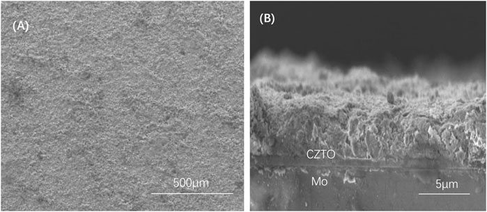
FIGURE 1. Surface SEM image (A) and cross-sectional SEM image (B) of CZTO precursor thin film.
The ratio of CZTSSe elements Cu/(Zn + Sn) was 1.02, 0.90, 1.04, 0.98, and 0.86 for the selenization temperature at 400, 450, 500, 550, and 580°C, and the ratio of Zn/Sn was 1.02, 0.90, 0.92, 1.01, and 0.84 at 400, 450, 500, 550, and 580°C, respectively. The data provide information that the sample keeps Cu-poor and Zn-rich compositions under 550°C of selenization temperature. On the one hand, Cu-poor condition causes more vacancies to be created and the concentration of shallow acceptor increased; besides, Zn-rich condition could restrain self-compensation defects and further improve the photoelectric conversion efficiency of CZTSSe thin-film solar cells (Chen et al., 2013; Sun L. et al., 2019).
Figure 2 shows the SEM images of CZTSSe surfaces at different selenization temperatures. As shown in Figures 2A,B, both CZTSSe particles exhibited small-sized crystals, suggesting that low substrate temperature was insufficient to form large-sized crystals. After annealing at 500°C, the CZTSSe particles can be clearly identified but showed an uneven distribution as shown in Figure 2C. The particle agglomeration of CZTSSe thin films was significantly reduced and CZTSSe demonstrated uniform distribution with an approximate size of 60 nm in Figure 2D at 550°C, indicating that the morphology of the thin film was improved. Nevertheless, after continuous heating to 580°C, the thin film was uneven again along with the loose surface.
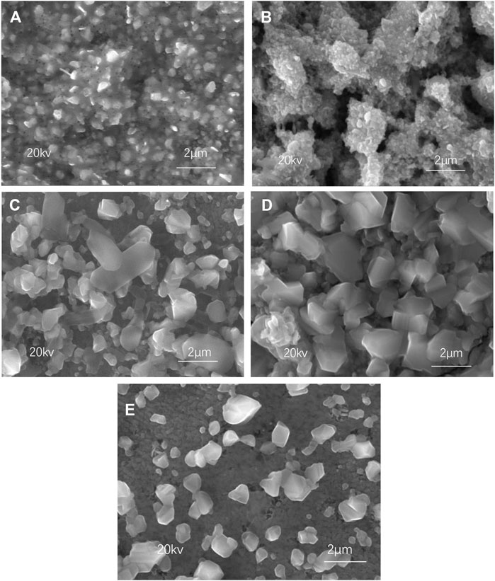
FIGURE 2. SEM images of CZTSSe thin films annealed at different temperatures: (A) 400°C, (B) 450°C, (C) 500°C, (D) 550°C, and (E) 580°C.
The XRD curves of CZTSSe thin films at different selenium temperatures are shown in Figure 3. Compared to the standard PDF cards (CZTS: JCPDS No. 26–0575 and CZTSe: JCPDS No. 52–0868), the three strong peaks in the figure can be completely matched, which proved the high crystallinity of CZTSSe (Ren et al., 2020; Sakul Bal et al., 2020). The diffraction peaks at 27.5°, 46.3°, and 54.1° were distinct and sharp at 400°C, and both peaks can be directed to the CZTS and CZTSe phase proving the presence of CZTSSe (Joshi et al., 2019). The diffraction peak had the smallest full width at half maximum when temperature arrived at 550°C, indicated of the best crystallinity. However, the secondary phases of MoSe2 and ZnSe appeared at 580°C, caused by the reaction of decomposition products of CZTS with Se and Mo substrate, resulting in a lower short circuit current. It was certificated that excessive temperature caused the formation of secondary phase resulting in material defect structure type and concentration hard to control.
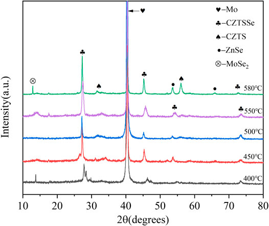
FIGURE 3. XRD patterns of CZTSSe thin films annealed at different temperatures 400, 450, 500, 550, and 580°C.
The Raman diagrams of CZTSSe thin films at different selenization temperatures are shown in Figure 4. The main peak of 336 cm−1 represented the generation of CZTS at 400°C (Khare et al., 2012; Kim et al., 2017). Raising at 450°C, the peak of CZTS was decreased and at the wavenumber of 192 cm−1 could be attributed to the CZTSSe phase. As the selenization temperature elevated, the vibration peak of CZTS disappeared, and the vibration signal intensity at 170 cm−1 and 192 cm−1 enhanced. It indicated that the entry of selenium into the lattice of CZTS increased the lattice constant and further caused the vibration peak of CZTS to move toward CZTSSe. In addition, the CZTSSe thin film annealed at 550°C showed sharper symmetrical vibration peaks around 170 cm−1 and 192 cm−1, and the vibration signal of CZTS disappeared near 336 cm−1. Corresponding to the CZTSSe phase, the transformation from CZTS to CZTSSe phase was achieved.
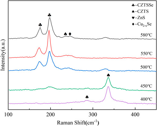
FIGURE 4. Raman spectra of CZTSSe thin films annealed at different temperatures 400, 450, 500, 550, and 580°C.
Table 1 shows the atomic ratios of CZTSSe thin films at different selenization holding times. The stoichiometric ratio of Cu/(Zn + Sn) and Zn/Sn had no significant changes during the annealing process, indicating that all the selenization time was unable to cause the metal atoms of thin films to volatilize. In addition, the ratio of S/(S + Se) had a tendency to decrease under the prolongation of holding time, which demonstrated that the more the selenium doping is, the more easy the CZTSSe particle generating is. However, the forbidden bandwidth of CZTSSe decreases with the increase of selenium content in the thin films. According to theoretical research, when S/(S + Se) approaches 0.2, the efficiency of theory conversion can be increased (Pakštas et al., 2020). We achieved this condition through 60 min selenization holding time.
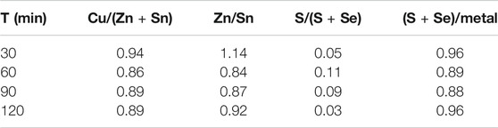
TABLE 1. Atomic ratios of CZTSSe thin films at different selenization holding times.
Figure 5 shows the SEM images of CZTSSe thin films at different holding times. It can be seen from Figure 5A that the morphology of CZTSSe nanoparticles had been changed to tetragonal crystal at 30 min of selenization holding time. The sample formed a regular crystal when the selenization holding time reached 60 min, which certificated the fulfillment of the selenization process. As shown in Figures 5B–D, with all slight deformation, the CZTSSe maintained a better original morphology and crystallinity under 60 min of selenization holding time, which may be assigned to an appropriate time for selenium preservation. Moreover, it can be seen from Figure 5C that the surface of CZTSSe thin films became rough derived from the deposition of excessive metal selenide due to long insulation time. Therefore, with reference to the analysis of the SEM images, 60 min was the best selenization holding time.
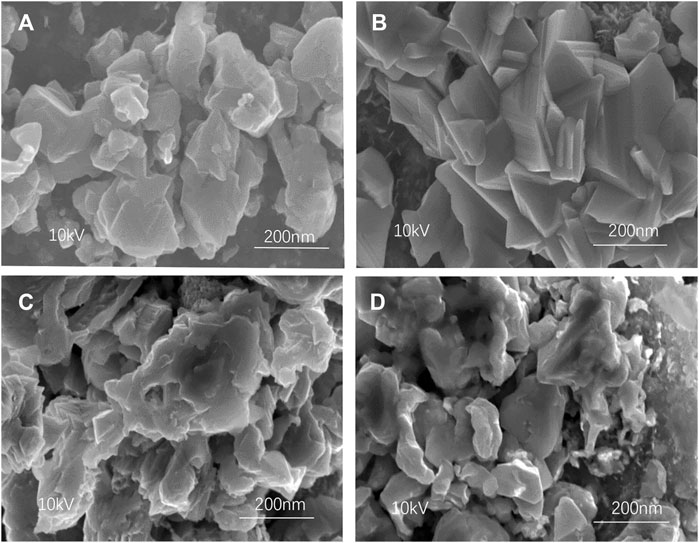
FIGURE 5. SEM images of CZTSSe thin films annealed at different times: (A) 30 min, (B) 60 min, (C) 90 min, and (D) 120 min.
Figure 6 shows the XRD patterns of CZTSSe thin films at different selenization holding times. By comparing standard PDF cards (CZTS: JCPDS No.26–0575 and CZTSe: JCPDS No.52–0868), the three strong peaks in the figure correspond to the card position, and the formation of CZTSSe can be initially determined. However, the second phase of Cu2S and ZnSe was obvious to be found at the selenium holding time of 30 min, which proved that Se atoms were not replaced by S atoms but formed hetero phases such as Cu2S and ZnSe.
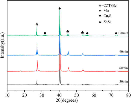
FIGURE 6. XRD patterns of CZTSSe thin films annealed at different times 30, 60, 90, and 120 min.
As can be seen from Figure 7, the vibration peak of 280 cm−1 did not disappear at 30 min, indicating the incomplete transformation from CZTS to CZTSSe; nevertheless, the vibrations of CZTSSe appeared at 173 cm−1 and 197 cm−1 (Kumar et al., 2018; Li et al., 2020). All of those proved the presence of residual CZTS; therefore, a large number of fine particles of CZTS still existed on the surface of the thin film. When the holding time reached above 60 min, the CZTS vibration peak disappeared; however, CuxSe and ZnS peaks appeared annealed at 90 and 120 min (Chalapathy et al., 2018; Kogler et al., 2019). It is worth considering that more selenium particles may be evaporated with prolongation of the selenium holding time, resulting in the appearance of impurity peaks. Therefore, the optimal selenization holding time was 60 min.
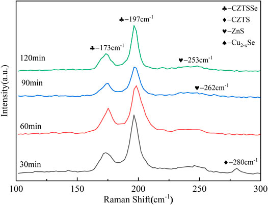
FIGURE 7. Raman spectra of CZTSSe thin films annealed at different times 30, 60, 90, and 120 min.
As shown in Table 2, the content of Cu was minimal when the temperature of the selenium source was 400°C, while the ratio of S/(S + Se) tends to increase with rising selenium source temperature, and the ratio is close to 0.2, which was beneficial to the formation of CZTSSe thin films (Pakštas et al., 2020).
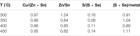
TABLE 2. Atomic ratios of CZTSSe thin films at different selenization source temperatures.
SEM images in Figure 8 show the CZTSSe surface following different selenium source temperatures, 300, 350, 400, and 450°C. As shown in Figures 8A,B, samples with a selenium source temperature of 300 and 350°C exhibited some trivial particles, demonstrating the agglomeration with a nonuniform surface. Also, the sample at 450°C showed decreased crystallinity as shown in Figure 8D, resulting in deterioration of film morphology and surface roughness. When the selenium source temperature arrived at 400°C, the surface of the thin film was evenly to form a crystalline substance with an approximate size of 85 nm, which can inhibit carrier recombination and further improve the device efficiency of CZTSSe thin-film solar cells (Ren et al., 2020).
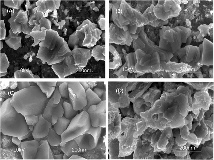
FIGURE 8. SEM images of CZTSSe thin films at different selenium source temperatures: (A) 300°C, (B) 350°C, (C) 400°C, and (D) 450°C.
XRD confirmed that all samples annealed at different selenium source temperatures were highly crystalline as shown in Figure 9. The peak intensity of thin films increased with rising selenium source temperature due to promoting crystallinity of CZTSSe thin films. However, a secondary phase such as ZnSe occurred again at 450°C reducing the conversion efficiency of the CZTSSe thin-film solar cell.
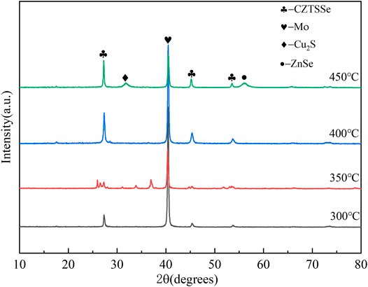
FIGURE 9. XRD patterns of CZTSSe thin films at different selenium source temperatures 300, 350, 400, and 450°C.
Figure 10 shows the Raman spectra for all samples. The Raman spectra of CZTSSe thin films under different selenium source temperatures showed obvious peaks at 170 cm−1 and 192 cm−1 associating with the main vibrational mode for single-phase CZTSSe. In addition, a weak peak appeared at 336 cm−1 at 300°C pointing to the residual of CZTS, and the weak of 336 cm−1 decreased following the increase of selenium source temperature. The above results indicated that Se doping into the CZTS lattice resulted in the migration of CZTS vibration peak to form CZTSSe. However, there were two distinct hetero peaks under the selenium source temperature at 450°C, certificating the formation of CuxSe and ZnS and further proving that excessive temperature of selenium source was not conducive to the composition of CZTSSe thin films. By studying the morphology, phase, and composition of CZTSSe thin films at different selenium source temperatures, it can be concluded that 400°C should be selected as the optimal temperature for the selenium source in the experiment.
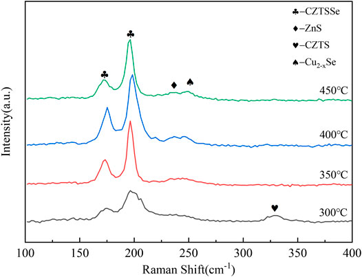
FIGURE 10. Raman spectra of CZTSSe thin films at different selenium source temperatures 300, 350, 400, and 450°C.
Figure 11A shows the SEM cross section of the CZTSSe thin-film solar cell prepared by CZTO precursor and then annealed CZTS to form the Cu2ZnSn(S,Se)4(CZTSSe) thin film. The CZTSSe thin film maintained a thickness of 1.8 μm, which was suitable for the transformation of light energy. The CZTSSe thin film presented a large grain with tight contact of interfacial layers and no visible grain boundaries or pores. CZTSSe solar cell device was fabricated with a Mo/CZTSSe/CdS/i-ZnO/ITO/Ag, and the J-V curve was shown in Figure 11B. The device demonstrated 4.11% photoelectric conversion efficiency (PCE) with an open-circuit voltage (Voc) of 623 mV, a short circuit current density (Jsc) of 16.02 mA cm−2, and a fill factor (FF) of 41.2%. The low electron and hole bonding rate may be related to the large grain size, smooth surface, and dense thin-film morphology. In addition, ZnO can conduct holes, and the N-type CdS layer has the role of electron transfer, which further improves the electron transport efficiency. However, it is possible to form a second phase particle at the back contact interface by calcination of selenium such as MoSe2; the existence of a secondary phase has a negative impact on the performance of the solar cell and not only increases the resistance but also losses the quality of devices. Therefore, the CZTSSe thin film synthesized with the CZTO precursor under an optimal condition can ensure the condition of Cu-poor and Zn-rich, inhibit the formation of the second phase, reduce the self-compensation defect, and further improve the conversion efficiency of solar cells.
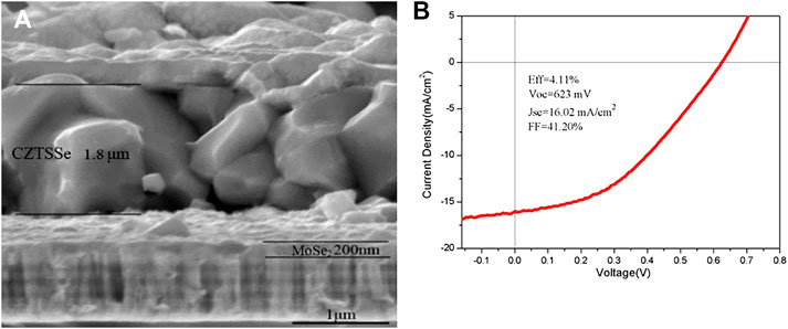
FIGURE 11. Cross section (A) and J-V curve (B) of CZTSSe thin-film solar cell.
In conclusion, the CZTO precursor can effectively promote the surface morphology of CZTSSe thin films. In the process of calcination, O atoms can be replaced by S atoms without any impurities creating high-quality CZTSSe thin films. It was revealed that the composition and morphology of the CZTO precursor played an important role in fabricating CZTSSe thin films with good crystallinity by controlling annealing temperature, holding time, and selenium source temperature. The CZTO precursor with suitable composition was obtained to regulate and control the formation of CZTSSe, which was confirmed by XRD, Raman, SEM, and EDX techniques. It was found that the peak of CZTSSe exists and becomes sharper with increasing calcination parameters (temperature, annealing time, and selenium source temperature). Raman curves proved the presence of CZTSSe thin films with two obvious peaks at 173 cm−1 and 197 cm−1; similar to the XRD test, the peak of CZTSSe also becomes stronger with the increase of annealing time. However, excessive or insufficient temperature and annealing times lead to the appearance of secondary phases such as ZnSn and CuxSe. SEM scanning showed the phase transition of the thin film under different conditions and proved that large particle size and smooth and compact surface of the thin film can improve the performance of the CZTSSe solar cell. According to EDX analysis, with the change of annealing parameters, the composition of Cu/(Zn + Sn), Zn/Sn, and S/(S + Se) also changed to a varying degree. It can be found that the more the doped Se is, the more the CZTSSe is generated. Also, the forbidden bandwidth of the CZTSSe thin film decreases with the increase of Se atoms in the membrane; thus, the conversion efficiency of the CZTSSe thin-film solar cell was improved with the condition of S/(S + Se) approaching 0.2, the annealed temperature of 550°C at 60 min, and selenium source temperature of 400°C. Moreover, CZTSSe thin-film solar cells based on the periods of fabrication of CZTO precursor and selenization of the CZTS thin film demonstrated the power conversion efficiency of 4.11% due to complete diffusion of S and Se atoms. In conclusion, these confirm the feasibility of using CZTO precursor for the preparation of highly efficient CZTSSe solar cells by further optimal progression.
The original contributions presented in the study are included in the article/Supplementary Material; further inquiries can be directed to the corresponding authors.
All authors listed have made substantial, direct, and intellectual contribution to the work and approved it for publication.
This work was supported by the National Natural Science Foundation of China (No. 51504181 and No. 51674186), Shanxi Natural Science Foundation (No. 2020JQ-679), Shanxi Key Laboratory Project (No. 20JS064), Key Laboratory Project of Xi’an (No. 2019219914SYS014CG036), and Innovation and Entrepreneurship Training Program of Xi'an University of Architecture and Technology in 2020 (No. S202010703126).
The authors declare that the research was conducted in the absence of any commercial or financial relationships that could be construed as a potential conflict of interest.
Abdolahzadeh Ziabari, A., Mohabbati Zindanlou, N., Hassanzadeh, J., Golshahi, S., and Bagheri Khatibani, A. (2020). Fabrication and study of single-phase high-hole-mobility CZTS thin films for PV solar cell applications: influence of stabilizer and thickness. J. Alloys Compd. 842, 155741. doi:10.1016/j.jallcom.2020.155741
Ali, A., Jacob, J., Ashfaq, A., Mahmood, K., Ahmad, S., Rehman, U., et al. (2019). Effect of tin concentration on the structural, optical and thermoelectric properties of CZTS thin films gown by chemical solution method. Ceram. Int. 45, 22513–22516. doi:10.1016/j.ceramint.2019.07.276
Chalapathy, R. B. V., Gang, M. G., Hong, C. W., Kim, J. H., Jang, J. S., Yun, J. H., et al. (2018). Performance of CZTSSe thin film solar cells fabricated using a sulfo-selenization process: influence of the Cu composition. Sol. Energy 159, 260–269. doi:10.1016/j.solener.2017.10.085
Chawla, P., Jain, S., Vashishtha, P., Ahamed, M., and Sharma, S. N. (2018). Transition from CZTSe to CZTS via multicomponent CZTSSe: potential low cost photovoltaic absorbers. Superlattices Microstruct. 113, 502–509. doi:10.1016/j.spmi.2017.11.025
Chen, C. Y., Aprillia, B. S., Chen, W. C., Teng, Y. C., Chiu, C. Y., Chen, R. S., et al. (2018). Above 10% efficiency earth-abundant Cu2ZnSn(S,Se)4 solar cells by introducing alkali metal fluoride nanolayers as electron-selective contacts. Nano Energy 51, 597–603. doi:10.1016/j.nanoen.2018.06.028
Chen, S., Walsh, A., Gong, X.-G., and Wei, S.-H. (2013). Classification of lattice defects in the kesterite Cu2ZnSnS4 and Cu2ZnSnSe4 earth-abundant solar cell absorbers. Adv. Mater. 25, 1522–1539. doi:10.1002/adma.201203146
Dong, L., Cheng, S., Lai, Y., Zhang, H., and Jia, H. (2017). Sol-gel processed CZTS thin film solar cell on flexible molybdenum foil. Thin Solid Films 626, 168–172. doi:10.1016/j.tsf.2017.02.019
Ennaoui, A., Lux-Steiner, M., Weber, A., Abou-Ras, D., Kötschau, I., Schock, H.-W., et al. (2009). Cu2ZnSnS4 thin film solar cells from electroplated precursors: novel low-cost perspective. Thin Solid Films 517, 2511–2514. doi:10.1016/j.tsf.2008.11.061
Ishino, R., Fukushima, K., and Minemoto, T. (2013). Improvement of Cu2ZnSnS4 thin film morphology using Cu-Zn-Sn-O precursor fabricated by sputtering. Curr. Appl. Phys. 13, 1861–1864. doi:10.1016/j.cap.2013.06.021
Jin, X., Yuan, C., Zhang, L., Jiang, G., Liu, W., and Zhu, C. (2016). Pulsed laser deposition of Cu2ZnSn(SxSe1−x)4 thin film solar cells using quaternary oxide target prepared by combustion method. Sol. Energy Mater. Sol. Cells 155, 216–225. doi:10.1016/j.solmat.2016.06.022
Joshi, R. A., Gupta, M., and Phase, D. M. (2019). Annealing induced modifications in physicochemical and optoelectronic properties of CdS/CuInGaSe2 thin film. Sol. Energy 177, 1–7. doi:10.1016/j.solener.2018.10.088
Khare, A., Himmetoglu, B., Johnson, M., J. Norris, D., Cococcioni, M., and Aydil, E. S. (2012). Erratum: “Calculation of the lattice dynamics and Raman spectra of copper zinc tin chalcogenides and comparison to experiments”. J. Appl. Phys. 111, 129901. doi:10.1063/1.4730607
Kim, Y. J., Jo, E. J., Kamble, A. S., Gang, M. G., Kim, J. H., Moon, J. H., et al. (2017). Improving the solar cell performance of electrodeposited Cu2ZnSn(S,Se)4 by varying the Cu/(Zn + Sn) ratio. Sol. Energy 145, 13–19. doi:10.1016/j.solener.2017.01.059
Kogler, W., Schnabel, T., Ahlswede, E., and Powalla, M. (2019). Study on formation and characterization of CZTSSe-based absorber layer from a green solution based approach. Sol. Energy Mater. Sol. Cells 200, 109959. doi:10.1016/j.solmat.2019.109959
Kumar, V., Padhy, S., Basak, A., and Singh, U. P. (2018). Effect of HCl and NH4OH etching on CZTSSe absorber layer. Vacuum 155, 336–338. doi:10.1016/j.vacuum.2018.06.038
Li, Y., Wang, S., Liao, H., Li, X., Xu, X., and Yang, S. (2021). Improvement of Cu2ZnSnS4 thin film performance by using oxygen-containing Cu-Zn-Sn precursor. Mater. Sci. Semicond. Process. 123, 105556. doi:10.1016/j.mssp.2020.105556
Li, Y., Zhang, H.-X., Zhao, Y., Dong, X.-F., Zheng, T.-T., and Wang, C.-W. (2020). Influence of the selenization condition on the properties of ambient-air processed CZTSSe thin films and device performance. Appl. Surf. Sci. 516, 145872. doi:10.1016/j.apsusc.2020.145872
Liu, X., Hao, R., Zhao, Q., Chang, F., Li, Y., Gu, K., et al. (2018). Studies on sputtered Cu-Zn-Sn-O precursor to fabricate Cu2ZnSnS4 thin films. J. Phys. Sci. 73, 957–964. doi:10.1515/zna-2018-0177
Pakštas, V., Grincienė, G., Kamarauskas, E., Giraitis, R., Skapas, M., Selskis, A., et al. (2020). Impact of CdS layer thickness on the composition, structure and photovoltaic performance of superstrate CZTSSe solar cells. Sol. Energy 207, 1231–1239. doi:10.1016/j.solener.2020.07.052
Pawar, B. S., Pawar, S. M., Shin, S. W., Choi, D. S., Park, C. J., Kolekar, S. S., et al. (2010). Effect of complexing agent on the properties of electrochemically deposited Cu2ZnSnS4 (CZTS) thin films. Appl. Surf. Sci. 257, 1786–1791. doi:10.1016/j.apsusc.2010.09.016
Ren, G. A., Zhuang, D. M., Zhao, M., Wei, Y. W., Wu, Y. X., Li, X. C., et al. (2020a). CZTSSe solar cell with an efficiency of 10.19% based on absorbers with homogeneous composition and structure using a novel two-step annealing process. Sol. Energy 207, 651–658. doi:10.1016/j.solener.2020.07.016
Ren, G., Zhuang, D., Zhao, M., Wei, Y., Wu, Y., Li, X., et al. (2020b). Influence of H2Se concentration on Se-rich CZTSSe absorbers sputtered with a ceramic quaternary target. Ceram. Int. 46, 13704–13710. doi:10.1016/j.ceramint.2020.02.158
Sakul Bal, S., Padhy, S., and Singh, U. P. (2020). Effect of Ge & ZnO inter-layer on the properties of CZTSSe absorber layer. Mater. Today Proc. 39, 1843–1847. doi:10.1016/j.matpr.2020.06.363
Sharma, S. D., Khasimsaheb, B., Chen, Y. Y., and Neeleshwar, S. (2019). Enhanced thermoelectric performance of Cu2ZnSnS4 (CZTS) by incorporating Ag nanoparticles. Ceram. Int. 45, 2060–2068. doi:10.1016/j.ceramint.2018.10.109
Sun, L., Shen, H., Huang, H., Raza, A., and Zhao, Q. (2019). Effect of evaporated Sb layer on performance of flexible CZTSSe thin film solar cell. Sol. Energy 193, 267–274. doi:10.1016/j.solener.2019.09.073
Sun, R., Zhuang, D., Zhao, M., Zhang, N., Xie, M., Wei, Y., et al. (2019). Phases formation of Cu2ZnSnS4 thin films by sulfurizing stacked precursors by sputtering from Cu Zn and Cu Sn targets. Thin Solid Films 690, 137561. doi:10.1016/j.tsf.2019.137561
Tang, D., Wang, Q., Liu, F., Zhao, L., Han, Z., Sun, K., et al. (2013). An alternative route towards low-cost Cu2ZnSnS4 thin film solar cells. Surf. Coat. Technol. 232, 53–59. doi:10.1016/j.surfcoat.2013.04.052
Wang, Y., and Gong, H. (2011). Low temperature synthesized quaternary chalcogenide Cu2ZnSnS4 from nano-crystallite binary sulfides. J. Electrochem. Soc. 158, H800–H803. doi:10.1149/1.3598168
Wen, Q.-Y., Li, Y., Yan, J.-J., Wang, J., and Wang, C.-W. (2015). Growth of void-free Cu2ZnSn(S,Se)4 thin film by selenization Cu2ZnSnS4 precursor film from ethylene glycol-based solution. Superlattices Microstruct. 85, 331–338. doi:10.1016/j.spmi.2015.05.023
Keywords: Cu–Zn–Sn–O, precursor, nanoink, Cu2ZnSn(S,Se)4 thin film, solar cell
Citation: Li Q, Hu J, Cui Y, Wang J, Hao Y, Shen T and Duan L (2021) Using Cu–Zn–Sn–O Precursor to Optimize CZTSSe Thin Films Fabricated by Se Doping With CZTS Thin Films. Front. Chem. 9:621549. doi: 10.3389/fchem.2021.621549
Received: 26 October 2020; Accepted: 08 February 2021;
Published: 16 April 2021.
Edited by:
Elizabeth J. Podlaha, Clarkson University, United StatesReviewed by:
Deyang Li, Microfabrica Inc., United StatesCopyright © 2021 Li, Hu, Cui, Wang, Hao, Shen and Duan. This is an open-access article distributed under the terms of the Creative Commons Attribution License (CC BY). The use, distribution or reproduction in other forums is permitted, provided the original author(s) and the copyright owner(s) are credited and that the original publication in this journal is cited, in accordance with accepted academic practice. No use, distribution or reproduction is permitted which does not comply with these terms.
*Correspondence: Qian Li, Y3N1bGlxaWFuQGNzdS5lZHUuY24=; Yaru Cui, eWFyb29AMTI2LmNvbQ==
Disclaimer: All claims expressed in this article are solely those of the authors and do not necessarily represent those of their affiliated organizations, or those of the publisher, the editors and the reviewers. Any product that may be evaluated in this article or claim that may be made by its manufacturer is not guaranteed or endorsed by the publisher.
Research integrity at Frontiers
Learn more about the work of our research integrity team to safeguard the quality of each article we publish.