- 1Key Laboratory of Advanced Materials of Ministry of Education, School of Materials Science and Engineering, Tsinghua University, Beijing, China
- 2Key Laboratory of Bio-Inspired Materials and Interfacial Science, Technical Institute of Physics and Chemistry, Chinese Academy of Sciences, Beijing, China
- 3University of Chinese Academy of Sciences (UCAS), Beijing, China
- 4Division of Physics and Applied Physics, School of Physical and Mathematical Sciences, Nanyang Technological University, Singapore, Singapore
- 5Key Laboratory of Bio-Inspired Smart Interfacial Science and Technology of Ministry of Education, School of Chemistry, Beihang University, Beijing, China
Single-crystalline lead halide perovskites with remarkable physical properties offer great potential in integrated optoelectronic applications but are restricted by their instability and toxicity. To address these problems, various strategies including lead-free halide double perovskites with high stabilities of heat, light, and moisture have been developed. However, it still requires an efficient method to pattern single-crystalline, double-perovskite micro-/nanostructures with strict alignment and ordered orientation for the integration of optoelectronic devices. Here, our solution-processing approach employs capillary bridges to control the dewetting dynamics and confine the crystallization in the assembly of non-toxic Cs2AgBiBr6 microwire arrays. We demonstrate the strict alignment, high crystallinity, eliminated grain boundary, and ordered orientation of these as-prepared single-crystalline, double-perovskite microwire arrays. Based on these high-quality microwire arrays, we fabricate high-performance photodetectors with a responsivity of 1,625 A W−1, on/off ratio of 104, and fast response speed of τdecay = 0.04 ms and τrise = 0.28 ms. The long-term crystallographic and spectroscopic stability of Cs2AgBiBr6 microwire arrays has also been demonstrated through the 1 month exposure to air conditioning. Our strategy provides a new perception to fabricate stable perovskite microarrays for the integration of non-toxic optoelectronic devices.
Introduction
Solution-processed lead halide perovskites APbX3 [A = cesium (Cs), methylammonium (MA), and formamidinium (FA); X = Cl, Br, I] have emerged as competitive to conventional semiconductors due to their unique physical properties, including tunable bandgap, long carrier diffusion length, and high carrier mobility, leading to wide applications of laser, photovoltaic, and optoelectronic devices (Ahmadi et al., 2017; Chen et al., 2017; Gao et al., 2018; Chen Z. et al., 2019a,b; Ning and Gao, 2019; Yuan et al., 2019). However, the instability in long-term storage and the toxicity of lead ion are two bottlenecks of lead halide perovskite in commercial applications (Schade et al., 2018; Igbari et al., 2019). Additionally, the instability mainly includes decomposition at high temperature and hydrolysis at high humidity. To improve the heat stability of perovskites, increasing the stoichiometric ratio of Cs+, and employing Dion-Jacobson layered perovskites are two common strategies. To achieve moisture stability, several strategies have been developed, including surface modifications by hydrophobic molecules and polymers and intercalations by fluorine-substituted amines (Chen G. S. et al., 2019; Chen et al., 2020). For reducing the toxicity of perovskites, lead-free halide perovskites have attracted broad attention via the substitution of Pb by introducing other low-toxicity elements, such as Tin (Sn) and germanium (Ge) (Ning et al., 2018). Considering that Sn2+/Ge2+-based perovskites are sensitive to oxygen and water owing to their active chemical properties, lead-free halide double perovskites could provide an alternative to realize the high-performance optoelectronic applications due to their high stabilities of heat, light, and moisture (Chu et al., 2019; Li et al., 2019; Ning et al., 2019; Muhammad and Yan, 2020).
Lead-free halide double perovskites with tunable bandgap spanning visible to near-infrared spectra and low carrier effective mass have a general formula of A2M+M'3+X6, where A+ and M+ are monovalent cations, M'3+ is a trivalent cation, and X− is a halide ion (Slavney et al., 2016; Dai et al., 2020). As a representative double-perovskite, single-crystalline perovskite Cs2AgBiBr6 offers a substantial potential for not only high-efficiency photovoltaics but also multi-functional applications (Greul et al., 2017; Steele et al., 2018; Wu et al., 2018). For example, Tang and his colleagues have demonstrated sensitive X-ray detectors based on the Cs2AgBiBr6 bulk single crystal due to its high attenuation coefficient and higher heat stability (Pan et al., 2017; Yang et al., 2019). The Cs2AgBiBr6 thin film was fabricated toward a humidity sensor due to its extraordinary humidity-dependent electrical properties and high stability (Weng et al., 2019). Compared to the polycrystalline film and bulk single crystal, patterned single crystal micro-/nanostructures are more implemental for one-chip integrated devices. Therefore, it remains challenging in the fabrication of large-area single-crystalline Cs2AgBiBr6 micro/nanostructure arrays with precise spatial alignment, defined size and geometry, straight boundary, long-range order, pure orientation, and long-term stability.
In this report, we demonstrate the fabrication of lead-free perovskite Cs2AgBiBr6 microwire arrays via a capillary-bridge-mediated assembly method. A micropillar-structured template with asymmetric wettability of superhydrophilic tops and hydrophobic sidewalls is introduced to guide the formation of capillary bridges and direct dewetting process. These capillary bridges guarantee the controllable crystallization of Cs2AgBiBr6 microwires with regular positioning and strict spatial confinement, yielding perovskite microwire arrays with precise alignment, ordered orientation, and high crystallinity. The high crystalline quality and preferential (100) crystallographic orientation of Cs2AgBiBr6 microwire arrays are verified by selected area electron diffraction (SAED) and X-ray diffraction (XRD). Compared to the polycrystalline film, Cs2AgBiBr6 microwire arrays with high crystalline quality exhibit higher optoelectronic responsiveness because of their low defect density and suppressed grain boundary. Based on these single-crystalline, double-perovskite microwires, high-performing photodetectors were demonstrated with a high responsivity of 1,625 A W−1, a high light on/off ratio of 104, a short decay time of 0.04 ms, and the rise time of 0.28 ms. We also demonstrate the essentially invariable crystallinity and absorption spectrum of Cs2AgBiBr6 single-crystal microwire arrays after 1 month exposure to air conditioning to evaluate their long-term stability.
Experiment
FAS Modification of the Template
The micropillar-structured template was firstly cleaned by ethanol, acetone, and isopropanol then treated with oxygen plasma for 10 min to keep its tops in the superhydrophilic state. Then, a glass with photoresist thin film was contacted with template tops for 30 s. After removing the glass, a drop of FAS and the template were placed in a vacuum dryer heating at 120°C for 6 h. When the dryer cooled down, FAS was successfully modified on the sidewalls of the template. The photoresist onto the tops of the template can be rinsed by acetone without destroying the FAS on the sidewalls.
Preparation of Cs2AgBiBr6 Microwire Arrays
The pure-phase Cs2AgBiBr6 double-perovskite microwire arrays with high crystallinity, long-term stability, and suppressed grain boundary were prepared by a capillary-bridge-mediated assembly method which refers to a dewetting process guided by the micropillar-structured template with asymmetric wettability. The asymmetric wettability of the template was achieved by selectively modifying the FAS on the sidewalls of micropillars to realize their hydrophobic state. The Cs2AgBiBr6 precursor was prepared by adding stoichiometric CsBr, BiBr3, and AgBr into a DMSO solution within a glass bottle. A drop of precursor (15 mg mL−1, 10 μL) was injected onto the template and then covered with a flat substrate. After that, the system was heated at 80°C for 12 h in a vacuum oven. The Cs2AgBiBr6 microwire arrays were fabricated on the target substrate after the total evaporation of DMSO.
Characterizations
The SEM (Hitachi 8010) at an accelerating voltage of 5 kV and AFM (Bruker Nano Inc. ICON2-SYS) was used to characterize the morphology of the Cs2AgBiBr6 double-perovskite microwire. The SAED pattern and TEM image were obtained by JEM-2100F operated at 100 kV to investigate the crystalline nature. Bruker D8 focus diffractometer equipped with Cu Kα radiation (λ = 1.5406 Å) was used to perform the XRD to evaluate the pure phase of those microwires. The PL and UV-vis absorption spectra were performed by Edinburgh Instruments FLS 1000 (UK) and Varian Cary 5000, respectively. The wettability of the template after FAS modification was characterized by measuring the contact angle (CA) using water on a Dataphysics OCA20 contact-angle system at ambient temperature. The average CA was obtained by measuring at 10 different positions on the same sample.
Photodetector Fabrication
To fabricate the photodetector, we prepared highly crystalline Cs2AgBiBr6 double-perovskite microwire arrays on the 300 nm SiO2/Si substrates, which were cleaned with water, isopropanol, acetone, and ethanol. The electrodes (10 nm Cr and 100 nm Au) were directly evaporated on Cs2AgBiBr6 microwires using a shadow mask. The photoelectronic performance of the device was measured by Keithley 4200. The light irradiance of a light-emitting diode (LED, 455 nm) was tuned and mediated by a LED controller (Thorlabs DC2200) and silicon photodiode (Thorlabs, S130C), respectively.
Results and Discussion
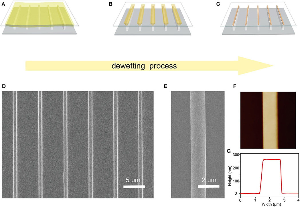
High-quality Cs2AgBiBr6 single-crystal microwire arrays were prepared through a capillary-bridge-mediated assembly method. The fabrication process of Cs2AgBiBr6 microwire arrays is schematically shown in Figures 1A–C. A sandwich-liked system, including a flat substrate (such as Si and glass), a periodic line-shape micropillar-structured template with superhydrophilic tops and hydrophobic sidewalls, and a drop of Cs2AgBiBr6 solution, is introduced to guide the dewetting process to yield pure orientated and high crystalline microwires. The micropillar-structured template was characterized by SEM (Supplementary Figure 1). The hydrophobic state of the sidewalls was realized by selectively modifying the FAS molecules. The schematic illustration FAS modification and wettability characterization are illustrated in Supplementary Figures 2, 3. The CA of the top is nearly 0°, showing a superhydrophilic state. The CA of the sidewall modified with FAS is about 120 ± 2°, demonstrating a hydrophobic state. A droplet of double-perovskite precursor was injected onto the asymmetric wettability template and then covered with a flat substrate to fabricate the Cs2AgBiBr6 microwire arrays. An entire liquid film was firstly formed between top surfaces of micropillars and the flat substrate because of the high adhesion of superhydrophilic tops. The gaps of the sidewalls were full of air, and no solution existed in those gaps. With the evaporation of the solvent, the continuous liquid film was separated into discrete line-shape capillary bridges pinned between superhydrophilic tops of the template and the substrate. Capillary bridges generated during the dewetting process could control the nucleation positions and direct the growth direction of the aimed high-quality microwire array. Capillary bridges shrunk and the concentrate of Cs2AgBiBr6 solution increased with the dewetting process going on. Once the solution saturated in capillary bridges, Cs2AgBiBr6 crystals would nucleate and constantly grow at the site pinned between micropillar tops and the target substrate. Finally, when the evaporation of the solvents completed, strict-aligned arrays were fabricated onto the target substrate.

Figure 1. Fabrication process and morphology characterization of Cs2AgBiBr6 microwire arrays. (A–C) Schematic illustration of the dewetting and crystallization process confined in capillary bridges. (D) SEM image of as-prepared Cs2AgBiBr6 microwire arrays. (E) Zoom-in SEM image of a single Cs2AgBiBr6 microwire. (F) AFM image of a single Cs2AgBiBr6 microwire showing its smooth surface and (G) its width and height.
Scanning electron microscopy (SEM) and atomic force microscopy (AFM) were carried out to characterize the crystallinity and surface morphology of the Cs2AgBiBr6 microwires. As Figure 1D shows, Cs2AgBiBr6 microwires have regular alignment and precise position. The zoom-in SEM image (Figure 1E) illustrates the microwire has a smooth surface and no visible grain boundary, indicating the high crystalline nature of these microwires. The AFM image (Figure 1F) shows an individual microwire with a smooth surface, a width of 1.5 μm, and a height of 260 nm (Figure 1G), which further demonstrates the high crystallinity of the microwire.
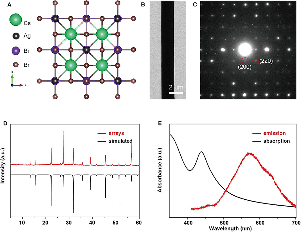
The transmission electron microscope (TEM), SAED, and XRD measurements are performed to investigate the crystal structure and crystallographic orientation of as-prepared Cs2AgBiBr6 arrays. We failed to record the high-resolution transmission electron microscope image (HRTEM) because of the easy decomposition of Cs2AgBiBr6 under strong electron beam radiation. UV-vis absorbance and photoluminescence (PL) spectra were performed at room temperature. The crystal structure of Cs2AgBiBr6 is depicted in Figure 2A (Yang et al., 2019). The TEM image (Figure 2B) illustrated that the microwire has a homogeneous surface and perfect morphology. The SAED pattern (Figure 2C) shows clear diffraction spots, demonstrating the good single crystal nature and the pure crystallographic orientation along [001]. As Figure 2D shows, the XRD pattern with sharp peak confirms the pure phase of Cs2AgBiBr6 (a = b = c = 11.27Å, α = β = γ = 90°, space group Fm-3m) without any other impurity, matching well with the results of the simulation. The absorption peak of the microwire arrays is at 438 nm, and the emission peak is at 570 nm (Figure 2E), which is consistent with a previous report (Pan et al., 2017).

Figure 2. Crystallographic and spectroscopic characterizations of single-crystalline, double-perovskite microwire arrays. (A) Crystal structure of Cs2AgBiBr6 single crystal viewed from [001] directions. (B) TEM image and (C) SAED pattern of a Cs2AgBiBr6 single-crystal microwire. (D) XRD pattern of Cs2AgBiBr6 microwire arrays compared with the corresponding simulation. (E) UV-vis absorption and PL emission spectra of Cs2AgBiBr6 microwire arrays.
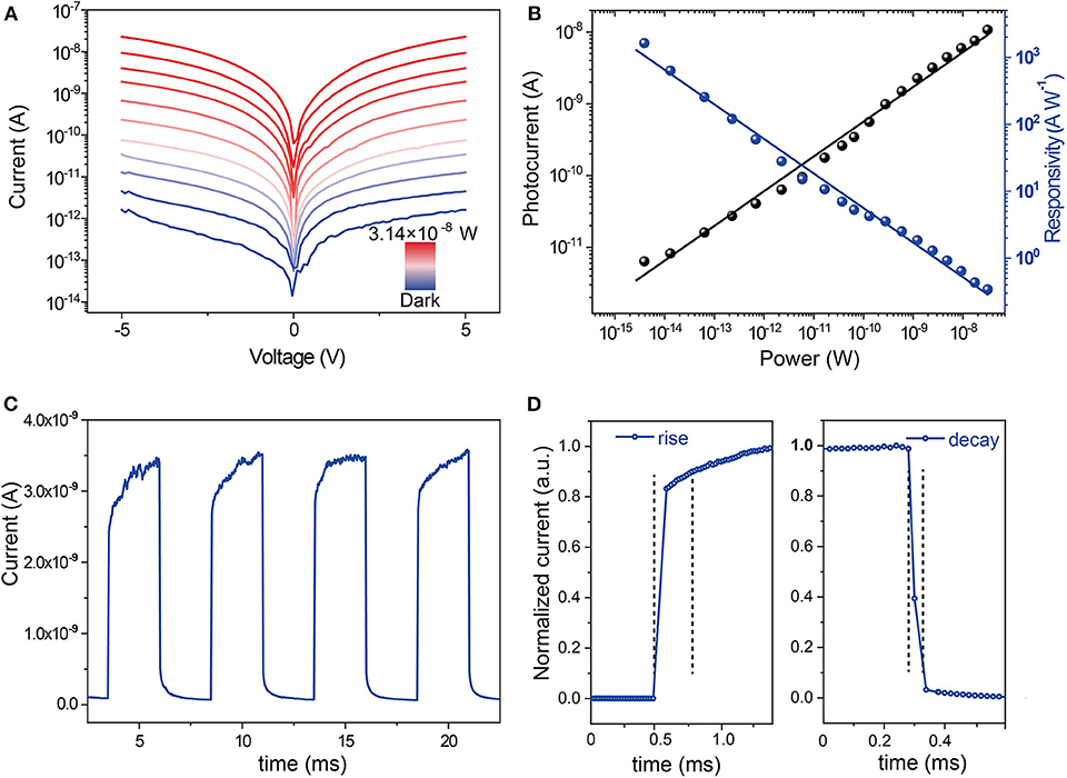
Then we investigated the performance of the fabricated detectors based on Cs2AgBiBr6 microwire arrays. The Cs2AgBiBr6 microwires were fabricated on SiO2/Si substrate, and Cr/Au (10/100 nm) electrodes were evaporated with shadow masks. The morphology of the device was characterized by SEM. A typical SEM image exhibits the structure of a photodetector based on several parallel Cs2AgBiBr6 microwires (Supplementary Figure 4). A series of I–V characteristic curves of Cs2AgBiBr6 arrays are displayed in Figure 3A, which were measured under dark conditions and 455 nm light illumination with different irradiation power by scanning bias from −5 to 5 V. The photodetector exhibits a current of 1.5 × 10⁻⁸ A with an irradiation intensity of 3.14 × 10⁻⁸ W and a dark current of 6.02 pA under the bias of 5 V, and thus, a light on–off ratio of 104 is calculated. The photocurrent increased with increasing irradiation power intensity, which was measured by Iph = Ilight–Idark, where Ilight and Idark are currents under light illumination and dark, respectively. The responsivity (R) of the detector was calculated by R = Iph/P, in which P is the incident light power. The responsivity reached 1,625 A W−1 under the irradiation intensity of 3.92 × 10⁻¹⁵ W. As Figure 3B shows, the photocurrent manifests a positive linear relationship with the illumination power, while the responsivity exhibits a negative linear relationship with the illumination power. The temporal photoresponse of the device was measured by periodically switching the light source with an intensity of 3.14 × 10⁻⁸ W, which is presented in Figure 3C, which suggests that the device has an excellent response toward the light state between on and off. The response time is defined as the current increase from 10 to 90% of the maximum for rise, and vice versa for decay. As shown in Figure 3D, the rise time is 0.28 ms and the decay time is 0.04 ms, indicating a fast response speed. The microwire with suppressed grain boundaries and high crystallinity is beneficial to the realization of high-performance optoelectronic devices. To verify the advantage of Cs2AgBiBr6 microwire arrays, we performed I–V measurements of the device based on the spin-coated polycrystalline thin film. The SEM image of the thin film was displayed in Supplementary Figure 5. The current of the thin film with the irradiation intensity of 3.14 × 10⁻⁸ W and under the bias of 5 V is 3.1 × 10⁻¹⁰ A (Supplementary Figure 6), which is less than that of microwire arrays, while the dark current of the film is a little higher than that of microwire arrays. The responsivity of the photodetector based on the Cs2AgBiBr6 thin film was only 0.68 A W−1, which is three orders of magnitude lower than that of Cs2AgBiBr6 microwire arrays. The high-efficiency photocarrier generation attribute to the high crystalline nature and suppressed grain boundaries of Cs2AgBiBr6 microwire arrays, thus leading to higher performance of photodetectors based on microwire arrays.

Figure 3. Performances of the photodetector based on single-crystalline Cs2AgBiBr6 microwire arrays. (A) I-V curves of the device under different illumination intensities and dark conditions. (B) The photocurrent and responsivity of the device under different illumination power. (C) I–t response with four on-off cycles and (D) temporal response of the device.
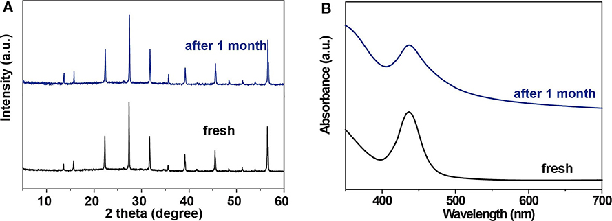
It has been demonstrated that the bulk Cs2AgBiBr6 single crystal has good resistance to heat treatment and humid atmosphere (Ning et al., 2019). Our microwires are expected to have good stability too. To assess the stability of Cs2AgBiBr6 microwire arrays, we fabricated microwire arrays on a Si substrate and kept it under ambient conditions for 30 days. We measured XRD and absorption spectra to verify their stability. As shown in Figures 4A,B, the XRD pattern and absorption curve keep consistent with initial characterizations, suggesting that Cs2AgBiBr6 microwire arrays have excellent stability in ambient conditions.

Figure 4. Stability of single-crystalline Cs2AgBiBr6 microwire arrays. (A) XRD patterns and (B) absorption spectra of Cs2AgBiBr6 microwire arrays before and after the storage at room temperature (22°C) and relative humidity of 30% in air conditioning, respectively.
Conclusion
We employ the capillary-bridge-assisted method to prepare Cs2AgBiBr6 microwire arrays with a smooth surface, pure orientation, and ordered alignment, then demonstrating non-toxic blue-light photodetectors with high performance and long-term stability. Capillary bridges control the fluid dynamics in the dewetting process, thus leading to the oriented growth of Cs2AgBiBr6 microwire arrays. Compared to the Cs2AgBiBr6 polycrystalline film with a large grain boundary, as-prepared microwire arrays have large grain sizes and eliminated grain boundaries, which are beneficial for improving the performance of devices. Photodetectors based on double-perovskite microwire arrays exhibit a high responsivity of 1,625 A W−1, on-off ratio exceeding 104, and fast response speed. We believe that our work provides a new alternative for the integration of non-toxic perovskite photodetectors based on perovskite single-crystal arrays.
Data Availability Statement
The raw data supporting the conclusions of this article will be made available by the authors, without undue reservation.
Author Contributions
YP, JZ, and YZ contributed equally to this manuscript. YP, JZ, and HG co-wrote the manuscript. YZ performed the experiments. JF, HG, YW, and LJ designed the project. HG, CZ, YW, and LJ discussed the results part and revised the manuscript. All authors approved the final version of the manuscript.
Funding
The authors acknowledge MOST of China (Grant Nos. 2018YFA0704803, 2017YFA0204504, and 2018YFA0208502), National Natural Science Foundation (51922012, 21703268, and 21633014), Beijing Municipal Science & Technology (Z181100004418014), and Beijing Natural Science Foundation (2182081).
Conflict of Interest
The authors declare that the research was conducted in the absence of any commercial or financial relationships that could be construed as a potential conflict of interest.
The reviewer QY declared a shared affiliation, though no other collaboration, with the authors YP, CZ to the handling editor.
Supplementary Material
The Supplementary Material for this article can be found online at: https://www.frontiersin.org/articles/10.3389/fchem.2020.00632/full#supplementary-material
References
Ahmadi, M., Wu, T., and Hu, B. (2017). A review on organic-inorganic halide perovskite photodetectors: device engineering and fundamental physics. Adv. Mater. 29:1605242. doi: 10.1002/adma.201605242
Chen, G. S., Feng, J. G., Gao, H. F., Zhao, Y. J., Pi, Y. Y., Jiang, X. Y., et al. (2019). Stable α-CsPbI3 perovskite nanowire arrays with preferential crystallographic orientation for highly sensitive photodetectors. Adv. Funct. Mater. 29:1808741. doi: 10.1002/adfm.201808741
Chen, G. S., Qiu, Y. C., Gao, H. F., Zhao, Y. J., Feng, J. G., Jiang, L., et al. (2020). Air-stable highly crystalline formamidinium perovskite 1D structures for ultrasensitive photodetectors. Adv. Funct. Mater. 29:1908894. doi: 10.1002/adfm.201908894
Chen, Z., Dong, Q., Liu, Y., Bao, C., Fang, Y., Lin, Y., et al. (2017). Thin single crystal perovskite solar cells to harvest below-bandgap light absorption. Nat. Commun. 8:1890. doi: 10.1038/s41467-017-02039-5
Chen, Z., Li, C., Zhumekenov, A. A., Zheng, X., Yang, C., Yang, H., et al. (2019a). Solution-processed visible-blind ultraviolet photodetectors with nanosecond response time and high detectivity. Adv. Optical Mater. 7:1900506. doi: 10.1002/adom.201900506
Chen, Z., Turedi, B., Alsalloum, A. Y., Yang, C., Zheng, X., Gereige, I., et al. (2019b). Single-crystal MAPbI3 perovskite solar cells exceeding 21% power conversion efficiency. ACS Energy Lett. 4, 1258–1259. doi: 10.1021/acsenergylett.9b00847
Chu, L., Ahmad, W., Liu, W., Yang, J., Zhang, R., Sun, Y., et al. (2019). A new superstar toward green and stable optoelectronic applications. Nano Micro Lett. 11:16. doi: 10.1007/s40820-019-0244-6
Dai, C. M., Zhang, T., Wu, Y. N., and Chen, S. Y. (2020). Halide double-perovskite light-emitting centers embedded in lattice-matched and coherent crystalline matrix. Adv. Func. Mater. 30:2000653. doi: 10.1002/adfm.202000653
Gao, H. F., Feng, J. G., Pi, Y. Y., Zhou, Z. H., Zhang, B., Wu, Y. C., et al. (2018). Bandgap engineering of single-crystalline perovskite arrays for high-performance photodetectors. Adv. Funct. Mater. 28:1804349. doi: 10.1002/adfm.201804349
Greul, E., Petrus, M. L., Binek, A., Docampo, P., and Bein, T. (2017). Highly stable, phase pure Cs2AgBiBr6 double perovskite thin films for optoelectronic applications. J. Mater. Chem. A 5, 19972–81. doi: 10.1039/C7TA06816F
Igbari, F., Wang, Z. K., and Liao, L. S. (2019). Progress of lead-free halide double perovskites. Adv. Energy. Mater. 9:1803150. doi: 10.1002/aenm.201803150
Li, Z. Z., Xu, Q. C., Sun, Q. D., Hou, Z. F., and Yin, W. J. (2019). Thermodynamic stability landscape of halide double perovskites via high-throughput computing and machine learning. Adv. Funct. Mater. 29:1807280. doi: 10.1002/adfm.201807280
Muhammad, U., and Yan, Q. F. (2020). Recent advancements in crystalline Pb-free halide double perovskites. Crystals 10:62. doi: 10.3390/cryst10020062
Ning, W. H., and Gao, F. (2019). Structural and functional diversity in lead-free halide perovskite materials. Adv. Mater. 31:1900326. doi: 10.1002/adma.201900326
Ning, W. H., Wang, F., Wu, B., Lu, J., Yan, Z. B., Liu, X. J., et al. (2018). Long electron-hole diffusion length in high-quality lead-free double perovskite films. Adv. Mater. 30:1706246. doi: 10.1002/adma.201706246
Ning, W. H., Zhao, X. G., Klarbring, J., Bai, S., Ji, F. X., Wang, F., et al. (2019). Thermochromic lead-free halide double perovskites. Adv. Funct. Mater. 29:1807375. doi: 10.1002/adfm.201807375
Pan, W. C., Wu, H. D., Luo, J. J., Deng, Z. Z., Ge, C., Chen, C., et al. (2017). Cs2AgBiBr6 single-crystal X-ray detectors with a low detection limit. Nat. Photon. 11, 726–732. doi: 10.1038/s41566-017-0012-4
Schade, L., Wright, A. D., Johnson, R. D., Dollmann, M., Wenger, B., Nayak, P. K., et al. (2018). Structural and optical properties of Cs2AgBiBr6 double perovskite. ACS. Energy. Lett. 4, 299–305. doi: 10.1021/acsenergylett.8b02090
Slavney, A. H., Hu, T., Lindenberg, A. M., and Karunadasa, H. I. (2016). A bismuth-halide double perovskite with long carrier recombination lifetime for photovoltaic applications. J. Am. Chem. Soc. 138, 2138–2141. doi: 10.1021/jacs.5b13294
Steele, J. A., Pan, W. C., Martin, C., Keshavarz, M., Debroye, E., Yuan, H., et al. (2018). Photophysical pathways in highly sensitive Cs2AgBiBr6 double-perovskite single-crystal X-Ray detectors. Adv. Mater. 30:1804450. doi: 10.1002/adma.201804450
Weng, Z. H., Qin, J. J., Akrajas, A. U., Wang, J., Zhang, X., Wang, H. L., et al. (2019). Lead-free Cs2AgBiBr6 double perovskite-based humidity sensor with superfast recovery time. Adv. Funct. Mater. 29:1902234. doi: 10.1002/adfm.201902234
Wu, C. C., Zhang, Q. H., Liu, Y., Luo, W., Guo, X., Huang, Z. R., et al. (2018). The dawn of lead-free perovskite solar cell: highly stable double perovskite Cs2AgBiBr6 film. Adv. Sci. 5:1700759. doi: 10.1002/advs.201700759
Yang, B., Pan, W. C., Wu, H. D., Niu, G. D., Yuan, J. H., Xue, K. H., et al. (2019). Heteroepitaxial passivation of Cs2AgBiBr6 wafers with suppressed ionic migration for X-ray imaging. Nat. Commun. 10:1989. doi: 10.1038/s41467-019-09968-3
Keywords: double perovskite, microwire array, photodetector, non-toxic, stable
Citation: Pi Y, Zhao J, Zhao Y, Feng J, Zhang C, Gao H, Wu Y and Jiang L (2020) Capillary-Bridge Controlled Patterning of Stable Double-Perovskite Microwire Arrays for Non-toxic Photodetectors. Front. Chem. 8:632. doi: 10.3389/fchem.2020.00632
Received: 01 May 2020; Accepted: 17 June 2020;
Published: 25 August 2020.
Edited by:
Zhaolai Chen, Shandong University, ChinaCopyright © 2020 Pi, Zhao, Zhao, Feng, Zhang, Gao, Wu and Jiang. This is an open-access article distributed under the terms of the Creative Commons Attribution License (CC BY). The use, distribution or reproduction in other forums is permitted, provided the original author(s) and the copyright owner(s) are credited and that the original publication in this journal is cited, in accordance with accepted academic practice. No use, distribution or reproduction is permitted which does not comply with these terms.
*Correspondence: Chi Zhang, Y2hpemhhbmdAbWFpbC50c2luZ2h1YS5lZHUuY24=; Hanfei Gao, Z2FvaGFuZmVpMTVAbWFpbHMudWNhcy5hYy5jbg==
 Yueyang Pi1
 Yuchen Wu