 Rosaria Anna Picca1,2*
 Kyriaki Manoli1,2Eleonora Macchia1,3
 Angelo Tricase1
 Cinzia Di Franco4
 Gaetano Scamarcio2,4,5Nicola Cioffi1,2
 Luisa Torsi1,2,3*
- 1Dipartimento di Chimica, Università degli Studi di Bari “Aldo Moro”, Bari, Italy
- 2Consorzio per lo Sviluppo dei Sistemi a Grande Interfase, Unità di Bari, Bari, Italy
- 3The Faculty of Science and Engineering, Center for Functional Materials, Åbo Akademi University, Turku, Finland
- 4CNR - Istituto di Fotonica e Nanotecnologie, Unità di Bari, Bari, Italy
- 5Dipartimento Interateneo di Fisica “M. Merlin”, Università degli Studi di Bari “Aldo Moro”, Bari, Italy
Robust electrolyte-gated organic field-effect-transistors (OFETs) are particularly needed for the development of biosensing devices. However, when a FET biosensor operates in aqueous environments or even in real biological fluids, some critical issues may arise due to the possible lack of environmental long-term and/or operational stability. An important source of instability is associated with the degradation of the organic electronic channel materials such as for instance, poly-3-hexylthiophene (P3HT), a benchmark commercially available p-type organic semiconductor. In this work, the investigation of critical parameters, such as the control over spurious electrochemical phenomena as well as the operating conditions that can affect water-gated OFETs lifetime, is reported, together with a proposed modeling of the P3HT stability curve over 1 week in water. The investigation of possible morphological/chemical modifications occurring at the polymer surface after operating in water for 2 weeks was carried out. Moreover, it is proven how the addition of a gel layer can extend the P3HT based water-gated OFET shelf life up to 2 months.
Introduction
The use of organic field-effect-transistors (OFETs) as sensors (Torsi et al., 2013; Li et al., 2018; Surya et al., 2019) has received a tremendous boost in the last decades thanks to the advent of low-cost fabrication strategies as well as of flexible and/or stretchable substrates (Kim et al., 2013; Manoli et al., 2015). However, their exploitation and commercialization as real-life sensors have been limited by the organic polymer degradation occurring when the device is operated in aqueous environments (Knopfmacher et al., 2014; Wang et al., 2016; Zhang et al., 2016). Extensive literature on the operational and environmental stability of organic semiconductors have been reported for devices working with solid-state dielectrics (Salleo et al., 2005; Sirringhaus, 2009; Bobbert et al., 2012; Nikolka et al., 2016; Lee et al., 2017; Jia et al., 2018) addressing the role of external agents (e.g., water, oxygen, light) in reducing the device performance. Evidences of device degradation encompass the increased hysteresis on transfer curves and leakage (IG) for successive measurements, threshold voltage (VT) shift, on current (Ion) decrease with time (Sirringhaus, 2009). Such behavior has been mainly ascribed to the uncompensated charged trapped in deep localized states in the semiconductor also caused by spurious electrochemical processes (Sirringhaus, 2005; Beatrup et al., 2014; Porrazzo et al., 2014). For example, the presence of polaronic states can cause an increased susceptibility to the electrochemical degradation (Wade et al., 2015). In fact, the presence of hole polarons under device operation is found to make polaron degradation pathways accessible (Beatrup et al., 2014). Moreover, a charge transfer complex may be formed with oxygen (favored under light) leading to instability (Bellani et al., 2014).
Some alternatives to overcome such drawbacks have been proposed, such as the inclusion of ZnO nanophases in the bioreceptor layer of OFET biosensors (Picca et al., 2018) or polymer encapsulation (Yu et al., 2016; Lee et al., 2017). More recently, electrolyte-gated devices (EGOFETs) have emerged as interesting devices that can operate in the sub-volt regime (Panzer and Frisbie, 2008; Kergoat et al., 2010; Cramer et al., 2013) thus paving the way to their application in label-free ultra-sensitive biosensors (Mulla et al., 2015; Macchia et al., 2018a,b, 2019a,b).
In EGOFETs, two electrical-charge-double-layers (EDL) are built: one at the gate/electrolyte and the other at the electrolyte/organic semiconductor interfaces. When water serves as electrolyte, the EDL capacitance is remarkably high, being in the order of few μF*cm−2 (Cramer et al., 2013). In such an architecture, the direct contact between the organic semiconductor (OS) layer and the aqueous environment rises concerns about the already investigated degradation induced in such polymers by electrochemical processes that occur in water (de Leeuw et al., 1997; Sharma et al., 2010; Bobbert et al., 2012), that are particularly detrimental leading to unstable EGOFETs on prolonged use (Cramer et al., 2013; Bellani et al., 2014; Porrazzo et al., 2014). Until now, only few studies about EGOFET devices have addressed this issue reporting on stability over time (Zhang et al., 2016) or under harsh environments (Porrazzo et al., 2014; Algarni et al., 2016). In this work, poly-3-hexylthiophene (P3HT) was chosen as benchmark p-type OS used to fabricate water-gated OFETs, employing a bulk gold foil as gate electrode. At first, the reduction of hysteretic behavior was demonstrated by setting up a suitable measuring protocol. Moreover, environmental (incubation in HPLC water) and operational stability (cycling mode) studies were carried out demonstrating the main role of the electrolyte over the measuring conditions in device degradation. A suitable cell was also designed to overcome the problem of water evaporation during measurements. Interestingly, P3HT degradation was modeled in terms of ID decrease with a two-phase exponential decay function indicating that a first process occurs within few hours, whereas a second one has a time constant in the order of 35 h. It was demonstrated that a similar trend is mainly associated to VT negative shift with time. A strategy to extend EGOFET use over the months was also investigated. Additional morphological and spectroscopic characterizations performed on as-prepared and used devices provided information about the response of P3HT film to water contact on a long time scale (2 weeks).
Materials and Methods
Fabrication of EGOFET Devices
Highly n-doped silicon substrates, covered by 300-nm thermally grown SiO2, were purchased from Si-Mat®. Source (S) and drain (D) interdigitated electrodes were photo-lithographically patterned on the Si/SiO2 wafer. To this end, a Ti (99.995%) film (5 nm thick) was deposited as adhesion layer prior of the Au (99.99%) film (50 nm thick) deposition by electron-beam evaporation. The S&D interdigitated electrodes have a channel length (L) of 5 μm and a channel width (W) of 10,560 μm. Poly(3-hexylthiophene-2,5-diyl) (regioregular, electronic grade, 99.995% trace metal basis, average Mn ~17,500, Sigma-Aldrich), P3HT, was used as p-type OS throughout the study. The polymer was first dissolved in chlorobenzene (2.6 mg/mL), and then the solution was sonicated for 20 min prior to filtration through a PTFE 0.2 μm syringe filter. Before depositing the OS film, substrates bearing the interdigitated electrodes were cleaned under ultrasounds in an acetone bath (10′) followed by a similar step in 2-propanol and finally dried under nitrogen. P3HT film was spin coated at 2,000 rpm for 20 s and annealed at 90°C for 10 min. A channel area of 6.4·10−3 cm2 was estimated (Macchia et al., 2018a). The gate electrode (G) consisted of an Au bulk sheet (total area ~1.5 cm2) mounted in L-configuration, whose water immersed area was about 0.6 cm2. When specified, a channel consisting of P3HT/ZnO nanoparticles hybrid layer was prepared by spin coating starting from a filtered P3HT solution mixed with ZnO nanoparticles (Picca et al., 2015) (1.5 mg/mL final concentration).
A suitable well for performing long-term studies under water was designed and fabricated to prevent possible water evaporation. It consists of a polystyrene (PS) cell glued with polydimethylsiloxane on the substrate. A PTFE tube connects the cell to a proper water reservoir in order to keep the water level constant in the well. The well is filled with 1.2 mL of water (HPLC-grade, Honeywell Riedel-de Haën) acting as gating medium. The scheme and the picture of the measuring set up are presented in Figure 1.
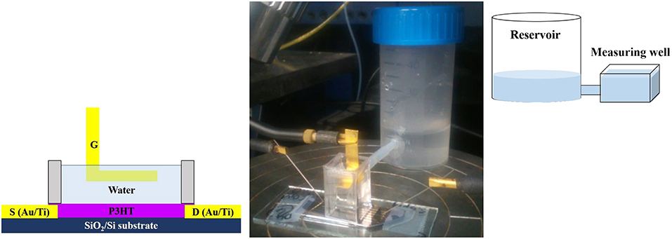
Figure 1. Scheme and picture of the set up used for studying EGOFET devices. A top-gate bottom-contacts configuration is adopted.
EGOFET Electrical Characterization
All the devices were characterized by means of a Keithley 4200-SCS semiconductor characterization system in air at room temperature (20–22°C) in a dark box. The drain current (ID) was acquired scanning the gate voltage (VG) between 0.1 and −0.5 V, keeping the drain voltage (VD) at −0.4 V. The voltage step was set at 0.01 V. The source is grounded as typical in common source configuration measurements. Forward and backward scans were performed to evidence the occurrence of hysteretic behavior. A suitable measuring protocol was also set up as described in the results section. The potential window was defined according to the need to prevent any electrochemical process to occur and affect the EGOFET. To this aim, gate current (IG) was also registered in order to monitor any spurious electrochemical process. Electrical figures-of-merit (μFET and VT) were extracted from the ID-VG transfer characteristics in the saturation regime according to a well-known procedure (Torsi and Dodabalapur, 2005) and are averaged on 10 different devices (n = 10) operated in independent measurements. Error bars refer to one standard deviation calculated considering n = 10.
Morphological Analysis
Scanning electron microscopy (SEM) was applied to investigate the in-plane homogeneity of OS films deposited by spin coating. Analysis was performed by means of a Carl Zeiss Σigma field emission SEM on films prepared, both on interdigitated electrodes and on SiO2/Si substrates. The probing electron beam was set at an acceleration voltage of 3–5 kV acquiring images at different magnifications in top-view. SE2 type detector was used to acquire the overall image of the device (Figures 2A,C), whereas the detailed view of the samples was recorded with the in-lens detector (Figures 2B,D).
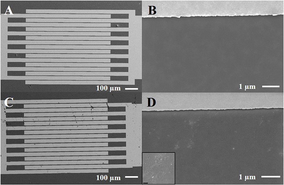
Figure 2. Scanning electron micrographs of P3HT film deposited onto interdigitated electrodes, before (A,B) and after 2 weeks under water (C,D). The inset refers to a zoom at higher magnification (scale bar corresponds to 200 nm) of the exposed sample.
Atomic Force Microscopy (AFM) characterization was performed on P3HT-based EGOFETs, just after their preparation and after contact with water for 2 weeks. AFM images were collected with a NT-MDT mod. Ntegra microscope in semi-contact mode using a tip apex size of 10 nm at a frequency f = 180 kHz. For each sample, areas of 3 × 2 μm were investigated. The Image Analysis Software was used to evaluate the surface roughness as route mean squared (RMS) on at least three representative areas of the sample.
X-ray Photoelectron Spectroscopy Surface Analysis
P3HT-based FETs were analyzed by means of X-ray photoelectron spectroscopy (XPS) using a PHI Versaprobe II Spectrometer. A monochromatized Al Kα radiation (1486.6 eV) was used. Survey spectra were acquired with a pass energy of 117.4 eV; whereas high-resolution (HR) spectra were acquired with a pass energy of 58.7 eV. C1s, O1s, Si2p, S2p, Au4f regions were investigated. Both as-prepared and used samples were characterized. MultiPak™ (v. 9.7.0.1, PHI-ULVAC) software was used to process the data. Binding energy (BE) scale was corrected taking as reference C1s component at 284.8 eV. Three representative areas of the sample were collected to evaluate the chemical surface composition.
Results and Discussion
SEM Characterization of P3HT Films
P3HT organic semiconductor has been typically successfully used by our group as active channel in FET biosensors with different architectures (Angione et al., 2012; Magliulo et al., 2013; Macchia et al., 2016). As a general procedure, P3HT films were prepared by spin-coating starting from a chloroform solution. However, SEM investigation on similar samples showed that P3HT layers were not uniform due to the presence of some voids and agglomerates (Sportelli et al., 2017). Chlorobenzene was then selected because of its higher boiling point as alternative solvent to improve layer uniformity and crystallinity, in agreement with what previously reported in the literature (Kergoat et al., 2011). SEM images of typical P3HT films, freshly deposited on a plain SiO2/Si substrate and on gold electrodes, are presented in Figures 2A,B. It is evident that a rather uniform OS layer is formed confirming the advantages of processing P3HT from chlorobenzene. The very same samples were put in contact with water for 2 weeks and used as EGOFET devices (vide infra) and then characterized by SEM to evaluate a possible modification of layer uniformity. Additional features appear in the images (Figures 2C,D), though it seems that they are mainly related to the effect of water evaporation and presence of dust/salt particles (see the inset of the Figure). In fact, cracks and/or delamination of the polymer are not evident.
AFM Characterization of the OS Layer
Figure 3 shows two typical AFM images of an area of a P3HT FET, before (a) and after (b) 2-week exposure to water. RMS was calculated as an estimate of the roughness in both cases. A general increase in the roughness going from 0.5 ± 0.1 nm for pristine samples to 1.6 ± 0.2 nm after use was found. The low roughness observed on freshly prepared films is indicative of the goodness of the solvent using for processing the polymer in agreement with SEM results. After 2-week contact with water, the RMS increment can be attributed to a sort of polymer swelling. Nonetheless, dramatic changes in the surface morphology are not visible which account for the preservation of the FET modulation, at least in the investigated time scale.
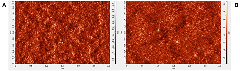
Figure 3. AFM images of P3HT film deposited onto interdigitated electrodes, before (A) and after 2 weeks under water (B).
XPS Characterization of P3HT Active Layers
The surface chemical composition of fresh and used P3HT-based devices was determined by XPS analysis (Table 1). The chemical composition does not seem particularly affected by contact with water, apart the higher oxygen content. Such finding is confirmed by spectral comparison of C1s, O1s, S2p regions (Figure 4) acquired before and after long exposure to water. Slight increment in carbon oxygenated components is observed (BE > 286 eV) suggesting a certain chemical degradation of the polymer. Nonetheless, the lineshape of S2p signal is preserved suggesting no oxidation on Sulfur. Interestingly, increment in the oxygen content is correlated to the presence of hydroxyl groups in addition to the O1s component ascribed to SiO2 (BE = 532.5 ± 0.2 eV) (National Institute of Standards and Technology, 2012). XPS results suggest then that a partial modification of the polymer occurs within the investigated period, accounting for the increased roughness and the reduced electrical performance upon long exposure to water.
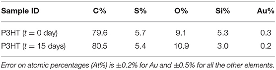
Table 1. Typical surface chemical composition of fresh (t = 0) and aged (t = 15 days in water) P3HT samples.
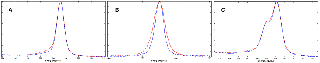
Figure 4. C1s (A), O1s (B), S2p (C) XP regions registered for P3HT-based FETs, before (blue curves) and after contact with water for 2 weeks (red curves).
The Measuring Protocol
As anticipated, hysteresis, i.e., the difference between ID values measured in the forward and backward gate voltage sweep, is one of the main issues that can arise when OFET devices are operated. In these cases, this behavior has been often attributed to the presence of moisture in the OS layer or at the OS/dielectric interface, especially when SiO2 is used as gate dielectric (Bobbert et al., 2012). On the other hand, water-gated OFETs show minor hysteresis phenomena. This is mainly attributed to the absence of proton trapping in a dielectric and the occurrence of their neutralization by water autoprotolysis (Cramer et al., 2013). Hysteresis can be influenced by the sweeping potential window and by the scan rate of the applied potential (Panzer et al., 2005). For example, it was shown that scanning the VG from the off to the on state (and vice versa) by applying pulses of alternating polarities was a suitable method to get hysteresis-free transfer curves in P3HT based FETs (Manoli et al., 2014). In this work, a similar protocol was adopted as reported in the Supplementary Material. It was observed that, regarding VG sweep protocol, keeping the on time equal to 10 ms (+1 s cumulative measure time) as compared to the off time (1 s) and selecting −0.05 V as base voltage, gave the best results. This means that a slow scan rate of about 40 mV/s is applied to VG. Moreover, the VD set at a maximum value of −0.4 V, was also pulsed keeping the on time (1 s) longer than the off time (0.1 s) at 0 V. A comparison between the performances of water-gated P3HT FETs operated in the DC-mode (red curves) or in the pulse-mode (black curves) is presented in Figure 5. The drain and the leakage currents (IG) are reported as a function of VG for the two cases. Apparently, the pulse mode contributes to measure a slightly increase ID, and more relevantly to measure an almost hysteresis-free and reduced gate leakage current level. Taking the current values at VG = −0.5 V, the ratio ID/IG in the pulse-mode was about twice the one measured in the DC-mode.
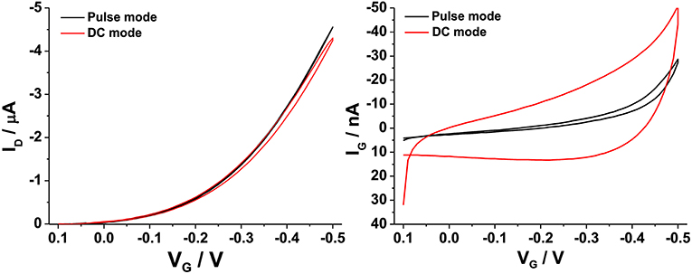
Figure 5. ID-VG (left) and IG-VG (right) curves registered on a P3HT water-gated FET in pulse (black curves) or continuous (red curves) mode.
Operational Stability
The definition of a proper measurements protocol was beneficial to improve EGOFET performance level; however, it was not sufficient in limiting the degradation phenomena and hence the device long-term stability and reliability. In this respect, it is worth to dwell into the operational stability as well. A general scheme reported in literature involves the use of the so-called bias-stress mode consisting in the application of a continuous gate bias over time (Sirringhaus, 2009), though other approaches based on the cycling measurements of transfer curves have also been applied (Hwang et al., 2011). In this work, the interest was focused on the aspects connected with the application of EGOFETs as biosensing platforms; therefore, the operational stability of P3HT based devices was studied in water. To this aim, the typical sensing protocol followed in our laboratory in single-molecule detection (Macchia et al., 2018a) was simulated and the transfer curves of the fabricated devices were measured every half an hour using water and Au sheet as gating medium and gate electrode, respectively. A 30 min interval was chosen to mimic the time generally passing between two successive exposures to analyte solutions in a conventional sensing experiment. In fact, it is fundamental to get highly stable devices before using them in sensing platforms (Macchia et al., 2019b). P3HT based devices were then tested just after their fabrication. An example of the variation of the maximum current, ID(max) (measured at VG = −0.5 V), over 48 h is shown in Figure 6A. It can be seen that a dramatic decrease in current occurs in the first cycles, whereas the current level almost reaches a steady state after 24 h. This trend was not surprising considering that the devices are not operated in an inert atmosphere. An alternative approach was explored to discriminate both the role of the measuring environment and of the operational protocol. Some devices were kept in contact with water just after their preparation (pristine sample) without operating them for the first 18 h. In this case, ID(max) variation over time (blue hollow triangles) is presented in Figure 6B. Interestingly, the two experiments led to very similar results, thus suggesting that the pronounced initial ID decrease is essentially correlated to the adjustment of the polymer film in water environment. Quantitatively, a current decay of about 35% was generally observed for both the 18 h-cycled or the 18 h-water-incubated samples as reported in Figure 7. This fundamental aspect has never been clearly addressed in previous works about operational stability of OFET devices in water. It is worth noting that a similar decay was also reported for devices based on OS blended with polystyrene after 11 h of operation in water. In this case, a current decrease rate of about 3%/h was reported (Zhang et al., 2016). In this work, we observed that devices comprising a commercial P3HT seem more stable even in the first day after their preparation. After this period, the current drift is typically reduced and is around 1%/h allowing the P3HT based device to be very well suited to be used in ultra-sensitive biosensing experiments (Macchia et al., 2019b).
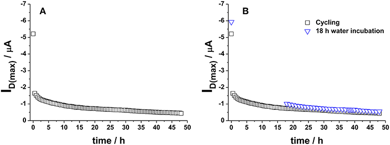
Figure 6. (A) ID(max) (measured at VG = −0.5 V) variation over 48 h when cycling mode is applied to water-gated P3HT FET. Data refer to transfer curves acquired every 30 min. (B) Comparison between ID(max) values reported in (A) and ID(max) registered on a water-gated P3HT FET incubated in water for 18 h (without operating it) (blue hollow triangles).
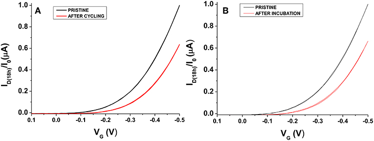
Figure 7. ID-VG curves taken before (black) and after (red) 18 h for water-gated P3HT FETs operated in cycle mode (A) or just put in contact in water (B). ID has been normalized on the initial ID value (I0).
The timescale of this characterization was further extended taking into account the variation of the electrical figures-of-merit, μFET, VT, and ID(max), over a time lease of 2 weeks. In this case, the devices were kept in water and measured in cycling mode for 5 h per day. The current values at t = 0 day and at t = 15 days are given in Table 2. The EGOFET devices comprising a P3HT channel material modified with an n-type nanostructured oxide were also tested under the same conditions. Such investigation was undertaken because in our previous studies ZnO nanoparticles were implemented in OFETs giving good performance in terms of electrical properties (Picca et al., 2015) and stability (Picca et al., 2018).
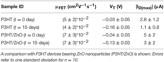
Table 2. Device figures of merit estimated on fresh and aged samples (used for 2 weeks).
At a first inspection, it can be observed that the device degradation translates into a negative shift of the threshold voltage, VT. Interestingly, mobility seems almost unaffected by the prolonged device operation in water. Similar findings were reported in other systems, as well. Moreover, the electrical performance and the stability of the devices were not significantly improved by the addiction of the ZnO nanostructures. This is not so surprising since in the previous work ZnO was deposited as separate layer underneath the P3HT film in a functional bio-interlayer OFET biosensor, thus behaving as capturing layer for water molecules at the interface between P3HT and the solid dielectric (Picca et al., 2018). On the other hand, recent data on water-gated devices based on P3HT films modified with WS2 nanotubes showed an increased operational stability, quite likely due to the nanoscale morphology of the active blend layer (Macchia et al., 2018c).
As expected, the degradation cannot be avoided but it is in the order of the one reported for EGOFETs based on other materials. In fact, the current level was reduced of about 30% of its original value after 7 days (Figure 8), in agreement with data available in literature (Zhang et al., 2016). Furthermore, the study was focused on the modeling of device degradation under the experimental conditions explored in this work. In the past, works related to devices operating with a solid-state dielectric under bias stress proved that the VT shift correlates with current decay, whereas mobility is almost unchanged (Salleo et al., 2005). Bias stress instability translates into a voltage threshold shift, and hence into ID decay, which can be generally modeled with a single exponential decay function (Zhang et al., 2009). In the paper by Salleo et al. (2005) it was also observed that on a very short timescale (<100 s) almost all the charged traps could be recovered after bias removal indicating that these defect states have a short lifetime and are probably located in the more ordered regions of the organic semiconductor. In the same work, a long-lived component of trapped charges was also invoked. These traps are characterized by slow kinetics as they can last for days, thus being responsible for the observed lower VT shift. It is believed that they are present in deep states, quite likely distributed in the disordered portions of P3HT.
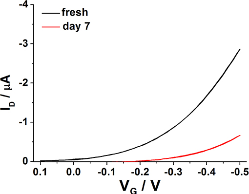
Figure 8. Typical transfer curves registered on a water-gated P3HT FET, just after fabrication (black line) and after 7 days (red line).
In the field of EGOFETs, little is known about device degradation under operation and empirical approaches are typically employed to describe their behavior, typically carrying out the studies on a limited period (hours). Based on the experimental conditions employed in this work, the degradation of the prepared devices was followed in terms of ID(max) decay and VT variation over 7 days (Figure 9). A double exponential decay function, expressed as y = A1*exp(–x/t1) + A2*exp(–x/t2) + y0, was used to fit both parameters. It is worth mentioning that such expression was already used in other works to describe recovery in pulse duty cycle studies (Miyadera et al., 2008; Manoli et al., 2014). However, both previous papers referred to OFET systems. The two extracted time constants (t1, t2) are similar for both drain current and threshold voltage changes, in agreement with previous observations. In particular, t1 is 1.8 ± 0.5 h and t2 is 35 ± 3 h. This means that two distinct processes impact on P3HT degradation processes occurring at different times. The first decay is responsible for the “rapid” current loss in the initial time-frame right after the incubation in water. Such trend could be in principle recovered within few days after stress removal (Sirringhaus, 2009). The second process may result from the presence of uncompensated immobile charges in the OS film. Obviously, due to continuous contact with the electrolyte, other effects such as the partial penetration of water in the P3HT film as well as formation of a passivating oxide layer on gold should be also taken into account. In particular, AFM and XPS results indicate that slight modifications in terms of morphology and composition of the polymer occur when devices are operated in water over a long period thus supporting the existence of degradation pathways responsible for the irreversible components of the decay model. It was generally reported that water molecules can penetrate the OS layer being then enclosed in the polymer nanovoids and causing trap formation (Nikolka et al., 2016; Zuo et al., 2019). This means that the latter component of degradation cannot be easily recovered and further studies will be necessary to clarify this behavior.
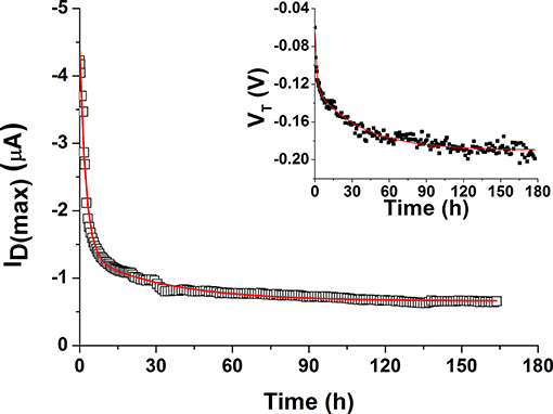
Figure 9. Modeling of P3HT degradation over 7 days, expressed as ID(max) vs. time. In the inset, the shift in the threshold voltage is also fitted with the same function.
Shelf Life Extension
An important aspect for the development of EGOFET biosensors is related to their storage as well as to the possibility to use them several times. When continuously operated in water, it was observed that the very maximum time frame in which P3HT based OFETs can be used is about 20 days as upper limit. A protocol for improving their durability was then applied. As a proof-of-concept, agarose gel was employed as protecting layer for the P3HT channel when the device was not in use. In the proposed set up, 1%w agarose (300 μL) solution was poured on the P3HT film and let jellify directly in the measuring well. Then, the devices could be stocked in the dark at ambient conditions. The important point is that the device was constantly kept in contact with the water trapped in the gel-matrix. When needed, the agarose film could be easily removed and substituted with water for further device electrical characterization. After use, the gel layer could be deposited again. Shelf life was evaluated in terms of ID measured on different days by acquiring a transfer curve, as reported in Figure 10. It can be seen that currents fluctuate in the order of the microampere, thus suggesting that agarose can be suitable for this application. More extensive studies will be performed to consider alternative protecting agents and/or strategies to further extend EGOFET durability.
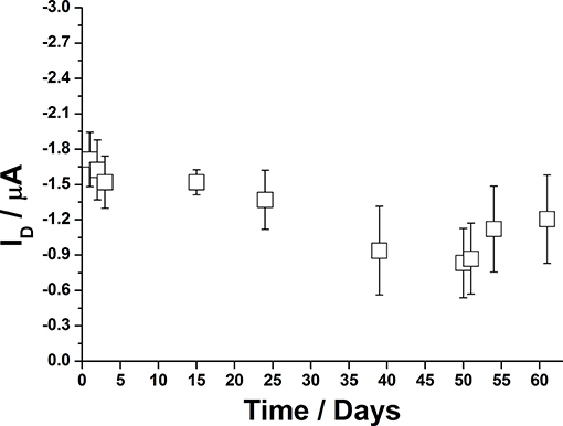
Figure 10. Long-term stability of P3HT based EGOFETs, stored with a protecting layer of agarose gel. Error bars refer to one standard deviation calculated on three devices.
Conclusions
The investigation of the degradation processes occurring on P3HT film serving as semiconducting channel material in water-gated field-effect-transistors was carried out adopting the measurement protocols successfully set in single-molecule biosensing experiments. A benchmark polymer without any additional treatment was used in the development of water-gated FETs to study its reliability on prolonged use. It was observed that no hysteresis and limited leakage currents were achieved not only by operating the OS in a voltage range where typical parasitic electrochemical processes are absent (i.e., water electrolysis, polymer oxidation), but also by the suitable set up of the measuring protocol. Furthermore, it was shown that water incubation more than operation in cycling mode is responsible for the initial abrupt current loss occurring in the first 20 h. Such behavior accounts for the unavoidable presence of water in between the polymer chains. The role of degradation in water for long period was also highlighted by SEM, AFM, and XPS analyses demonstrating that roughness increases and additional hydroxyl moieties are present. A model of P3HT EGOFET degradation operating the device over 1 week continuously was proposed suggesting that the current loss is due to the VT shift by a bi-exponential decay. On the other hand, P3HT based devices could keep their electrical performance over a prolonged period if stored under ambient conditions with a protecting layer of agarose gel. Though we are aware that particular conditions and materials were applied in this study, this work can be a guide to investigate aspects of EGOFET device stability which could be critical for their use in transistor biosensors.
Data Availability Statement
All datasets generated for this study are included in the manuscript/Supplementary Files.
Author Contributions
RP, KM, EM, and AT carried out the EGOFET fabrication, including measuring cell design, and the electrical characterization. RP wrote the first draft of the manuscript and performed XPS characterization. KM set up the measuring protocol. CD and GS were responsible for interdigitated electrode fabrication, SEM, and AFM analyses. NC contributed to the investigation of spurious electrochemical processes. LT supervised the overall study, coordinated the team, and revised the manuscript as approved by all the authors.
Conflict of Interest
The authors declare that the research was conducted in the absence of any commercial or financial relationships that could be construed as a potential conflict of interest.
Acknowledgments
RP acknowledges the financial support of Fondo di Sviluppo e Coesione 2007-2013–APQ Ricerca Regione Puglia Programma regionale a sostegno della specializzazione intelligente e della sostenibilità sociale ed ambientale–Future In Research project #B164PG8 (BEND: Biosensori elettronici intelligenti per la diagnosi precoce di malattie neurodegenerative). Additional grants are acknowledged for partial financial support: SiMBiT: Single molecule bio-electronic smart system array for clinical testing funded by the European Commission under H2020 program, grant #824946, MIUR PON - e-DESIGN: Combination of Design, Electronics and Multifunctional Materials for New Aesthetic Components (ARS01_01158).
Supplementary Material
The Supplementary Material for this article can be found online at: https://www.frontiersin.org/articles/10.3389/fchem.2019.00667/full#supplementary-material
References
Algarni, S. A., Althagafi, T. M., Naim, A. A., and Grell, M. (2016). A water-gated organic thin film transistor as a sensor for water-borne amines. Talanta 153, 107–110. doi: 10.1016/j.talanta.2016.01.068
Angione, M. D., Cotrone, S., Magliulo, M., Mallardi, A., Altamura, D., Giannini, C., et al. (2012). Interfacial electronic effects in functional biolayers integrated into organic field-effect transistors. Proc. Natl. Acad. Sci.U.S.A. 109, 6429–6434. doi: 10.1073/pnas.1200549109
Beatrup, D., Wade, J., Biniek, L., Bronstein, H., Hurhangee, M., Kim, J.-S., et al. (2014). Polaron stability in semiconducting polymer neat films. Chem. Commun. 50, 14425–14428. doi: 10.1039/C4CC06193D
Bellani, S., Fazzi, D., Bruno, P., Giussani, E., Canesi, E. V., Lanzani, G., et al. (2014). Reversible P3HT/oxygen charge transfer complex identification in thin films exposed to direct contact with water. J. Phys. Chem. C 118, 6291–6299. doi: 10.1021/jp4119309
Bobbert, P. A., Sharma, A., Mathijssen, S. G., Kemerink, M., and de Leeuw, D. M. (2012). Operational stability of organic field-effect transistors. Adv. Mater. 24, 1146–1158. doi: 10.1002/adma.201104580
Cramer, T., Campana, A., Leonardi, F., Casalini, S., Kyndiah, A., Murgia, M., et al. (2013). Water-gated organic field effect transistors – opportunities for biochemical sensing and extracellular signal transduction. J. Mater. Chem. B 1, 3728–3741. doi: 10.1039/c3tb20340a
de Leeuw, D. M., Simenon, M. M. J., Brown, A. R., and Einerhand, R. E. F. (1997). Stability of n-type doped conducting polymers and consequences for polymeric microelectronic devices. Int. Conf. Sci. Technol. Synth. Met. 87, 53–59. doi: 10.1016/S0379-6779(97)80097-5
Hwang, D. K., Fuentes-Hernandez, C., Kim, J., Potscavage, W. J., Kim, S.-J., and Kippelen, B. (2011). Top-gate organic field-effect transistors with high environmental and operational stability. Adv. Mater. 23, 1293–1298. doi: 10.1002/adma.201004278
Jia, X., Fuentes-Hernandez, C., Wang, C.-Y., Park, Y., and Kippelen, B. (2018). Stable organic thin-film transistors. Sci. Adv. 4:eaao1705. doi: 10.1126/sciadv.aao1705
Kergoat, L., Battaglini, N., Miozzo, L., Piro, B., Pham, M.-C., Yassar, A., et al. (2011). Use of poly(3-hexylthiophene)/poly(methyl methacrylate) (P3HT/PMMA) blends to improve the performance of water-gated organic field-effect transistors. Org. Electron. 12, 1253–1257. doi: 10.1016/j.orgel.2011.04.006
Kergoat, L., Herlogsson, L., Braga, D., Piro, B., Pham, M.-C., Crispin, X., et al. (2010). A water-gate organic field-effect transistor. Adv. Mater. 22, 2565–2569. doi: 10.1002/adma.200904163
Kim, S. H., Hong, K., Xie, W., Lee, K. H., Zhang, S., Lodge, T. P., et al. (2013). electrolyte-gated transistors for organic and printed electronics. Adv. Mater. 25, 1822–1846. doi: 10.1002/adma.201202790
Knopfmacher, O., Hammock, M. L., Appleton, A. L., Schwartz, G., Mei, J., Lei, T., et al. (2014). Highly stable organic polymer field-effect transistor sensor for selective detection in the marine environment. Nat. Commun. 5:2954. doi: 10.1038/ncomms3954
Lee, E. K., Lee, M. Y., Park, C. H., Lee, H. R., and Oh, J. H. (2017). Toward environmentally robust organic electronics: approaches and applications. Adv. Mater. 29:1703638. doi: 10.1002/adma.201703638
Li, H., Shi, W., Song, J., Jang, H.-J., Dailey, J., Yu, J., et al. (2018). Chemical and biomolecule sensing with organic field-effect transistors. Chem. Rev. 119, 3–35. doi: 10.1021/acs.chemrev.8b00016
Macchia, E., Alberga, D., Manoli, K., Mangiatordi, G. F., Magliulo, M., Palazzo, G., et al. (2016). Organic bioelectronics probing conformational changes in surface confined proteins. Sci. Rep. 6:28085. doi: 10.1038/srep28085
Macchia, E., Manoli, K., Holzer, B., Di Franco, C., Ghittorelli, M., Torricelli, F., et al. (2018a). Single-molecule detection with a millimetre-sized transistor. Nat. Commun. 9:3223. doi: 10.1038/s41467-018-05235-z
Macchia, E., Manoli, K., Holzer, B., Di Franco, C., Picca, R. A., Cioffi, N., et al. (2019a). Selective single-molecule analytical detection of C-reactive protein in saliva with an organic transistor. Anal. Bioanal. Chem. 411, 4899–4908. doi: 10.1007/s00216-019-01778-2
Macchia, E., Romele, P., Manoli, K., Ghittorelli, M., Magliulo, M., Kovács-Vajna, Z. M., et al. (2018b). Ultra-sensitive protein detection with organic electrochemical transistors printed on plastic substrates. Flex. Print. Electron. 3:034002. doi: 10.1088/2058-8585/aad0cb
Macchia, E., Tiwari, A., Manoli, K., Holzer, B., Ditaranto, N., Picca, R. A., et al. (2019b). Label-free and selective single-molecule bioelectronic sensing with a millimeter-wide self-assembled monolayer of anti-immunoglobulins. Chem. Mater. 31, 6476–6483. doi: 10.1021/acs.chemmater.8b04414
Macchia, E., Zak, A., Picca, R. A., Manoli, K., Di Franco, C., Cioffi, N., et al. (2018c). improved performance p-type polymer (P3HT) / n-type nanotubes (WS2) electrolyte gated thin-film transistor. MRS Adv. 3, 1525–1533. doi: 10.1557/adv.2018.311
Magliulo, M., Mallardi, A., Mulla, M. Y., Cotrone, S., Pistillo, B. R., Favia, P., et al. (2013). Electrolyte-gated organic field-effect transistor sensors based on supported biotinylated phospholipid bilayer. Adv. Mater. 25, 2090–2094. doi: 10.1002/adma.201203587
Manoli, K., Magliulo, M., Mulla, M. Y., Singh, M., Sabbatini, L., Palazzo, G., et al. (2015). printable bioelectronics to investigate functional biological interfaces. Angew. Chem. Int. Ed. 54, 12562–12576. doi: 10.1002/anie.201502615
Manoli, K., Patrikoussakis, M. M., Magliulo, M., Dumitru, L. M., Mulla, M. Y., Sabbatini, L., et al. (2014). Pulsed voltage driven organic field-effect transistors for high stability transient current measurements. Org. Electron. 15, 2372–2380. doi: 10.1016/j.orgel.2014.06.034
Miyadera, T., Minari, T., Wang, S. D., and Tsukagoshi, K. (2008). Dynamic bias stress current instability caused by charge trapping and detrapping in pentacene thin film transistors. Appl. Phys. Lett. 93:213302. doi: 10.1063/1.3037213
Mulla, M. Y., Tuccori, E., Magliulo, M., Lattanzi, G., Palazzo, G., Persaud, K., et al. (2015). Capacitance-modulated transistor detects odorant binding protein chiral interactions. Nat. Commun. 6:6010. doi: 10.1038/ncomms7010
National Institute of Standards Technology (2012). XPS Database. NIST X-Ray Photoelectron Spectrosc. Database Version 41. Available online at: http://srdata.nist.gov/xps
Nikolka, M., Nasrallah, I., Rose, B., Ravva, M. K., Broch, K., Sadhanala, A., et al. (2016). High operational and environmental stability of high-mobility conjugated polymer field-effect transistors through the use of molecular additives. Nat. Mater. 16, 356–362. doi: 10.1038/nmat4785
Panzer, M. J., and Frisbie, C. D. (2008). Exploiting ionic coupling in electronic devices: electrolyte-gated organic field-effect transistors. Adv. Mater. 20, 3177–3180. doi: 10.1002/adma.200800617
Panzer, M. J., Newman, C. R., and Frisbie, C. D. (2005). Low-voltage operation of a pentacene field-effect transistor with a polymer electrolyte gate dielectric. Appl. Phys. Lett. 86:103503. doi: 10.1063/1.1880434
Picca, R. A., Manoli, K., Luciano, A., Sportelli, M. C., Palazzo, G., Torsi, L., et al. (2018). Enhanced stability of organic field-effect transistor biosensors bearing electrosynthesized ZnO nanoparticles. Sens. Actuators B Chem. 274, 210–217. doi: 10.1016/j.snb.2018.07.128
Picca, R. A., Sportelli, M. C., Hötger, D., Manoli, K., Kranz, C., Mizaikoff, B., et al. (2015). Electrosynthesis and characterization of ZnO nanoparticles as inorganic component in organic thin-film transistor active layers. Electrochim. Acta 178, 45–54. doi: 10.1016/j.electacta.2015.07.122
Porrazzo, R., Bellani, S., Luzio, A., Lanzarini, E., Caironi, M., and Antognazza, M. R. (2014). Improving mobility and electrochemical stability of a water-gated polymer field-effect transistor. Org. Electron. 15, 2126–2134. doi: 10.1016/j.orgel.2014.06.002
Salleo, A., Endicott, F., and Street, R. A. (2005). Reversible and irreversible trapping at room temperature in poly(thiophene) thin-film transistors. Appl. Phys. Lett. 86:263505. doi: 10.1063/1.1968437
Sharma, A., Mathijssen, S. G. J., Cramer, T., Kemerink, M., de Leeuw, D. M., and Bobbert, P. A. (2010). Anomalous current transients in organic field-effect transistors. Appl. Phys. Lett. 96:103306. doi: 10.1063/1.3339879
Sirringhaus, H. (2005). Device physics of solution-processed organic field-effect transistors. Adv. Mater. 17, 2411–2425. doi: 10.1002/adma.200501152
Sirringhaus, H. (2009). Reliability of organic field-effect transistors. Adv. Mater. 21, 3859–3873. doi: 10.1002/adma.200901136
Sportelli, M. C., Picca, R. A., Manoli, K., Re, M., Pesce, E., Tapfer, L., et al. (2017). Surface analytical characterization of Streptavidin/poly(3–hexylthiophene) bilayers for bio-electronic applications. Appl. Surf. Sci. 420, 313–322. doi: 10.1016/j.apsusc.2017.05.086
Surya, S. G., Raval, H. N., Ahmad, R., Sonar, P., Salama, K. N., and Rao, V. R. (2019). Organic field effect transistors (OFETs) in environmental sensing and health monitoring: A review. TrAC Trends Anal. Chem. 111, 27–36. doi: 10.1016/j.trac.2018.11.027
Torsi, L., and Dodabalapur, A. (2005). Organic thin-film transistors as plastic analytical sensors. Anal. Chem. 77, 380A−387A. doi: 10.1021/ac053475n
Torsi, L., Magliulo, M., Manoli, K., and Palazzo, G. (2013). Organic field-effect transistor sensors: a tutorial review. Chem. Soc. Rev. 42, 8612–8628. doi: 10.1039/c3cs60127g
Wade, J., Wood, S., Beatrup, D., Hurhangee, M., Bronstein, H., McCulloch, I., et al. (2015). Operational electrochemical stability of thiophene-thiazole copolymers probed by resonant Raman spectroscopy. J. Chem. Phys. 142:244904. doi: 10.1063/1.4923197
Wang, D., Noël, V., and Piro, B. (2016). Electrolytic gated organic field-effect transistors for application in biosensors—a review. Electronics 5:9. doi: 10.3390/electronics5010009
Yu, D., Yang, Y.-Q., Chen, Z., Tao, Y., and Liu, Y.-F. (2016). Recent progress on thin-film encapsulation technologies for organic electronic devices. Opt. Commun. 362, 43–49. doi: 10.1016/j.optcom.2015.08.021
Zhang, Q., Leonardi, F., Casalini, S., Temiño, I., and Mas-Torrent, M. (2016). High performing solution-coated electrolyte-gated organic field-effect transistors for aqueous media operation. Sci. Rep. 6:39623. doi: 10.1038/srep39623
Zhang, X.-H., Tiwari, S. P., and Kippelen, B. (2009). Pentacene organic field-effect transistors with polymeric dielectric interfaces: performance and stability. Org. Electron. 10, 1133–1140. doi: 10.1016/j.orgel.2009.06.001
Keywords: poly-3-hexylthiophene, electrolyte-gated OFET, degradation, pulsed mode, biosensors
Citation: Picca RA, Manoli K, Macchia E, Tricase A, Di Franco C, Scamarcio G, Cioffi N and Torsi L (2019) A Study on the Stability of Water-Gated Organic Field-Effect-Transistors Based on a Commercial p-Type Polymer. Front. Chem. 7:667. doi: 10.3389/fchem.2019.00667
Received: 21 January 2019; Accepted: 18 September 2019;
Published: 10 October 2019.
Edited by:
Wolfgang Knoll, Austrian Institute of Technology (AIT), AustriaReviewed by:
Maria Daniela Angione, Trinity College Dublin, IrelandSven Ingebrandt, RWTH Aachen University, Germany
Copyright © 2019 Picca, Manoli, Macchia, Tricase, Di Franco, Scamarcio, Cioffi and Torsi. This is an open-access article distributed under the terms of the Creative Commons Attribution License (CC BY). The use, distribution or reproduction in other forums is permitted, provided the original author(s) and the copyright owner(s) are credited and that the original publication in this journal is cited, in accordance with accepted academic practice. No use, distribution or reproduction is permitted which does not comply with these terms.
*Correspondence: Rosaria Anna Picca, cm9zYXJpYS5waWNjYUB1bmliYS5pdA==; Luisa Torsi, bHVpc2EudG9yc2lAdW5pYmEuaXQ=