 Peter Byrley
 Ming Liu2
 Ruoxue Yan
- 1Department of Chemical and Environmental Engineering, University of California, Riverside, Riverside, CA, United States
- 2Department of Electrical and Computer Engineering, University of California, Riverside, Riverside, CA, United States
- 3Material Science and Engineering Program, Bourns College of Engineering, University of California, Riverside, Riverside, CA, United States
Monolayer transition metal dichalcogenide (TMDs) are promising candidates for two-dimensional (2D) ultrathin, flexible, low-power, and transparent electronics and optoelectronics. However, the performance of TMD-based devices is still limited by the relatively low carrier mobility and the large contact resistance between the semiconducting 2D channel material and the contact metal electrodes. Phase-engineering in monolayer TMDs showed great promise in enabling the fabrication of high-quality hetero-phase structures with controlled carrier mobilities and heterojunction materials with reduced contact resistance. However, to date, general methods to induce phase-change in monolayer TMDs either employ highly-hostile organometallic compounds, or have limited compatibility with large-scale, cost-effective device fabrication. In this paper, we report a new photochemical method to induce semiconductor to metallic phase transition in monolayer MoS2 in a benign chemical environment, through a bench-top, cost-effective solution phase process that is compatible with large-scale device fabrication. It was demonstrated that photoelectrons produced by the band-gap absorption of monolayer MoS2 have enough chemical potential to activate the phase transition in the presence of an electron-donating solvent. This novel photochemical phase-transition mechanism advances our fundamental understanding of the phase transformation in 2D transition metal dichalcogenides (TMDs), and will open new revenues in the fabrication of atomically-thick metal-semiconductor heterostructures for improved carrier mobility and reduced contact resistance in TMD-based electronic and optoelectronic devices.
Introduction
Layered transition metal dichalcogenides (TMDs) have attracted major research interests in recent years because of their special two-dimensional layer structures and potential as high-performance functional nano-materials. The presence of a finite band gap, photo-responsivity, and outstanding electronic and optical properties make them promising candidates for optoelectronics and nanoelectronics.
Field effect transistors (FET) based on monolayer TMDs, in particular, MoS2 and WSe2, have been widely studied due to their excellent properties including high on/off ratios (exceeding 108), immunity to short channel effects, and abrupt subthreshold switching (Yoon et al., 2011; Song et al., 2013; Kappera et al., 2014a; Pradhan et al., 2014; Liu et al., 2015). To further improve the device performance, research efforts have been focused on enhancing the carrier mobilities, investigating the contact mechanisms, and limitations in carrier transport (Radisavljevic et al., 2011; Kim et al., 2012; Das et al., 2013; Gong et al., 2013; Radisavljevic and Kis, 2013; Sangwan et al., 2013; Li et al., 2017; Lv et al., 2018). Currently, the reported carrier mobilities have a wide range of variations from 1 to 400 cm2V-1s-1, depending on the fabrication method, contact resistance, and it was recently found out that they also depend on the phase of the TMD layer (Kappera et al., 2014a,b; Guo et al., 2015; Ma et al., 2015). TMDs have several different phases, including the most common 2H phase (semiconducting) and 1T phase (metallic) (van der Zande et al., 2013; Voiry et al., 2013; Zhou et al., 2013; Kappera et al., 2014a; Acerce et al., 2015; Tang and Jiang, 2015). These two phases have different electronic band structures and other properties such as carrier mobility and optical absorption efficiency in the visible range (Guo et al., 2015; Xiong et al., 2015). Theoretical studies have put the electron and hole mobilities in 1T-MoS2 at 6.4 × 104 cm2 V-1 s-1 and 5.7 × 104 cm2 V−1 s−1, respectively, which are about two orders of magnitude higher than in 1H-MoS2 (1.2 × 102 cm2 V-1 s-1 for electrons and 3.8 × 102 cm2 V-1 s-1 for holes) (Kan et al., 2014). This large enhancement was attributed to the reduction of the electron (hole) effective mass from 0.49 me (0.60 mh) to 0.12 me (0.05 mh) when the 2H-MoS2 is converted to 1T-MoS2 (Kan et al., 2014). It has also been shown that the 1T-phase MoS2 can significantly decrease the contact resistance of monolayer-MoS2-based transistors to ~200–300 Ω-μm at the room temperature from ~1,000 Ω-μm in devices using pure 2H-MoS2 (Kappera et al., 2014a), an impressive level that is getting close to the best contact resistance between graphene and palladium reported by IBM (110 ± 20 Ω μm at 6 K) (Xia et al., 2011). Phase-engineering in monolayer TMDs has offered an extra handle in performance optimization of TMDs-based nano-electronics and optoelectronic by enabling the preparation of novel structures, such as high-quality mix-phase material with controllable carrier mobility and patternable heterojunction materials (Duan et al., 2014; Duesberg, 2014; Gong et al., 2014; Huang et al., 2014; Mahjouri-Samani et al., 2015; Zeng et al., 2015; Zheng et al., 2015).
Traditionally, 2H to 1T phase transition is realized through alkali metal (Li+, Na+, or K+) intercalation using highly reductive organometallic compounds, such as n- or t-butylithium, and has been studied for about three decades in bulk MoS2 (Py and Haering, 1983; Zheng et al., 2014; Mahjouri-Samani et al., 2015; Tan and Zhang, 2015). In a typical synthesis, MoS2 is intercalated with lithium to form the reduced LixMoSn phase with expanded lattice, which can be exfoliated into monolayer films by ultrasound-assisted hydration process. The reduced LixMoSn phase has the same octahedral symmetry as 1T-MoS2, and the subsequent deintercalation preserves the octahedral structure, yielding a metastable 1T metallic phase. Recently, this method has been extended to the preparation of mono- or few layer TMDs (Eda et al., 2011; Zeng et al., 2011; Cheng et al., 2014; Dong et al., 2014; Eng et al., 2014; Knirsch et al., 2015). The major drawback of this technique is the long lithiation time (e.g., a range of 2 h to 3 days soaking at 100°C), and the poor film quality due to the damage due to the violent reaction between lithium and water. The use of expensive and hostile organometallic compounds requires an oxygen- and water-free processing environment and is highly explosive, which leads to cost and safety concerns as the phase-engineering process is scaled up. Thus, there is a lot of interest in developing a method to induce phase change in monolayer MoS2 that is safer, more time efficient and lower cost. Several alternative methods have been proposed to induce the 2H to 1T phase transition in monolayer MoS2, including strain, electron beam, plasma bombardment, and plasmonic hot electron induction (Enyashin et al., 2011; Kang et al., 2014; Lin et al., 2014; Katagiri et al., 2016; Zhu et al., 2017). However, in general, a clean, low cost and scalable phase engineering technique is still not available.
In this paper, we report a new photochemical route to induce 2H to 1T phase transition in MoS2 monolayers in a benign chemical environment. We find that photoelectrons produced by the band-gap absorption of monolayer MoS2 have enough chemical potential to activate the phase transition in the presence of a hole scavenger. This novel photochemical phase-transition mechanism was systematically investigated by in-situ 2D photoluminescence (PL) mapping, in-situ Raman, atomic force microscopy (AFM), and X-ray photoelectron spectroscopy (XPS) and control experiments demonstrating the dependence of the phase-change process on the redox environment.
Results and Discussion
Figure 1 shows the mechanistic illustration of the photochemical phase-transition mechanism. As shown in Figure 1A, the 2H-MoS2 has the D3h symmetry, and its crystal field splits the five Mo 4d orbitals into three groups (Figure 1B, left): an a orbital (), which is the most stable of all, followed by two degenerate e' orbitals (4dxz and 4dyz) and two degenerate e” ( and 4dyz) orbitals. The Mo ion is in the +4 oxidation state and has two 4d electrons, both residing in the lowest lying and leaving the higher energy 4d orbitals empty. The complete occupation of the , which correspond to the valance band in its electronic band structure, renders 2H semiconducting. On the contrary, 1T-MoS2 has a centrosymmetric Oh symmetry (Figure 1A, right), which splits the Mo 4d orbitals into 2 groups (Figure 1B, right): the lower energy t2g orbitals (4dxy, 4dxz, and 4dyz) and the higher energy orbitals ( and ). At the ground state, the two Mo 4d-electrons has to fill in 2 of the 3 degenerate t2g orbitals instead. The incomplete occupation of the 1T t2g orbitals indicates partially occupied valence band, making 1T phase metallic (Chhowalla et al., 2015). The S 3p states do not influence the electronic structure of the materials, as they are located approximately 3 eV away from the Fermi level. Since the orbital in 2H-MoS2 is slightly more stable than the t2g orbitals in 1T-MoS2, the total energy of Mo 4d-electrons are also lower, rendering 2H phase thermodynamically favored.
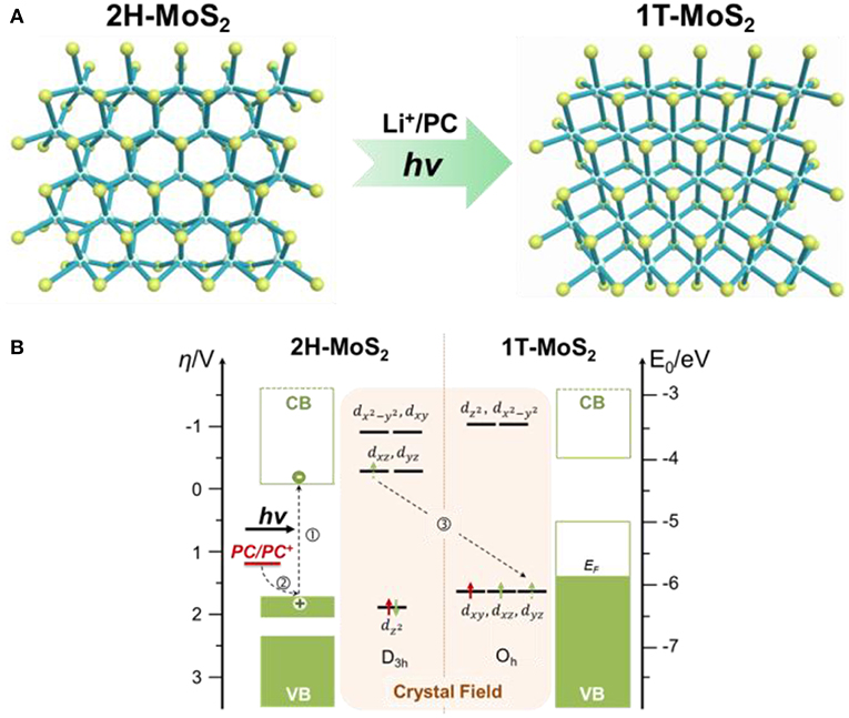
Figure 1. Mechanistic illustration of the photochemical 2H to 1T phase transition in monolayer MoS2. (A) Atomic structures of 2H- and 1T-MoS2. (B) Energy diagram of 2H- and 1T-MoS2 and the corresponding crystal fields of Mo 4d orbitals. The proposed route of photochemical phase transition is marked by dotted arrows. Step 1, photo absorption to generate photo electrons in the conduction band (CB) and photo holes in the valence band (VB) of 2H-MoS2 (left). Step 2, electron donation from the hole scavenger, propylene carbonate (PC), whose redox potential falls above the valence band of the 2H-MoS2. The photo-assisted electron injection to the conduction band of 2H-MoS2 destabilizes the 2H phase. Step 3, phase transition from the destabilized 2H phase to the thermodynamically more stable 1T phase (for d3 configuration). The green arrows on the 4d orbitals represent the original 4d electrons on the Mo atom, while the red arrows represent the extra electron donated by the hole scavenger molecule.
When the 2H-MoS2 accept an extra electron, that electron is forced into the high energy e' orbitals, which is much higher than due to the large crystal field stabilization energy in D3h symmetry, destabilizing 2H phase. On the contrary, the triply degenerate t2g orbitals in 1T phase would be able to accommodate all three Mo 4d electrons and reach the stable half-filled configuration. Since t2g in 1T-MoS2 is much lower in energy than e' orbitals in 2H-MoS2, the total energy of the d3 configuration is considerably lower in 1T phase, thus allowing phase conversion to occur (Enyashin and Seifert, 2012; Cheng et al., 2014; Kan et al., 2014). This forms the foundation of electron-injection-induced MoS2 phase transition. Instead of using the hostile reductant like butylithium in the chemical intercalation method, or direct physical electron injections using high-energy electron beams or plasmonic hot-electrons, in the photochemical route, low energy visible light was used to provide the extra electron by generating photoelectrons in 2H-MoS2.
As shown in Figure 1B, visible light with a photon energy beyond the bandgap of monolayer 2H-MoS2 (~1.8eV) excites a valence band () electron into the conduction band, which corresponds to the degenerate e' orbitals (4dxz and 4dyz). The photo-generated hole left behind in the state is filled by an electron transferred from a hole scavenging molecule, whose oxidation potential is higher than , or the top of the valence band. Effectively, this is a photo-reduction process, in which the electron injected into MoS2 is supplied by the hole scavenger and the activation energy is provided by a visible photon. In our demonstration, the hole scavenger used is propylene carbonate (PC), the oxidation potential of which is 1.2V vs. NHE (Kanamura et al., 1995), which converts to −5.6 eV vs. vacuum. This is slightly above the valence band of monolayer 2H-MoS2, which is roughly around −6.5 eV below vacuum (Schlaf et al., 1999; Choi et al., 2013; Furchi et al., 2014). The reduced MoS2 goes through phase-transition to the more-stable 1T structure, which was then stabilized by Li+ ions, which balance the negative charges on reduced 1T-MoS2. The Li+ ion here is not from harsh organolithium, but is from a mild lithium salt (LiPF6) dissolved in PC.
Figure 2 shows the in situ 2D photoluminescence mapping that follows the photochemical phase transition of 2H-MoS2 monolayer flakes grown with chemical vapor deposition (CVD) on a SiO2 substrate. The substrate was encapsulated in a liquid chamber with 1M PC solution of LiPF6 and sealed to prevent evaporation. The MoS2 monolayer flakes were then scanned with a tightly-focused 532 nm laser. With a photon energy higher than the band gap of monolayer MoS2, the laser served dual purposes: providing activation energy for the photo-reduction and exciting MoS2 photoluminescence, the quenching of which serves an in-situ indicator of the formation of the 1T metallic phase (Eda et al., 2011). The laser power was maintained at 0.76 mW/μm2 (1.2 μm spot size) to prevent photodamage and an accumulation time of 1 s per pixel was used for all 2D scanning. Figures 2A,B show the result of the 1st and 5th laser scan of the same MoS2 flake (on the left), which shows a clear PL quenching which suggests the increase of the metallic 1T-phase component. The entire 5 scans were compiled in Figure S1, which shows the gradual PL quenching of the left domain with time evolution. It is worth mentioning that scan 3 and 4 was stopped early so the total illumination times of the two MoS2 flakes on the right are shorter than the domain on the left. The different degrees of PL quenching among the MoS2 flakes clearly demonstrates the correlation between the PL intensity and the duration of light exposure. Figure 2B shows the PL spectra of another MoS2 flake, collected at different times during continued illumination, also showing a clear time-dependence in PL quenching on light exposure. Figure S2 further shows that the PL intensity decays exponentially with the illumination time. AFM images taken before and after laser exposure (0.76 mW/μm2, 240 s) in LiPF5/PC solution (Figure 2C) indicate that the sample was not damaged by laser ablation. This is consistent with previous reports that the thermal effect is insignificant at such low power densities and laser thinning requires at least 20 mW/μm2 in laser power (Najmaei et al., 2012; Hu et al., 2017).
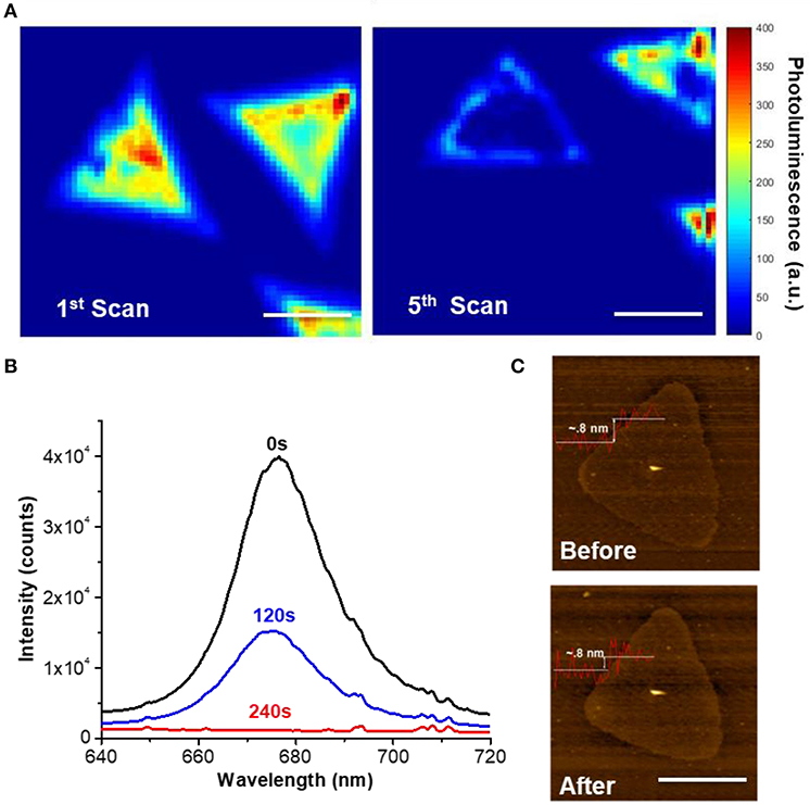
Figure 2. Optical and morphological characterization of the photochemical phase change of monolayer CVD MoS2. (A) in-situ 2D photoluminescence (PL) imaging following the photochemical phase change of a single MoS2 monolayer flake (left). The left image shows the initial scanning and the right image shows the 5th consecutive scan after 2 h of imaging with a laser power of 0.76 mW/μm2 at 532 nm and 1 s/pixel. The right image was slightly drifted/rotated with respect to the right image during alignment and slight distortion was also observed due to piezo hysteresis. Scale bar: 10 μm. (B) Time dependent PL spectra of a MoS2 flake during illumination showing clear PL quenching (5 s accumulation time). (C) AFM image of the same MoS2 monolayer flake before and after the photochemical phase change showing no sign of photodamage to the structure integrity. Scale bar: 10 μm.
We have observed considerable variations in different CVD MoS2 samples. The CVD grown MoS2 flakes are highly prone to chalcogen deficiency because of the high volatility of chalcogenides, and therefore contain an abundance of chalcogen vacancies inherently creates structural defects that affect carrier diffusion and activate non-radiative recombination channels (Zhou et al., 2013; Hong et al., 2015). Depending on the growth parameter, such as the amount and distance of solid precursors, growth temperature and duration, the film quality can vary significantly from batch to batch and even at different positions on the same substrate (Zafar et al., 2017). These variations affect the optical behavior of the sample as well as any photo-induced processes, however, there have been increasing research attentions directed on the defect-controlled growth of high-quality MoS2 films (Chen et al., 2015; Tao et al., 2017). The continued improvement in MoS2 synthesis will provide more precision in the optimization of the photochemical phase transition method.
In-situ confocal Raman spectroscopy was carried out to examine the structure evolution of the MoS2 flakes. The Raman spectra (Figure 3) show characteristic peaks at 382 and 402 cm−1, which can be assigned to the and A1g phonon modes, respectively (Sun et al., 2014). Chemically exfoliated 1T-MoS2 using butyllithium solution shows distinct Raman signature of superlattices at 150 cm−1 (J1), 226 cm−1 (J2), and 333 cm−1 (J3)(Yang et al., 1991). The appearance of these superlattice peaks has been used as the indication of the 1T phase (Kang et al., 2014; Kappera et al., 2014b; Zhu et al., 2017), however, it is also worth noting that their relative intensities, and even whether or not they appear together in mixed phase monolayer MoS2 samples are not in agreement across the literature. For example, 1T-MoS−2 flakes produced with 40 s Ar plasma treatment has 40% 1T phase, but J1 and J2 intensities are both quite similar to the pristine sample before treatment, leaving J3 is the most prominent peak (Zhu et al., 2017). In a separate case, 48 hours of n-butyl lithium treatment yields 70% of 1T phase and its Raman spectra shows a very prominent J2 peak, a very weak J3, and no J1(Kappera et al., 2014b). In our case, the lowest frequency J1 peak is too weak to be discerned from the residue laser background which takes off quickly below 175 cm−1. The J2 peak is very close to LA mode of MoS2 at 227 cm−1, which also makes it difficult to stand out. However, with the increasing illumination time, a new J3 peak was clearly observed after 20 min under a laser illumination power of 0.14 mW/μm2, clearly indicative of a 1T phase formation. We have also observed a new peak at ~370 cm−1, which was also seen in chemically exfoliated 1T-MoS2 together with the superlattice peaks, however, its structural origin was not clear (Yang et al., 1991). The broadening and intensity attenuation of peak was not obvious, indicating a partial phase-change under this illumination condition, without the significant loss of the D3h symmetry (Yang et al., 1991). We want to point out here that the degree of phase change is limited in the in-situ confocal Raman measurement because of a limited illumination power attainable at the sample surface and the stage drifting of the confocal Raman. However, the presence of characteristic 1T-MoS2 Raman peaks at the low frequency region supports the PL measurement result.
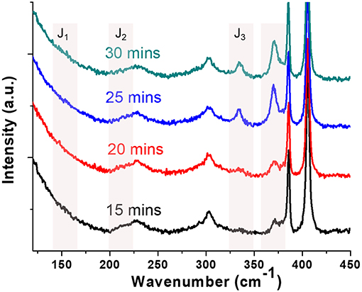
Figure 3. In-situ Raman spectra following the time evolution of a monolayer MoS2 flake during photochemical phase change. Two new peaks (330 and 370 cm−1) indicative of the 1T phase appeared with increasing illumination time (532 nm, 0.14 mW/μm2). The 19.8 cm−1 distance between the and A1g peaks indicates that the sample is a MoS2 monolayer.
X-ray photoelectron spectroscopy (XPS) provides additional evidence of the formation of 1T phase through the photochemical phase transition process. Figure 4 shows the select-area XPS spectra of the as-synthesized CVD monolayer MoS2 flake (top) and a CVD MoS2 sample phase-modified with the photochemical method. The MoS2 flake was illuminated with a 532 nm laser (~0.2 mW/μm2, 1.2 μm spot size) for 30 min in the presence of 1M LiPF4/PC solution. The XPS measurement was performed with an AXIS Supra (Kratos Instruments) using a 500 mm Rowland circle monochromated Al Ka x-ray source and an aperture of 20 μm diameter for select area measurement. All spectra were calibrated by the C 1 s peak at 284.5 eV (see Figure S3). The peaks around 230 and 233 eV, corresponding to the Mo4+ 3d5/2 and Mo4+ 3d3/2 components in 2H-MoS2, shifted slightly but distinctly to lower energies after the photochemical process, important evidence of the presence of the 1T phase (Eda et al., 2011; Cai et al., 2015). For the as-made 2H-MoS2, the XPS intensity goes back to the baseline between peaks (234 eV and 231 eV), whereas the phase-modified sample shows clear peak broadening on the low energy side and the intensity no longer goes back to the baseline at these locations, also indicating the presence of additional peaks. The deconvolution of Mo and S XPS peaks reveals 1T peaks at lower energy along with the original 2H peaks, and the relative content of 1T phase is estimated to be ~15% for this particular MoS2 flake. Considering the laser spot size of 1.2 μm and the XPS aperture of 20 μm, the illuminated region accounts for only a tiny fraction (0.3%) of the XPS probed area. The measured spectrum represents the averaged results over the entire probed area, which indicates that the photochemical phase-modification can go far beyond the illuminated region, possibly due to exciton/charge carrier diffusion and laser scattering in the liquid chamber.
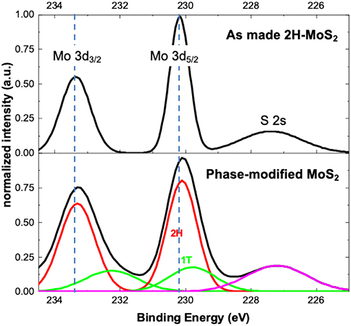
Figure 4. XPS spectra of as-synthesized and phase-modified monolayer MoS2. The phase-modified MoS2 sample (bottom black curve) shows a distinct shift and peak broadening in the Mo 3d3/2 and 3d5/2 binding energies, indicating the presence of 1T phases.
In order to further validate the proposed mechanism, the effect of different experimental parameters, such as the presence of Li+ ion, the illumination wavelength, the redox potentials of hole scavengers, were studied. Figure 5 summarized the photoluminescence (PL) spectra measured on single CVD-MoS2 monolayer flakes before and after 1 h of laser illumination under different conditions. The powers of the illumination laser and the excitation laser used for PL measurement, as well as the accumulation time of the PL spectra, was kept the constant for all control experiments. Figure 5A shows the expected PL quenching on a single MoS2 flake induced by 532 nm laser illumination in 1M LiPF6-PC solution, indicative of the semiconductor to metal phase transition. As illustrated in Figure 5E, the 532 nm laser has a photo-energy of 2.33 eV, large enough to bridge the 1.8 eV bandgap of monolayer MoS2 and excite photoelectrons that destabilize the 2H phase. The photogenerated holes left behind in the valence band were filled by electrons transferred from the PC, whose redox potential sits above the top of the MoS2 valence band. On the contrary, if the photon energy of the illumination laser is lower than the MoS2 bandgap or the redox potential of the hole scavenger sits below the top of the MoS2 valence band, no significant PL quenching was observed, as shown in Figures 5B,C. The 785 nm laser has a photon energy of 1.58 eV, not enough excite photoelectrons into the conduction band of monolayer 2H-MoS2. The acetonitrile (AN) solvent, which is more stable against oxidation than PC, has an oxidation potential of >2.6 V vs. NHE (Portis et al., 1972), which converts to −7.0 eV vs. vacuum, lower than the valence band top of the monolayer 2H-MoS2 (−6.5 eV below vacuum), and unable to function as an efficiency electron donator (e.g., hole scavenger). We have also observed that the Li+ also plays a critical role in the photochemical phase transition mechanism. As shown in Figure 5D, PL quenching was not observed with pure PC and no Li+ to stabilize the photoreduced MoS2. The role of Li+ is similar to that of the chemical exfoliation method, where the chemically reduced MoS2 (by butylithium) is intercalated with Li+ ions to form a stable LixMoSn phase that has the same Oh symmetry as 1T-MoS2. After deintercalation, the octahedral structure is preserved to yield the 1T-MoS2 phase. The absorption of Li+ on photoreduced monolayer MoS2 stabilizes the negative charges and facilitates the D3h (2H) to Oh (1T) structural transition. The results of these control experiments support the proposed photochemical phase transition mechanism illustrated in Figure 1.
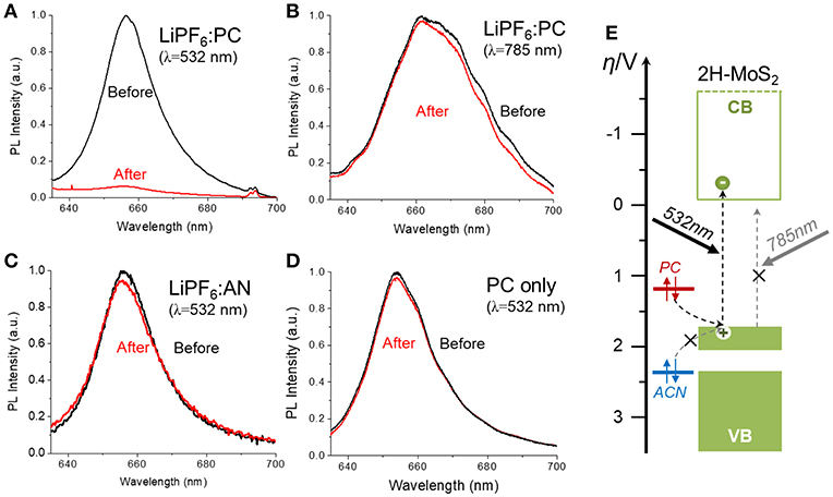
Figure 5. Measured MoS2 Photoluminescence (PL) spectra before and after 1 h of laser illumination under different conditions: (A) 1M PC solution of LiPF6 with 532 nm illumination, (B) 1M PC solution of LiPF6 with 785 nm illumination. The 785 nm laser correspond to 1.58 eV in photon energy, (C) 1M acetonitrile (AN) solution of LiPF6 with 532 nm illumination, (D) Pure PC (no Li+ ion) with 532 nm illumination. The power density of the illumination lasers in different control experiments were kept constant. Each PL spectrum was measured under 532 nm excitation for the same accumulation time (5 s), (E) The energy diagram illustrating the alignment of the 2H-MoS2 bands with redox potentials of the hole scavengers (PC and AN).
Conclusion
In summary, we have demonstrated a new photochemical route to induce 2H to 1T phase transition in MoS2 monolayers in a benign chemical environment. Photoelectrons generated by the band-gap absorption of monolayer MoS2 provide the chemical potential necessary to activate the phase transition in the presence of a proper electron-donating solvent and stabilizing metal ion. Clear evidence of phase transition was seen with a combination of characterization methods including in-situ 2D PL mapping, in-situ Raman, AFM, and XPS. This benchtop solution-based photochemical phase engineering method does not rely on glove box or any expensive clean-room technique, and is compatible with photolithography for phase-patterning on wafer-scale CVD sample. It demonstrates great promises as a clean, low cost and scalable alternative of the monolayer TMD phase engineering, and further advances the optimization and commercialization of TMD-based electronic components.
Experimental
Preparation of Monolayer MoS2 Sample
Monolayer MoS2 was synthesized on a thermal oxide (300 nm SiO2/Si) substrate at a growth temperature of 650°C in a custom CVD system using sulfur (99.98%, Sigma Aldrich) and MoO3 (99.99%, Sigma Aldrich) powder as solid precursors and Argon as carrier gas (20 sccm). After growth, the silica substrate was placed in a custom microscope liquid cell filled with 5 microliters of LiPF6: PC solution (1.0M, battery grade, Sigma Aldrich) and sealed to prevent liquid evaporation.
Photoluminescence Measurement
The PL was measured with an inverted microscope with a HORIBA iHR550 spectrophotometer and a Synapse EM CCD. A green laser (GEM 532, λ = 532 nm, Laser Quantum) was used to excite the MoS2 PL and to induce photochemical phase change. The power density of the laser is tuned by optical density filters and the reported values in the paper was measured at the sample plane. In-situ 2D mapping was conducted at 1 s/pixel using a custom LabView program. The PL spectra were measured with a 20 μm slit and 5 s accumulation time.
AFM Measurement
The topological images of the MoS2 monolayer flake before and after illumination were collected with a commercial AFM (SmartSPM, AIST-NT). The before image was measured on as-synthesized sample. After the illumination in LiPF6/PC solution, the sample was removed from the liquid cell and washed with pure propylene carbonate solvent and ethanol several times to remove excess LiPF6 on the surface. The sample was then dried and characterized by AFM immediately.
In-situ Raman Measurements
The Raman spectra were measured with a commercial confocal Raman system (LabRAM, Horiba). A green Raman laser (532 nm, 0.14 mW/μm2 measured at the sample surface) was used to excite the Raman spectra and induce the photochemical phase transition. Each Raman spectra was taken with 10 s exposure time and three accumulations.
Preparation of 1M LiPF6 in Acetonitrile
Pure LiPF6 powder (99.9%, Sigma Aldrich) was mixed in acetonitrile under an inert atmosphere for two days at high spin speed.
XPS Analysis
XPS analysis was done using a Kratos Instruments AXIS Supra with a 500 mm Rowland circle monochromated Al Ka X-ray 1486.6 eV source at the University of California, Irvine Materials Research Institute.
Data Availability
All datasets generated for this study are included the manuscript and/or the Supplementary Files.
Author Contributions
RY and ML conceived the idea and designed the experiment. PB carried out the experiment and analyzed data. PB and RY wrote the manuscript with input from all authors.
Funding
Funding for this research was provided by the National Science Foundation under Award DMR-1649795. Work by PB was partially supported by the GAANN Fellowship.
Conflict of Interest Statement
The authors declare that the research was conducted in the absence of any commercial or financial relationships that could be construed as a potential conflict of interest.
The handling editor declared a shared affiliation, though no other collaboration, with the authors PB, ML, and RY at time of review.
Supplementary Material
The Supplementary Material for this article can be found online at: https://www.frontiersin.org/articles/10.3389/fchem.2019.00442/full#supplementary-material
References
Acerce, M., Voiry, D., and Chhowalla, M. (2015). Metallic 1T phase MoS2 nanosheets as supercapacitor electrode materials. Nat. Nanotechnol. 10, 313–318. doi: 10.1038/nnano.2015.40
Cai, L., He, J., Liu, Q., Yao, T., Chen, L., Yan, W., et al. (2015). Vacancy-induced ferromagnetism of MoS2 nanosheets. J. Am. Chem. Soc. 137, 2622–2627. doi: 10.1021/ja5120908
Chen, W., Zhao, J., Zhang, J., Gu, L., Yang, Z., Li, X., et al. (2015). Oxygen-assisted chemical vapor deposition growth of large single-crystal and high-quality monolayer MoS2. J. Am. Chem. Soc. 137, 15632–15635. doi: 10.1021/jacs.5b10519
Cheng, Y., Nie, A., Zhang, Q., Gan, L. Y., Shahbazian-Yassar, R., and Schwingenschlogl, U. (2014). Origin of the phase transition in lithiated molybdenum disulfide. Acs Nano 8, 11447–11453. doi: 10.1021/nn505668c
Chhowalla, M., Voiry, D., Yang, J. E., Shin, H. S., and Loh, K. P. (2015). Phase-engineered transition-metal dichalcogenides for energy and electronics. MRS Bull. 40, 585–591. doi: 10.1557/mrs.2015.142
Choi, M. S., Lee, G. H., Yu, Y. J., Lee, D. Y., Lee, S. H., Kim, P., et al. (2013). Controlled charge trapping by molybdenum disulphide and graphene in ultrathin heterostructured memory devices. Nat. Commun. 4:1624. doi: 10.1038/ncomms2652
Das, S., Chen, H. Y., Penumatcha, A. V., and Appenzeller, J. (2013). High performance multilayer MoS2 transistors with scandium contacts. Nano Lett. 13, 100–105. doi: 10.1021/nl303583v
Dong, L., Lin, S., Yang, L., Zhang, J., Yang, C., Yang, D., et al. (2014). Spontaneous exfoliation and tailoring of MoS2 in mixed solvents. Chem. Commun. 50, 15936–15939. doi: 10.1039/C4CC07238C
Duan, X., Wang, C., Shaw, J. C., Cheng, R., Chen, Y., Li, H., et al. (2014). Lateral epitaxial growth of two-dimensional layered semiconductor heterojunctions. Nat. Nanotechnol. 9, 1024–1030. doi: 10.1038/nnano.2014.222
Duesberg, G. S. (2014). Heterojunctions in 2d semiconductors a perfect match. Nat. Mater. 13, 1075–1076. doi: 10.1038/nmat4127
Eda, G., Yamaguchi, H., Voiry, D., Fujita, T., Chen, M., and Chhowalla, M. (2011). Photoluminescence from chemically exfoliated MoS2. Nano Lett. 11, 5111–5116. doi: 10.1021/nl201874w
Eng, A. Y., Ambrosi, A., Sofer, Z., Šimek, P., and Pumera, M. (2014). Electrochemistry of transition metal dichalcogenides: strong dependence on the metal-to-chalcogen composition and exfoliation method. Acs Nano 8, 12185–12198. doi: 10.1021/nn503832j
Enyashin, A. N., and Seifert, G. (2012). Density-functional study of LixMoS2 intercalates (0 <= x <= 1). Comput. Theor. Chem. 999, 13–20. doi: 10.1016/j.comptc.2012.08.005
Enyashin, A. N., Yadgarov, L., Houben, L., Popov, I., Weidenbach, M., Tenne, R., et al. (2011). New route for stabilization of 1T-WS2 and MoS2 phases. J. Phys. Chem. C 115, 24586–24591. doi: 10.1021/jp2076325
Furchi, M. M., Pospischil, A., Libisch, F., Burgdörfer, J., and Mueller, T. (2014). Photovoltaic effect in an electrically tunable van der Waals heterojunction. Nano Lett. 14, 4785–4791. doi: 10.1021/nl501962c
Gong, C., Huang, C., Miller, J., Cheng, L., Hao, Y., Cobden, D., et al. (2013). Metal contacts on physical vapor deposited monolayer MoS. Acs Nano 7, 11350–11357. doi: 10.1021/nn4052138
Gong, Y., Lin, J., Wang, X., Shi, G., Lei, S., Lin, Z., et al. (2014). Vertical and in-plane heterostructures from WS2/MoS2 monolayers. Nat. Mater. 13, 1135–1142. doi: 10.1038/nmat4091
Guo, Y., Sun, D., Ouyang, B., Raja, A., Song, J., Heinz, T. F., et al. (2015). Probing the dynamics of the metallic-to-semiconducting structural phase transformation in MoS2 crystals. Nano Lett. 15, 5081–5088. doi: 10.1021/acs.nanolett.5b01196
Hong, J., Hu, Z., Probert, M., Li, K., Lv, D., Yang, X., et al. (2015). Exploring atomic defects in molybdenum disulphide monolayers. Nat. Commun. 6:6293. doi: 10.1038/ncomms7293
Hu, L., Shan, X., Wu, Y., Zhao, J., and Lu, X. (2017). Laser thinning and patterning of MoS2 with layer-by-layer precision. Sci. Rep. 7:15538. doi: 10.1038/s41598-017-15350-4
Huang, C., Wu, S., Sanchez, A. M., Peters, J. J., Beanland, R., Ross, J. S., et al. (2014). Lateral heterojunctions within monolayer MoSe2-WSe2 semiconductors. Nat. Mater. 13, 1096–1101. doi: 10.1038/nmat4064
Kan, M., Wang, J. Y., Li, X. W., Zhang, S. H., Li, Y. W., Kawazoe, Y., et al. (2014). Structures and phase transition of a MoS2 monolayer. J. Phys. Chem. C 118, 1515–1522. doi: 10.1021/jp4076355
Kanamura, K., Toriyama, S., Shiraishi, S., and Takehara, Z. (1995). Studies on electrochemical oxidation of nonaqueous electrolytes using in-situ ftir spectroscopy .1. The effect of type of electrode on on-set potential for electrochemical oxidation of propylene carbonate containing 1.0 Mol Dm(-3) Liclo4. J. Electrochem. Soc. 142, 1383–1389. doi: 10.1149/1.2048586
Kang, Y., Najmaei, S., Liu, Z., Bao, Y., Wang, Y., Zhu, X., et al. (2014). Plasmonic hot electron induced structural phase transition in a MoS2 monolayer. Adv. Mater. 26, 6467–6471. doi: 10.1002/adma.201401802
Kappera, R., Voiry, D., Yalcin, S. E., Branch, B., Gupta, G., Mohite, A. D., et al. (2014a). Phase-engineered low-resistance contacts for ultrathin MoS2 transistors. Nat. Mater. 13, 1128–1134. doi: 10.1038/nmat4080
Kappera, R., Voiry, D., Yalcin, S. E., Jen, W., Acerce, M., Torrel, S., et al. (2014b). Metallic 1T phase source/drain electrodes for field effect transistors from chemical vapor deposited MoS2. Apl. Mater. 2:092516. doi: 10.1063/1.4896077
Katagiri, Y., Nakamura, T., Ishii, A., Ohata, C., Hasegawa, M., Katsumoto, S., et al. (2016). Gate-tunable atomically thin lateral MoS2 schottky junction patterned by electron beam. Nano Lett. 16, 3788–3794. doi: 10.1021/acs.nanolett.6b01186
Kim, S., Konar, A., Hwang, W. S., Lee, J. H., Lee, J., Yang, J., et al. (2012). High-mobility and low-power thin-film transistors based on multilayer MoS2 crystals. Nat. Commun. 3:1011. doi: 10.1038/ncomms2018
Knirsch, K. C., Berner, N. C., Nerl, H. C., Cucinotta, C. S., Gholamvand, Z., McEvoy, N., et al. (2015). Basal-plane functionalization of chemically exfoliated molybdenum disulfide by diazonium salts. Acs Nano 9, 6018–6030. doi: 10.1021/acsnano.5b00965
Li, F., Wei, W., Zhao, P., Huang, B., and Dai, Y. (2017). Electronic and optical properties of pristine and vertical and lateral heterostructures of Janus MoSSe and WSSe. J. Phys. Chem. Lett. 8, 5959–5965. doi: 10.1021/acs.jpclett.7b02841
Lin, Y. C., Dumcenco, D. O., Huang, Y. S., and Suenaga, K. (2014). Atomic mechanism of the semiconducting-to-metallic phase transition in single-layered MoS2. Nat. Nanotechnol. 9, 391–396. doi: 10.1038/nnano.2014.64
Liu, E., Fu, Y., Wang, Y., Feng, Y., Liu, H., Wan, X., et al. (2015). Integrated digital inverters based on two-dimensional anisotropic ReS2 field-effect transistors. Nat. Commun. 6:6991. doi: 10.1038/ncomms7991
Lv, X., Wei, W., Zhao, P., Li, J., Huang, B., and Dai, Y. (2018). Tunable Schottky contacts in MSe 2/NbSe 2 (M = Mo and W) heterostructures and promising application potential in field-effect transistors. Phys. Chem. Chem. Phys. 20, 1897–1903. doi: 10.1039/C7CP07546D
Ma, Y., Liu, B., Zhang, A., Chen, L., Fathi, M., Shen, C., et al. (2015). Reversible semiconducting-to-metallic phase transition in chemical vapor deposition grown mono layer WSe2 and applications for devices. Acs Nano 9, 7383–7391. doi: 10.1021/acsnano.5b02399
Mahjouri-Samani, M., Lin, M. W., Wang, K., Lupini, A. R., Lee, J., Basile, L., et al. (2015). Patterned arrays of lateral heterojunctions within monolayer two-dimensional semiconductors. Nat. Commun. 6:7749. doi: 10.1038/ncomms8749
Najmaei, S., Liu, Z., Ajayan, P. M., and Lou, J. (2012). Thermal effects on the characteristic Raman spectrum of molybdenum disulfide (MoS2) of varying thicknesses. Appl. Phys. Lett. 100:013106. doi: 10.1063/1.3673907
Portis, L. C., Mann, C. K., and Roberson, J. C. (1972). Anodic background reaction in moist acetonitrile. Anal. Chem. 44, 294–297. doi: 10.1021/ac60310a018
Pradhan, N. R., Rhodes, D., Feng, S., Xin, Y., Memaran, S., Moon, B.-H., et al. (2014). Field-effect transistors based on few-layered alpha-MoTe2. Acs Nano 8, 5911–5920. doi: 10.1021/nn501013c
Py, M. A., and Haering, R. R. (1983). Structural destabilization induced by lithium intercalation in Mos2 and related-compounds. Can. J. Phys. 61, 76–84. doi: 10.1139/p83-013
Radisavljevic, B., and Kis, A. (2013). Mobility engineering and a metal-insulator transition in monolayer MoS2. Nat Mater. 12, 815–820. doi: 10.1038/nmat3687
Radisavljevic, B., Radenovic, A., Brivio, J., Giacometti, V., and Kis, A. (2011). Single-layer MoS2 transistors. Nat. Nanotechnol. 6, 147–150. doi: 10.1038/nnano.2010.279
Sangwan, V. K., Arnold, H. N., Jariwala, D., Marks, T. J., Lauhon, L. J., and Hersam, M. C. (2013). Low-frequency electronic noise in single-layer MoS2 transistors. Nano Lett. 13, 4351–4355. doi: 10.1021/nl402150r
Schlaf, R., Lang, O., Pettenkofer, C., and Jaegermann, W. (1999). Band lineup of layered semiconductor heterointerfaces prepared by van der Waals epitaxy: charge transfer correction term for the electron affinity rule. J. Appl. Phys. 85, 2732–2753. doi: 10.1063/1.369590
Song, J. G., Park, J., Lee, W., Choi, T., Jung, H., Lee, C. W., et al. (2013). Layer-controlled, wafer-scale, and conformal synthesis of tungsten disulfide nanosheets using atomic layer deposition. Acs Nano 7, 11333–11340. doi: 10.1021/nn405194e
Sun, Y., Liu, K., Hong, X., Chen, M., Kim, J., Shi, S., et al. (2014). Probing local strain at MX2–metal boundaries with surface plasmon-enhanced raman scattering. Nano Lett. 14, 5329–5334. doi: 10.1021/nl5023767
Tan, C., and Zhang, H. (2015). Wet-chemical synthesis and applications of non-layer structured two-dimensional nanomaterials. Nat. Commun. 6:7873. doi: 10.1038/ncomms8873
Tang, Q., and Jiang, D. E. (2015). Stabilization and band-gap tuning of the 1T-MoS2 monolayer by covalent functionalization. Chem. Mater. 27, 3743–3748. doi: 10.1021/acs.chemmater.5b00986
Tao, L., Chen, K., Chen, Z., Chen, W., Gui, X., Chen, H., et al. (2017). Centimeter-scale CVD growth of highly crystalline single-layer MoS2 film with spatial homogeneity and the visualization of grain boundaries. ACS Appl. Mater. Interfaces 9, 12073–12081. doi: 10.1021/acsami.7b00420
van der Zande, A. M., Huang, P. Y., Chenet, D. A., Berkelbach, T. C., You, Y., Lee, G. H., et al. (2013). Grains and grain boundaries in highly crystalline monolayer molybdenum disulphide. Nat. Mater. 12, 554–561. doi: 10.1038/nmat3633
Voiry, D., Yamaguchi, H., Li, J., Silva, R., Alves, D. C., Fujita, T., et al. (2013). Enhanced catalytic activity in strained chemically exfoliated WS2 nanosheets for hydrogen evolution. Nat Mater. 12, 850–855. doi: 10.1038/nmat3700
Xia, F., Perebeinos, V., Lin, Y. M., Wu, Y., and Avouris, P. (2011). The origins and limits of metal-graphene junction resistance. Nat. Nanotechnol. 6, 179–184. doi: 10.1038/nnano.2011.6
Xiong, F., Wang, H., Liu, X., Sun, J., Brongersma, M., Pop, E., et al. (2015). Li intercalation in MoS2: in situ observation of its dynamics and tuning optical and electrical properties. Nano Lett. 15, 6777–6784. doi: 10.1021/acs.nanolett.5b02619
Yang, D., Sandoval, S. J., Divigalpitiya, W. M., Irwin, J. C., and Frindt, R. F. (1991). Structure of single-molecular-layer MoS2. Phys. Rev. B 43, 12053–12056. doi: 10.1103/PhysRevB.43.12053
Yoon, Y., Ganapathi, K., and Salahuddin, S. (2011). How good can monolayer MoS2 transistors Be? Nano Lett. 11, 3768–3773. doi: 10.1021/nl2018178
Zafar, A., Nan, H., Zafar, Z., Wu, Z., Jiang, J., You, Y., et al. (2017). Probing the intrinsic optical quality of CVD grown MoS2. Nano Res. 10, 1608–1617. doi: 10.1007/s12274-016-1319-z
Zeng, Q., Wang, H., Fu, W., Gong, Y., Zhou, W., Ajayan, P. M., et al. (2015). Band engineering for novel two-dimensional atomic layers. Small 11, 1868–1884. doi: 10.1002/smll.201402380
Zeng, Z., Yin, Z., Huang, X., Li, H., He, Q., Lu, G., et al. (2011). Single-layer semiconducting nanosheets: high-yield preparation and device fabrication. Angew. Chem. Int. Edit. 50, 11093–11097. doi: 10.1002/anie.201106004
Zheng, J., Zhang, H., Dong, S., Liu, Y., Nai, C. T., Shin, H. S., et al. (2014). High yield exfoliation of two-dimensional chalcogenides using sodium naphthalenide. Nat. Commun. 5:2995. doi: 10.1038/ncomms3995
Zheng, S. J., Sun, L., Yin, T., Dubrovkin, A. M., Liu, F., Liu, Z., et al. (2015). Monolayers of WxMo1-xS2 alloy heterostructure with in-plane composition variations. Appl. Phys. Lett. 106:063113. doi: 10.1063/1.4908256
Zhou, W., Zou, X., Najmaei, S., Liu, Z., Shi, Y., Kong, J., et al. (2013). Intrinsic structural defects in monolayer molybdenum disulfide. Nano Lett. 13, 2615–2622. doi: 10.1021/nl4007479
Keywords: phase transition, photochemical, molybdenum disulfide (MoS2), transition metal dichacogenide, in situ spectroscopic characterization, XPS, Raman
Citation: Byrley P, Liu M and Yan R (2019) Photochemically Induced Phase Change in Monolayer Molybdenum Disulfide. Front. Chem. 7:442. doi: 10.3389/fchem.2019.00442
Received: 21 February 2019; Accepted: 29 May 2019;
Published: 13 June 2019.
Edited by:
Nosang Vincent Myung, University of California, Riverside, United StatesCopyright © 2019 Byrley, Liu and Yan. This is an open-access article distributed under the terms of the Creative Commons Attribution License (CC BY). The use, distribution or reproduction in other forums is permitted, provided the original author(s) and the copyright owner(s) are credited and that the original publication in this journal is cited, in accordance with accepted academic practice. No use, distribution or reproduction is permitted which does not comply with these terms.
*Correspondence: Ruoxue Yan, cnh5YW5AZW5nci51Y3IuZWR1