
94% of researchers rate our articles as excellent or good
Learn more about the work of our research integrity team to safeguard the quality of each article we publish.
Find out more
ORIGINAL RESEARCH article
Front. Chem. Eng., 23 November 2021
Sec. Electrochemical Engineering
Volume 3 - 2021 | https://doi.org/10.3389/fceng.2021.760700
WO3 photoanodes are widely used in photoelectrochemical catalysis, but typically the as-synthesized material is annealed before application. It is therefore desirable to explore less energy-intensive treatments. In this study, WO3 films of up to 3.9 μm thickness were obtained by galvanostatic anodization of tungsten foil in a neutral-pH Na2SO4 and NaF electrolyte, also containing a NaH2PO2 additive (to suppress O2 accumulation on the pore walls). Additionally, the WO3 photoanodes were modified by applying a cathodic reduction (H+ intercalation) and anodic activation treatment in-situ. XPS spectra revealed that intercalation modifies WO3 films; the amount of W5+-O and O-vacancy bonds was increased. Furthermore, subsequent activation leads to a decrease of the W5+ signal, but the amount of O-vacancy bonds remains elevated. The as-prepared and reduced (intercalated & activated) films were tested as OER photoanodes in acidic 0.1 M Na2SO4 media, under illumination with a 365 nm wavelength LED. It was observed that thinner films generated larger photocurrents. The peculiarities detected by XPS for reduced films correlate well with their improved photocatalytic activity. Photo-electrochemical impedance and intensity modulated photocurrent spectroscopies were combined with steady-state measurements in order to elucidate the effects of H+ intercalation on photoelectrochemical performance. The reduction results in films with enhanced photoexcited charge carrier generation/separation, improved conductivity, and possibly even suppressed bulk recombination. Thus, the intercalation & activation adopted in this study can be reliably used to improve the overall activity of as-synthesized WO3 photoanodes, and particularly of those that are initially poorly photoactive.
Oxide materials have long been thought to be the most promising photo-electrodes, as their corrosion resistance should ensure stable performance over long periods of time (Bak et al., 2002). Due to their natural abundance and recently-discovered versatility, transition metal oxides have been the subject of extensive research as electro- and photocatalysts for many applications [oxygen/hydrogen evolution, CO2 reduction, oxidation of organic compounds and alcohols, etc. (Huang et al., 2015; Wu et al., 2019)]. Tungsten oxide (VI) in particular has garnered substantial attention. It is an n-type semiconductor, and has a narrow band gap, typically reported within the range of 2.5–2.8 eV, although as measured by indirect optical transitions up to 3.38 eV for amorphous films (Patel et al., 2009; Gullapalli et al., 2010). Thus, part of the visible light range ( ∼ < 450 nm) can be utilized for WO3 films. However, the band gap and other electrical parameters such as conductivity of WO3 films can vary greatly with their microstructure, grain size, phase, and crystallinity (Gullapalli et al., 2010; Vemuri et al., 2010). It is therefore evident that the catalytic properties of given films will critically depend on their synthesis technique.
Films, layers, and coatings of WO3 can be obtained in many different ways: sol-gel and hydrothermal syntheses, physical vapor deposition, electrochemical deposition, templating, and other methods that have been extensively covered by numerous review articles (Zheng et al., 2011; Liu et al., 2012; Mardare and Hassel, 2019; Dong et al., 2020). In this study, the attention will be directed towards electrochemical methods of WO3 synthesis, which can be distinguished into electrodeposition and anodization. Cathodic electrodeposition typically proceeds through a peroxotungstic acid precursor. The main benefit of this method is the ability to deposit WO3 onto various conductive substrates to form electrochromic devices (Lin et al., 2016). Catalytically active nanostructured films can also be obtained (Kwong et al., 2012; Ali et al., 2014; Santos et al., 2015). In contrast, anodization requires the use of metallic tungsten as a substrate. Upon application of a sufficient potential in corrosive media, the metal dissolves into a WO22+ complex, and through a heptavalent intermediate (W2O5) turns into WO3 (Qi et al., 2014). This process can occur under potentiostatic or galvanostatic modes. The film’s thickness under potentiostatic conditions depends linearly on the applied potential (strength of the applied electric field), and a better-defined porous morphology depending on the electrolyte is obtained under intermediate applied voltage e.g., 50 V (Lai and Sreekantan, 2013; Syrek et al., 2018). On the other hand, galvanostatic anodization may be considered when it is desirable to control the rate of the occurring electrochemical processes (Casado et al., 2019), and may result in increased growth rate of the oxide film (Manovah David et al., 2014). It is known that under galvanostatic conditions the voltage reaches a peak, and the following drop indicates pore formation by field-induced oxide dissolution (Parkhutik and Shershulsky, 1992; Mukherjee et al., 2003).
Moreover, the morphological, structural, and even photocatalytic properties of WO3 films can be improved with the use of certain additives/complexing agents during anodization (Fernández-Domene et al., 2017). Fluoride is widely used, and it is known to increase the rate of dissolution of the W2O5 intermediate and WO3, which typically has an effect on the morphology of the pores (Karastoyanov and Bojinov, 2008; Zych et al., 2020).
Further enhancement of the WO3 films’ catalytic activity can be achieved through intercalation and doping. As-anodized WO3 films are sometimes referred to as “bleached”, whereas after reductive intercalation they become “colored”, owing to the dark blue appearance of hydrogen tungsten bronze HxWO3 (Patel et al., 2010; Ou et al., 2012). This process is reversible, and at anodic potentials the film will become bleached again after the protons de-intercalate. In fact, it had been reported that a larger number of color-bleach cycles can even change the microstructure and porosity of the WO3 as the penetration of water into the film causes expansion of the lattice (Reichman and Bard, 1979). A study on the effect of protonation on the photocatalytic water splitting properties of a CVD-formed WO3 film found that protonated films exhibited poorer photoelectrochemical activity (Calero et al., 2016). However, a highly beneficial outcome of cathodic reduction was observed on differently-prepared WO3 nanoflakes; a five-fold increase in photocurrent was observed after reduction, and this effect was ascribed to a similar increase in donor density as measured by the Mott-Schottky method (Yu et al., 2017). It has been hypothesized that due to the interaction of conduction and valence bands of semiconducting WO3 and metallic HxWO3, the photogenerated electron-hole recombination is suppressed and the life-time of photogenerated holes consequently increases, resulting in a higher charge separation efficiency (Zhang et al., 2015). Photoelectrochemical analysis suggests that electrochemical doping of WO3 with H+ passivates surface trap states, thus reducing recombination and improving the charge separation efficiency (Liu et al., 2016). Moreover, non-electrochemical methods such as substitutional cation doping, thermal oxygen vacancy engineering, and chemical reduction have been shown to have similar effects on the structure and catalytic properties of modified WO3 photoanodes (Solarska et al., 2010; Li et al., 2017; Hu et al., 2021).
The target of this study was the synthesis of highly porous tungsten oxide films by galvanostatic anodization and evaluation of their photoelectrochemical water splitting performance as as-deposited and reduced WO3 photoanodes. Non-stationary methods such as photo-electrochemical impedance spectroscopy and intensity modulated photocurrent spectroscopy were used to discern conductivity and space-charge layer effects on the oxygen evolution reaction.
The films investigated in this study were prepared by anodizing tungsten foil (99.5% Alfa Aesar, 0.1 mm thick). The foils were shaped to have a working area of 1 × 1 cm dimensions, and during anodization both sides of the foil were in contact with the electrolyte (2 cm2 surface area). Before anodization, the substrates were degreased in 2-propanol, cleaned in a NaOH solution to remove residual oxides, and rinsed well with distilled water. The anodization was carried out in a two-electrode cell using a magnetic stirrer. The anode was tungsten foil, and the cathode was a stainless-steel coil. A high-voltage power supply unit (Consort EV245) was used, and galvanostatic conditions were chosen. The electrolyte with the following composition: 1 M Na2SO4, 75 mM NaF, 0.1 M NaH2PO2, at pH 8 was used for anodization. Equations 1–3 describe the anodic formation of a WO3 film under these conditions. Mechanistically the growth of a WO3 film occurs by transfer of oxygen vacancies from the metal/film interface, across the oxide film, and to the film/solution interface, as described by the point defect model (Macdonald et al., 1992).
Meanwhile, although WO3 is thermodynamically stable in acidic solutions, electrical-field-induced film dissolution is known to occur, and can be summed up by Eqs 4, 5 (without and with F− respectively):
Sodium hypophosphite was added as it prevents accumulation of excess oxygen on the pore walls during anodization (Zhu et al., 2008; Cao et al., 2020), also it can affect the growth mechanism of the film by reducing some of the components (Yang et al., 2006; Gan et al., 2012; Chu et al., 2014). Moreover, the photocatalytic activity of WO3 films obtained without hypophosphite was inferior as our preliminary experiments showed. A galvanostatic current density of 25 mA cm−2 and anodization times from 2 to 30 min (Table 1) were chosen in order to obtain films with different thickness. The as-anodized films were washed well with distilled water and dried with a heat gun.
In order to improve the photoelectrochemical properties of the WO3 films, a cathodic reduction step was performed in-situ (0.1 M Na2SO4 adjusted to pH 2 with sulfuric acid) before photocatalytic measurements. The reduction was carried out by applying a potential of -0.5 V (vs. Ag/AgCl) for 300 s. Before characterization, the reduced WO3 (r-WO3) were activated by applying constant illumination of 50 mW cm−2 under potentiostatic conditions (1.2 V vs. Ag/AgCl) for 3,000 s (Table 1). This activation step allowed for the background re-oxidation current to subside and ensured that the measured photocurrent can be confidently attributed to just photocatalytic oxygen evolution.
A dual beam system Helios Nanolab 650 with an energy dispersive X-ray (EDX) spectrometer INCA Energy 350 and X-Max 20 mm2 detector was used for the study of surface morphology. For focused ion beam (FIB) analysis, a Ga+ ion beam was used to create precise channels for cross sections on a sample surface.
The XPS analyses were carried out with a Kratos Axis Supra spectrometer using a monochromatic Al K(alpha) source (25 mA, 15 kV). The Kratos charge neutralizer system was used on all specimens. Survey scan analyses were carried out with an analysis area of 300 × 700 microns and a pass energy of 160 eV. High resolution analyses were carried out with an analysis area of 300 × 700 microns and a pass energy of 20 eV. The XPS signal due to adventitious carbon located at 284.8 eV was used as a binding energy (BE) reference.
The WO3 films were tested for their photoelectrochemical activity under illumination by a 365 nm UV LED of variable light intensity. All (photo)electrochemical experiments were carried out using an Autolab PGSTAT 302 N equipped with a FRA32 module and an LED driver. The light intensity of 50 mW cm−2 was chosen with the expectation that a more intense I0 would generally yield a stronger photocurrent signal that is easier distinguishable from background noise. The linear sweep voltammetry (LSV), chronoamperometric, photo-electrochemical impedance spectroscopy (PEIS), and intensity modulated photocurrent spectroscopy (IMPS) responses were measured in a quartz three-electrode cell with an Ag/AgCl/sat. KCl reference electrode. Unless specified otherwise, all potentials were referenced against this electrode and represented as vs. Ag/AgCl. The back side of the photoanodes was insulated, leaving a 1 cm2 working front-facing surface area in contact with the electrolyte, and front-illumination was used. All measurements were carried out in 0.1 M Na2SO4, adjusted to a pH of 2 with sulfuric acid, to ensure better electrochemical stability of tungsten oxide. Incident photon conversion efficiencies were calculated based on Eq. 6.
PEIS and IMPS spectra were obtained in the 10 kHz – 0.1 Hz frequency range, with an amplitude 10% of potential or light intensity respectively, at applied potentials from 0.4 to 2.0 V. It was ensured that the conditions of causality, linearity, and stability are met, and the spectra were verified with the Kramers-Kronig transform procedure to ensure adequate validity. The spectra were fitted with equivalent electric circuits (EEC) using the Zview software. It was taken care that the discrete elements of the circuit had a physical meaning in the corresponding system, and that, as much as possible, the mathematical fitting errors should not exceed 10%. A typical characterization procedure for WO3 film was: 1) OCP determination for 60 s; 2) LSV from 0.4 to 2.0 V at 2 mV s−1 with chopped UV on/off (10 s ON / 10 s OFF) light; 3) PEIS measurements at potentials from 0.4 to 2.0 V; 4) potentiostatic 30 s UV on/off pulses at 1.2 V; 5) IMPS spectra measurement at potentials from 0.4 to 2.0 V;
SEM images of the surface of as-anodized WO3 films show high porosity in all studied cases (Figure 1A–C). Prolonging the anodization time results in larger and more disordered macrostructures of the WO3 film, along with propagation of cracks. Cross-sections obtained by FIB analysis reveal that the porous structure extends till the substrate (Figure 1D–F). Moreover, the average thickness of the investigated samples is linearly dependent on time. The film that was obtained by anodizing for 2 min is relatively compact (Figure 1D), but still porous with rather uneven thickness in different points (from 591 to 856 nm). Prolonging the anodization to 5 min resulted in the formation of a thicker film (Figure 1E) of similar porosity and a rougher surface. The pores within this film tend to expand horizontally rather than vertically, forming large empty gaps in the material, which may hinder charge transfer and result in lower photocurrents for as-anodized films. Finally, the film obtained after anodization for 30 min is very thick (Figure 1F) and highly porous. The propagation of horizontal channels is particularly clear for this film. Here, it should be noted that the surface morphologies of as-anodized films after reduction and activation processes do not change.
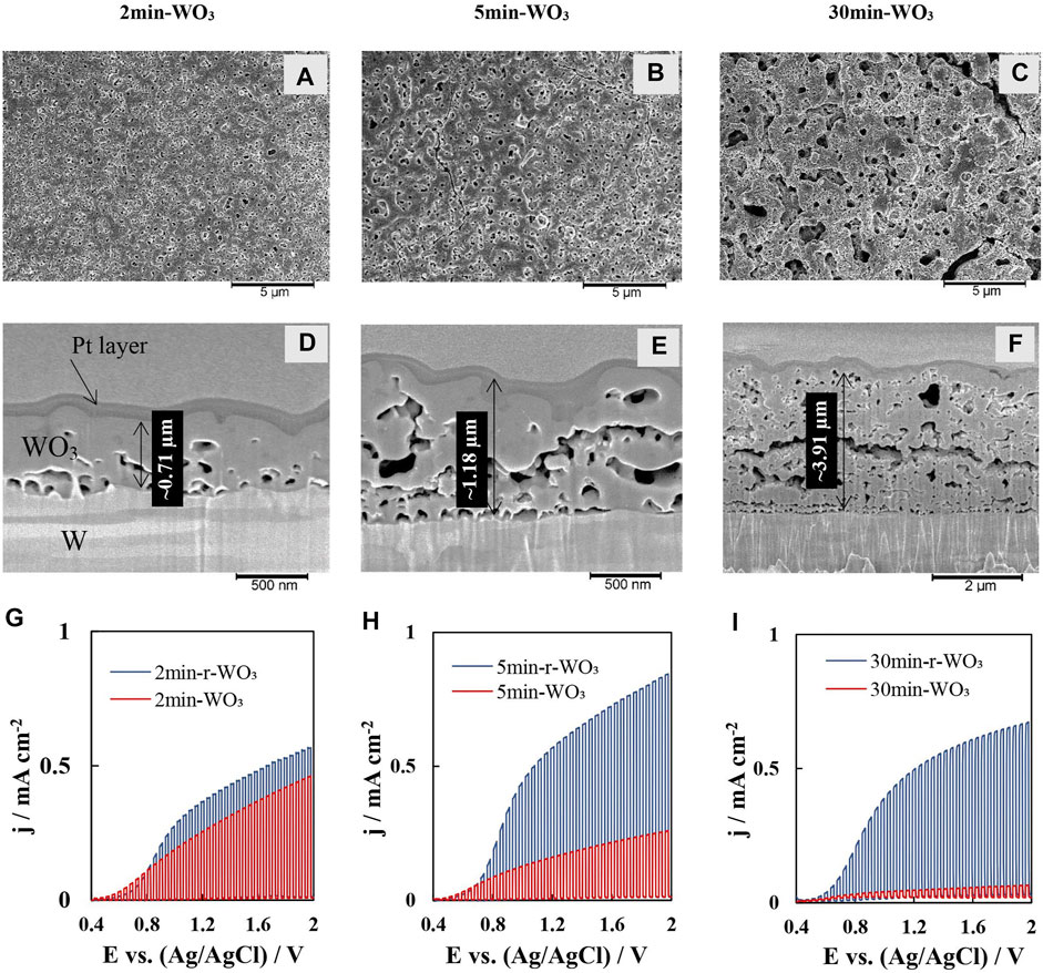
FIGURE 1. SEM images of as-anodized WO3 films: top view (A–C) and FIB cross-sections (D–F); and chopped UV on/off linear sweep voltammetry scans (10 s ON / 10 s OFF at 2 mV s−1) of WO3 and r-WO3 films at I0 = 50 mW cm−2 (G–I).
The preliminary experiment performed on the WO3 films was linear sweep voltammetry with a chopped on/off UV illumination pulse. The potential (E) was scanned from 0.4 V up to a cut-off condition of 2 V at 2 mV s−1 (Figure 1G–I). At the onset near OCP only a small photocurrent (jph) up to ∼10 μA cm−2 was observed for all films, but afterwards jph rapidly grew with increasing applied potential. Here the background current (which can be inferred from the “UV off” parts of the polarization curves) was not corrected for, but it was on the level of a few μA cm−2 throughout the experimental potential range, so the entire measured current is attributed to photocurrent. This relation between jph – E is expected, because as the strength of the electric field is increased, the space-charge layer within the semiconductor also broadens, which allows more photogenerated charge carriers to participate in the circuit. Note, that the r-WO3 LSV curves shown here were registered after a 3,000 s equilibration step, during which the re-oxidation current settled at a near-zero value.
The jph may be expected to plateau when either: 1) the space charge layer becomes of similar dimension as the penetration depth of incident light, or 2) diffusion limitations begin hindering charge transfer. This phenomenon does not occur at least until 2.0 V showing that the films have a rather large operating potential range. LSV measurements demonstrate that thinner (2min- and 5 min-WO3) films generate the highest photocurrents. In contrast, the longest anodization time (thickest film) yields a photoanode with very poor photocatalytic properties (Figure 1G–I red lines). The highly disordered structure of thicker films is not conducive to efficient charge transfer, and this reflects in the relatively poor photocatalytic activity of this film. Namely, 30min-WO3 has a maximum jph = 0.045 mA cm−2, while 2min-WO3 films produce a maximum jph = 0.46 mA cm−2.
An inverse effect was observed for r-WO3 films (Figure 1G–I blue lines). The electrochemical reduction and activation treatment increased the photocatalytic activity of the 30min-r-WO3 film over 10 times, whereas the 2min-r-WO3 film showed only a marginal improvement versus its as-anodized counterpart. After reduction water permeates into the film and protons intercalate into the near-surface WO3, forming a HxWO3 hydrogen tungsten bronze (Reichman and Bard, 1979). This structure has been reported to be significantly more conductive than WO3 (Whittingham, 2004; Xi et al., 2014). As the structure becomes more conductive photogenerated electrons reach the back contact faster; this results in faster photogenerated charge transfer kinetics in LSV and steady-state measurements. It is also likely that reduction decreases the number of defects that act as electron or hole traps in this material, thus increasing photon conversion efficiency (Liu et al., 2016). Both of these effects result in a much higher measured photocurrent for r-WO3 films. The overall highest photocurrent was generated by the 5min-r-WO3 film.
The potentiostatic curves that were obtained at 1.2 V in Figure 2A show the behavior of measured current under constant illumination. A near-steady-state photocurrent for as-anodized WO3 films is reached almost immediately, with the exception of 2min-WO3, which reaches a maximum current after ∼ 30 min. In contrast, for the reduced films the initial current decreases sharply until a minimum is reached after 60 – 300 s based on anodization time. Then the measured current densities begin to increase and only approach steady state after ∼ 2 h.
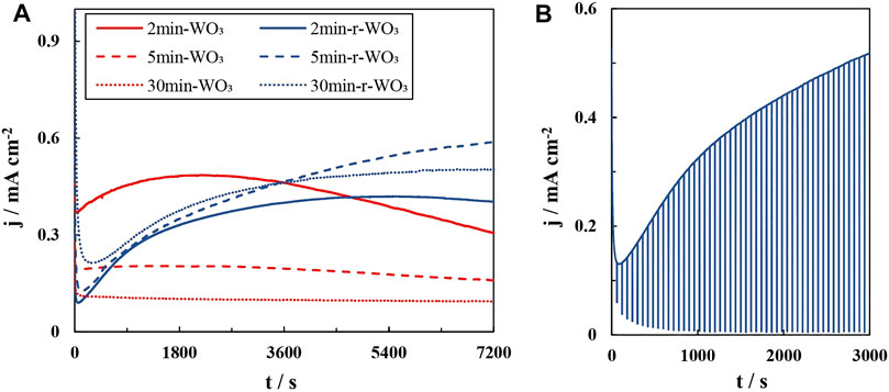
FIGURE 2. Potentiostatic steady-state photocurrent curves of WO3 and r-WO3 films (A); activation process of a 5min-r-WO3 film (B). Both dependencies were obtained at 1.2 V and I0 = 50 mA cm−2.
The anodic activation after the reduction step was performed because it had been noticed that it takes some time of potentiostatic illumination for the r-WO3 films to approach a steady-state photocurrent. In the curves of Figure 2A the background current was neglected. To illustrate the simultaneously occurring “dark” process, Figure 2B presents a typical activation curve obtained for a 5min-r-WO3 film at 1.2 V. Here constant illumination was interrupted by switching the LED off for 2 s every 60 s. Thus the “UV off” parts of the curve reasonably represent the dark current. As the measurement begins the dark current starts at ∼ 60 μA cm−2 and drops to fewer than 10 μA cm−2 after 1,000 s. In contrast, jph (the difference between the UV off and UV on pulses) increases from ∼0.12 mA cm−2 to 0.5 mA cm−2 (Figure 2B). It is assumed that the increase in photocurrent during activation of reduced WO3 films is not linked to background processes such as re-oxidation, which is attested by XPS analysis discussed below.
Potentiostatic UV on/off pulses at 1.2 V were applied in order to obtain information on jt=0 (the instantaneous photocurrent) and jss (the steady-state photocurrent). The most rudimentary interpretation of a photocurrent pulse profile is that the difference between jt=0 and jss is proportional to the amount of minority charge carriers that recombine at the semiconductor’s surface, i.e., transfer efficiency (Mokhtarimehr and Tatarkova, 2017). It is, however, evident that only the 2min-WO3 (Figure 3A) and 2min-r-WO3 (Figure 3B) films exhibit the initial “overshoot”. Even in this case jss is approached rapidly, and the difference can be effectively disregarded. The transfer and recombination kinetics will be further elucidated using non-stationary photoelectrochemical methods in Intensity Modulated Photocurrent Spectroscopy Study Section. The slight decrease of jph over the duration of the pulse also shows that the 2min-WO3 and 2min-r-WO3 films are less photoelectrochemically stable. This could be caused by non-reversible electron-hole recombination and the depletion of the space charge layer, but it could also be related to electro- or photo-corrosion of the films under anodic conditions.
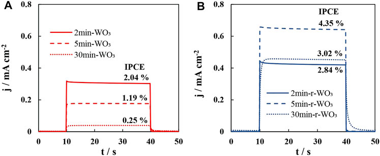
FIGURE 3. Steady-state potentiostatic on/off photocurrent pulses of WO3 films obtained after anodization at 25 mA cm−2 for the indicated amount of time: as-anodized (A); reduced and activated (B). All dependencies were obtained at 1.2 V and I0 = 50 mA cm−2.
To investigate whether any structural changes occur in the material during reduction and activation, XPS spectra were registered for 5min-WO3 films: as-anodized, just after reduction, and after reduction followed by an activation step as shown in Figure 2B. The W4f core-level spectrum of an as-anodized film consists of two peaks at 38.1 and 36.0 eV (Figure 4A). These peaks are fitted well by a doublet that corresponds to W6+ oxide [4f5/2 ∼ 37.8 eV, 4f7/2 ∼ 35.7 eV (Blackman and Parkin, 2005; Yang et al., 2009; Li et al., 2010)], although a small shift towards higher binding energies is seen. Peak integration shows that 96.9% of the area belongs to the W6+ signal (Table 2). Fitting also reveals a small amount (3.1 %) of W5+ (4f5/2 37.3 eV, 4f7/2 35. eV / Δ B.E. 2.1 eV), for which similar binding energies were reported (Wang et al., 2012; Hu et al., 2021). It is possible for W5+ to exist in the structure as a residual intermediate W2O5 left after anodization, but more likely this signal occurs due to the appearance of defect sites – oxygen-deficient W within the crystal lattice (Cheng et al., 2013). WO3 is an n-type semiconductor where oxygen vacancies act as electron donor sites, and at the semiconductor/electrolyte interface exposed W5+ sites adsorb oxygen species and participate in the OER mechanism as active sites. Moreover, in the O1s spectrum (Figure 4B) the peak at 531 eV deconvolutes into three binding states that have been attributed to O-W bonds (530.8 eV), O-vacancies (531.4 eV), and O-OH bonds (532.4 eV) (Vasilopoulou et al., 2014; Yu et al., 2017; Lee et al., 2018).
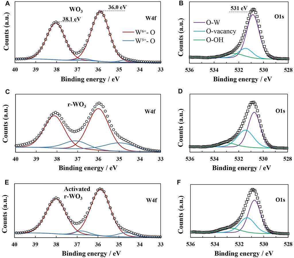
FIGURE 4. High-resolution W4f and O1s XPS spectra and fitted peaks of 5min-WO3 films: as-deposited (A, B); after reduction at -0.5 V for 300 s (C, D); after reduction and activation at 1.2 V, I0 = 50 mW cm−2, 3,000 s. (E, F).
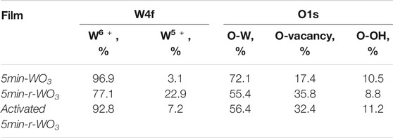
TABLE 2. Ratios of W and O bonds in as-anodized and modified WO3 films, obtained from integration of XPS peak areas.
It is therefore all the more intriguing that after reduction the signal of W5+ grows substantially (Figure 4C). 18.3% of the peak area can now be attributed to W5+ bonds and the signal of W6+ decreases correspondingly. Analysis of the respective O1s spectrum reveals a drop in O-W bonds (from 72.1 % before reduction to 55.4% after), and a double increase of the O-vacancy bond signal. Also, the O-OH signal had decreased, suggesting that the intercalated protons interact with exposed unsaturated W rather than O at the semiconductor/electrolyte interface. It has been suggested that electrochemical reduction of WO3 results in the formation of tungsten bronzes with an approximate stoichiometry of HxWO3, and the results of this measurement agree with that.
Steady-state measurements showed that immediately after reduction the r-WO3 films are poorly photoactive, but after an activation step, they typically generate several times larger photocurrents. Figure 4D shows the W4f spectrum of an activated r-WO3 film: it appears as an intermediate between plain WO3 and fresh r-WO3. The signal of W5+ had decreased, but the integrated peak area was still 7.1% - over two times larger than for the WO3 film. However, although the amount of W6+ had returned to near-initial levels, the O-vacancy signal remained elevated even after activation. This correlation between structure and photoactivity may be related to the emergence of an optimal amount of W5+ sites/oxygen vacancies. Too few vacancies (e.g., for plain WO3) reduce the effect of them acting as electron donor dopants overall, resulting in poorer photoexcitation of charge carriers. Too many vacancies (as for fresh r-WO3) act as electron traps, and promote recombination of photogenerated charge carriers. Then the mechanism of activation may be such: when a fresh r-WO3 film is illuminated, photogeneration and transfer of charge carriers begins. Recombination inevitably occurs due to the increased number of W5+ trap sites, and the observed jph is relatively small. Over time, as this process proceeds, non-reversible recombination results in the decrease of the number of trap sites – this results in a larger jph, and corresponds to a weaker W5+ signal in the XPS spectrum of an activated film. A small increase of the Na 1s signal was also observed after activation (0.18–0.55%), which may be a sign of anodic intercalation that has been documented to occur on bulk WO3 (Szkoda et al., 2021). Therefore, electrochemical reduction, followed by activation, can possibly be used to quite accurately tune the number of vacancies in WO3 films.
Electrochemical impedance spectra were obtained with a constant light intensity of 50 mW cm−2 at increasingly anodic applied potentials (0.4, 0.8, 1.2, 1.6, 2.0 V). A good understanding of the system under investigation is crucial for interpretation of impedance spectra. It is evident from polarization data (Figure 1) that under dark conditions no Faradaic processes occur on WO3 films, and the same is assumed for the reduced and activated films. This means that charge carrier photoexcitation within the space charge layer will decide the low frequency response of the PEIS spectra of this system.
A collection of representative PEIS spectra is presented in Figure 5. From the Nyquist coordinates it is apparent that the WO3 impedance response draws a depressed semicircle in the complex plane. The width of this semicircle is smallest for the most photoactive films (i.e., 2min-WO3), and the magnitude of the film’s impedance increases with anodization time. Although the complex plane seems to display one semicircle, a closer look at the Bode coordinates reveals that the response is in fact comprised from two distinct time constants (Figure 5B), which are only well distinguishable for 5min-WO3 and 30min-WO3 films. Only the low-frequency component could be extracted for the 2min-WO3 film.
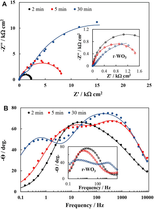
FIGURE 5. PEIS spectra obtained at I0 = 50 mW cm−2and 1.2 V in Nyquist (A) and Bode phase (B) coordinates of WO3 and r-WO3 (insets) films that have been formed by anodizing for 2, 5, and 30 min. Solid lines show fits to the equivalent circuit in the inset of Figure 6.
The electrochemical reduction and activation process seems to work by increasing the conductivity of the films, as is confirmed by their PEIS spectra (Figures 5A,B insets). The impedance magnitudes of r-WO3 decrease several times when compared to their respective as-anodized films.
As was the case with jph measurements, the effect is most significant for the least-photoactive 30min-WO3 film. It is also interesting to note that from the Bode spectra it appears that, while reduction has little effect on the low frequency range, it strongly suppresses the high frequency response. In PEIS high frequencies can often be attributed to capacitances caused by the charge/discharge of the double layer and intermediate surface states. This may be an indication that the r-WO3 material has more favorable adsorption/desorption kinetics of OER intermediates because the high frequency response is more in phase with the perturbation. In a typical full characterization of a film the PEIS spectra were registered at incrementally increasing anodic potentials up to 2.0 V. LSV measurements had shown that in this range jph grows with applied potential, but interestingly the system’s impedance also increases (Figure 6). This means that the semiconductor material becomes less conductive even though a higher generated photocurrent is observed. Technically, this behavior can be related to the jph – E curves that can be inferred from the “UV On” parts of Figure 1.
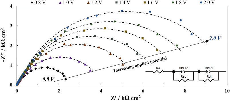
FIGURE 6. PEIS spectra of 5min-WO3 film in dependence on the anodic potential. Inset: the equivalent circuit that was used for fitting.
A sharper rise in jph is observed at lower potentials, and the increase trends toward a plateau as the potential is further swept anodically. Because the PEIS response is generated by integrating a small part of the jph – E curve under perturbation by a set potential amplitude, a steeper curve will result in more integrated current – a smaller impedance. These considerations can be further elaborated by applying equivalent circuit fitting.
The measured spectra were processed by fitting them to an equivalent electrical circuit (EC), where a single time constant is represented by an RC element with a capacitor connected in parallel to a resistor. Because two time constants are generally observed, the EC must have two RC elements. This results in an EC that is commonly used in electrochemical impedance modeling, and has been frequently applied to fit the spectra of photoanodes (Figure 6 inset).
In this circuit Rs is the series resistance. CPEdl is the double layer (Helmholtz) capacitance represented by a constant phase element to account for surface inhomogeneity, but it can overlap with a capacitance that is caused by the charge/discharge of surface states. Rct is the associated charge transfer resistance. CPEsc and Rsc are related to the semiconductor’s space charge layer: CPEsc should be proportional to the layer’s width, provided that the depletion zone acts as an insulating layer. The nature of Rsc requires a deeper explanation. Broadly speaking, a resistance is a measure of the electrical force that a charge carrier must overcome in order to move through an electrical field of certain strength. Rsc may be thought of as the electrical resistance of the space charge layer between the point where a charge carrier is generated and where it exits the layer. When the photoanode is illuminated, a flux of holes (that is equal to the flux of incident photons multiplied by a conversion coefficient) begins moving in the direction of the semiconductor/electrolyte interface. Therefore, Rsc must be a measure of this flux. The circuit’s parameters were plotted as a function of applied potential, and these trends were then compared to examine whether the increased photoactivity of r-WO3 over plain films could be attributed to any of them. The results of an exemplary analysis are presented in Figure 7.
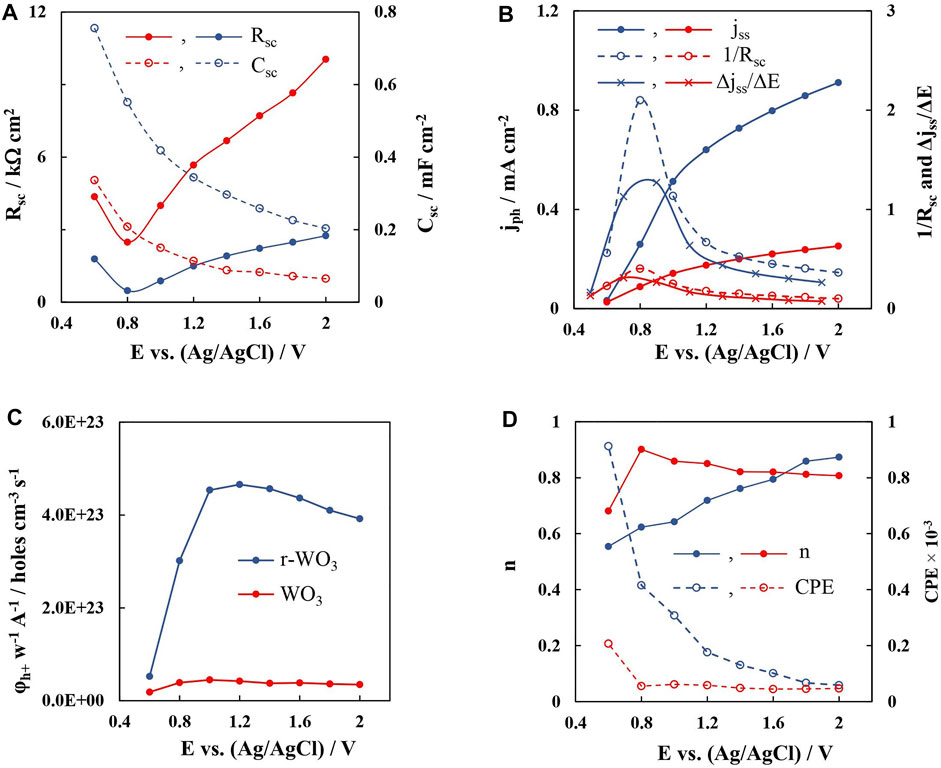
FIGURE 7. Results of the EIS fitting data for WO3 (red lines) and r-WO3 (blue lines) presented as trends over applied potential: the low frequency components Csc and Rsc (A); steady state photocurrent and modeled Rsc (B); the calculated charge carrier density (C); the high frequency constant phase element components CPEdl and n (D). Data are for 5 min (A–C) and 30 min. (D) films.
Interesting tendencies are revealed when examining the space-charge-related components and their relation to the applied potential (Figure 7A). The physical meaning of Csc can be likened to the width of the space charge layer within an illuminated photoactive semiconductor. As the photogenerated charge carriers transfer away (e- towards the back contact, and h+ towards the electrolyte) an insulating depletion region forms, resulting in a measurable capacitance. As the depletion layer widens, the capacitance should decrease. The Csc values for both WO3 and reduced films decrease with applied potential, but generally Csc of r-WO3 films are larger, indicating smaller space charge layer widths. It must be pointed out that this interpretation assumes that the relative permittivity of the material remains constant, which may make the comparison less accurate.
On the other hand, Rsc values increase linearly with applied potential, reflecting the growing magnitude of the spectra in Figure 6. This is a peculiar observation, as it implies that the system is becoming less conductive while the steady-state photocurrent increases (Figure 7B). 1/Rsc, which should be in some way representative of photogenerated charge carrier transfer, drops with applied potential in stark contrast with the increasing steady-state photocurrent. If the incident photon flux is constant, and bias potential is increased (i.e., the space charge layer expands), the photogenerated charge carrier flux should also increase. All this points towards that Rsc is not a direct measure of the flux. Instead, it is related to the change of the flux over bias potential – Δφh+/ΔE. Values of jss that had been obtained from steady state UV pulse measurements were used to calculate the rudimentary derivative values of Δjss/ΔE, which are presented as a function of applied potential in Figure 7B. It can be seen that, although experimental errors could have distorted the results, the same decreasing trend is observed. Moreover, this relation between the charge carrier flux and applied electric field strength is effectively photoconductivity as measured in mA V−1 cm−2. It then follows that this decrease in photoconductivity is what determines the Rsc parameter.
The physical cause of this phenomenon can be traced to the balance between the expanding space charge layer and decreasing charge carrier density. If Csc can be considered a reasonable approximation of the capacitance of the space charge layer, then its width W should be proportional to 1/Csc as per the parallel plate capacitor equation. If the relative permittivity εr were to be known, the width of the depletion zone could be calculated. The εr of WO3 is known to vary based on electrodeposition conditions, but for illustration purposes a value of 33.3 (obtained for WO3 films formed by anodization in 0.3 M oxalic acid (Levinas et al., 2017)) will be considered. Then the width and volume of the space charge layer is calculated, and the values of charge carrier density are presented as a function of applied potential in Figure 7C. It is evident that the charge carrier density reaches a peak at a certain potential, which is ∼ 1 V for the WO3 film but closer to 1.2 V for r-WO3. After this, the charge carrier density begins to decrease linearly as the space charge layer continues to expand. It is also worth noting that this peak almost exactly corresponds to where the observed steady state photocurrents intersect the calculated 1/Rsc trends in Figure 7B. It may then be concluded that the steady state photocurrent is equal to the photoconductivity when the hole density within the space charge layer is at a maximum. Functionally, jph continues to rise with further increasing potential, as its magnitude depends on the minority charge carrier flux rather than conductivity.
The origins and behavior of the high frequency components are more complicated to interpret. Cdl should be caused by the charge and discharge of the Helmholtz double layer that forms at the semiconductor/solution interface, so it is proportional to the electrochemically active surface area of the electrode. However, it is sometimes noticed that in PEIS the Helmholtz capacitance is mixed with a capacitance that arises from the dynamic surface charging by intermediate states (Fermín et al., 1999). In Figure 7D instead of recalculating CPE values capacitance they are presented as-modeled, along with the n exponent of the CPE element. The values of CPE for WO3 films are low and n drops from 0.9 to 0.8 over the measured potential range, but for r-WO3 n values begin at ∼ 0.55 and rise linearly to 0.87. This behavior seems to imply that on r-WO3 films some surface diffusion of intermediate states may occur at lower potentials. Moreover, the values of Rct of the reduced film were up to 40 times lower than those of the plain film.
IMPS was used to complement PEIS results, as it provides additional information on photon conversion efficiency and hole transfer kinetics. The classic theory has been elucidated by Ponomarev and Peter in their seminal work (Ponomarev and Peter, 1995), and textbook applications have been excellently explained in multiple publications (Fermín et al., 1999; Klotz et al., 2016; Zachäus et al., 2017; Antuch et al., 2018; Amano and Koga, 2020; Rodríguez-Gutiérrez et al., 2020) which were taken into consideration when interpreting the obtained spectra. Initially, measurements were carried out at 1.2 V and increasing light intensities (I0: 10–60 mW cm−2 at increments of 10 mW cm−2). Under potentiostatic conditions the width of the space charge layer should remain constant, as it is mostly dependent on the bias potential. According to the Gärtner equation (Gärtner, 1959) then the increase in jph should be related to the flux of photogenerated charge carries within the space charge layer, which is equal to the incident photon flux multiplied by a conversion coefficient.
The IMPS spectra shown in Figure 8 exhibit some unique characteristics. For one, the spectra begin in the third quadrant of the complex coordinate plane. This is an experimental fact that has also been observed for Fe, Ti, and W oxides (Peat and Peter, 1987; Goossens, 1996; Rodríguez-Pérez et al., 2017), and its origin is the high-frequency charge/discharge of the double layer. For this reason, the high frequency time constant is often called the “cell” time constant, and it is the product of solution resistance and total cell capacitance (τs = Rs*Ctot). All of the spectra then intercept the H″ axis at 417 Hz (at which the phase shift equals -90°), after which substantial low frequency semicircles begin. It is immediately apparent that there is no surface recombination at this applied potential – at low frequencies the spectra trend towards intercept with the H′ axis as the phase nears 0. According to IMPS theory, the low frequency semicircle is expected to reach a maximum at a certain frequency which is equal to the sum of both transfer constants (ωLF = ktr + krec). If no recombination is experimentally observed, then ktr >> krec, and ωLF = ktr (Ravishankar et al., 2019). That is to say, the entire IMPS response, comprised from two semicircles, will be confined to the fourth quadrant of the complex coordinate plane. This is almost exactly what is observed in the obtained spectra – the low frequency semicircle decreases in magnitude with increasing I0, while the high frequency response is not significantly altered by light intensity.

FIGURE 8. IMPS spectra obtained at 1.2 V in dependence on UV light intensities (10% modulation amplitude). Measured on 5min-r-WO3 film. Dashed lines represent semicircle fits.
However, although they appear as semicircles, they could not be modeled with a single CPE element, likely due to interference from the high-frequency response. In order to better distinguish the signal that occurs due to hole transfer, the following procedure for processing IMPS spectra was adopted: a semicircular fitting with a simple R1(CPE-R2) equivalent circuit was applied to the low-frequency response. From the obtained values an entire semicircle was simulated on the complex plane plot. The values of ?LF and H'ω→0 were obtained from this simulated semicircle that corresponds to the low frequency response. Note that here the parameters of the equivalent circuit do not have a physical meaning as they would in EIS. These observations point to the conclusion that, much like in electrochemical impedance spectroscopy, if two time constants are different by enough magnitudes, non-stationary spectroscopy methods will allow the discernment of one or both of them. In this case τs is impossible to calculate, but tLF is. The validity of this approach is shown in Figure 9 by comparing various parameters that had been obtained from steady-state, PEIS, and IMPS experiments.
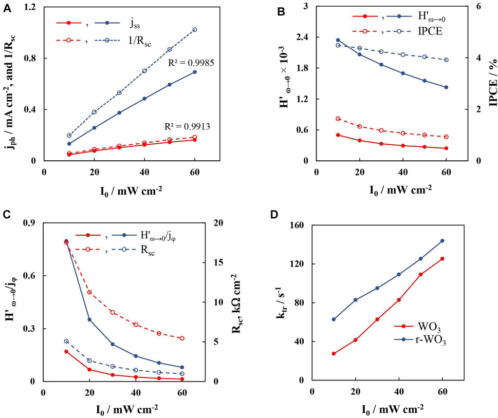
FIGURE 9. Analysis data of the IMPS spectra for WO3 (red lines) and r-WO3 (blue lines) in dependence on applied illumination intensity: steady-state photocurrent and Rsc−1 (A); trends of the low frequency intercept with the real axis and IPCE (B); trends of the normalized low frequency intercept and Rsc, obtained from PEIS data (C); transfer constants, obtained from IMPS (D). Data measured for 5min films, at 1.2 V.
The steady-state photocurrent increases linearly with I0 for both WO3 and r-WO3 films (Figure 9A). This is the first indication as to the mechanism of water oxidation: it has been demonstrated that this behavior is related to whether the photoelectrochemical reaction occurs through direct or indirect (i.e., hydroxyl radical assisted) hole transfer (Villarreal et al., 2004; Mora-Seró et al., 2005). In this case, a linear relation of jph to the light intensity is an indication of direct hole transfer. From parallel PEIS experiments it was determined that at 1.2 V for a WO3 film, 1/Rsc values are almost equal to the observed steady state photocurrent. Conversely, for the reduced electrode, 1/Rsc values were larger throughout (also as seen in Figure 7B).
As was discussed earlier, Rsc is a measure of the semiconductor’s conductivity owing to the photogenerated charge carrier flux. The potentiostatic mode keeps the strength of the electric field effectively constant, and therefore the changes in the charge carrier flux are directly related to the increasing incident photon flux, as per the Gärtner equation. As the hole flux increases at a constant potential, the conductivity and 1/Rsc is observed to grow linearly with I0. The difference between jph and 1/Rsc then becomes even more remarkable: for the WO3 films - a collected e− results in one h+ joining the flux because jph ≈ 1/Rsc, but for the r-WO3 films a collected e− yields ∼ 1.41–1.49 h+ based on I0.
The second important parameter of IMPS spectra is the low-frequency intercept with the real axis. The real axis of an IMPS plot is fundamentally related to quantum efficiency, i.e., the ratio between the photogenerated current and the incident photon flux. The so-called external quantum efficiency (EQE, functionally identical to IPCE) is defined as:
Here je is the collected electrical current, and jφ is the spectral flux expressed in the units of current, q is the elementary charge. If an IMPS spectrum were to be normalized by assuming that the maximum observed value of the real axis H’ equals 1, then the low frequency intercept with the real axis would give the transfer efficiency. However, if the spectrum were to be normalized by the incident photon flux or not normalized at all, then the low frequency intercept should be proportional to the EQE.
At low frequencies the collected current approaches steady state, thus, the low frequency intercept should be proportional to the IPCE values that were calculated from steady-state photocurrent measurements. Indeed, for the non-normalized H spectra that were presented in Figure 8, it is observed that H’ω→0 values decrease with I0 with the similar tendency as for IPCE (Figure 9B). However, these values are dimensionless and demonstrably cannot be equated to steady state photocurrent. Here the enhanced photon conversion efficiency of r-WO3 films is again seen, as the intercept values of the reduced film are ∼ 5 times larger than those of the WO3 film.
Another observation was made when normalizing the presented H’ω→0 values by jφ. The normalized H’ω→0 / jφ values decreased by a power law that was not entirely proportional to IPCE (Figure 9C). In fact, the only other parameter within the system that would exhibit such a trend with I0 was Rsc, obtained from parallel PEIS measurements under identical conditions. Of course, if H’ω→0 ∼ jss. / jφ, then H’ω→0 / jφ will be proportional to 1/jss (which is directly related to Rsc as discussed earlier). These results are interesting, and they connect the various parameters obtained by PEIS and IMPS. In practice this means that while the low frequency intercept is proportional to conversion efficiency, the normalized intercept is more proportional to photoconductivity.
Finally, the transfer constants of both plain and reduced films were found to increase with I0 in linear trends (Figure 9D). The ktr of the WO3 film ranged from 27.3 s−1 to 125.3 s−1, whereas for the r-WO3 film it was almost double at lower intensities from 62.8 s−1 to 143.8 s−1. Thus, the conductivity of the reduced films is larger, and the injection of holes into the electrolyte occurs at a faster rate, resulting in overall enhanced photocatalytic water splitting properties.
The following conclusions have been made about applying IMPS analysis to these films: photocatalytic activity in terms of steady-state photocurrent is directly proportional to 1/Rsc that is obtainable by equivalent circuit fitting of PEIS spectra. Also, the low-frequency intercept H'ω→0 is proportional to EQE, and larger H′ values correspond to enhanced photon conversion efficiencies. Further implementation of this analysis is shown in Figure 10A. Here, the presented spectra had been obtained at different bias potentials. A significant difference is observed for the low frequency intercept H'ω→0 – its values increase as the applied potential is raised towards more anodic values. Recalling the previous discussion, this must mean that better photon conversion efficiency is achieved at higher potentials. Conversely, ?LF decreases, which is not apparent from the profile of the spectra, but will be discussed in more detail later on.
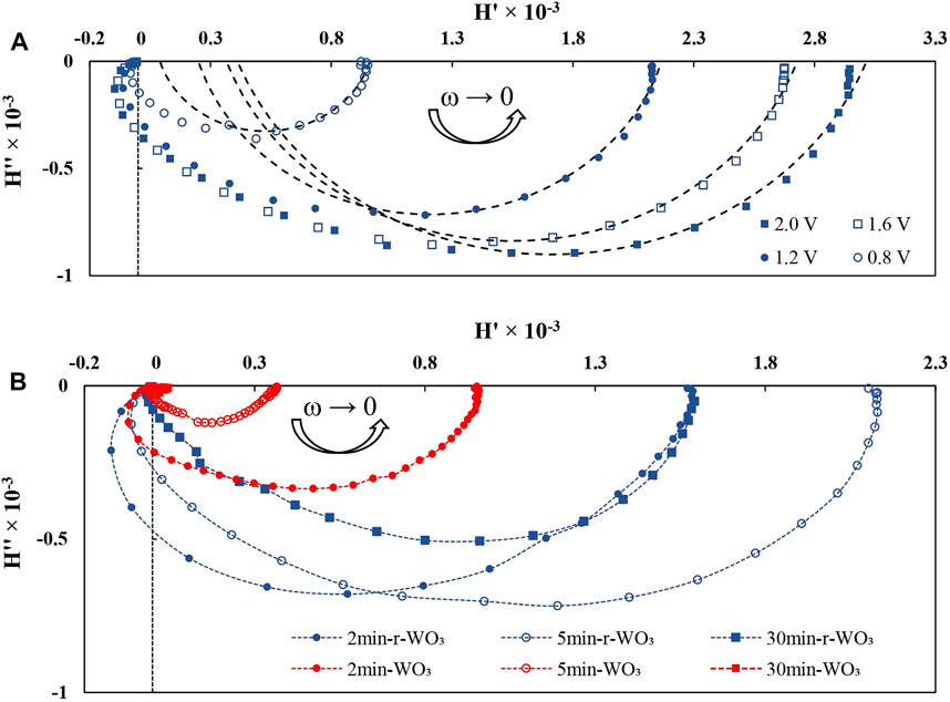
FIGURE 10. IMPS spectra obtained at I0 = 50 mW cm−2 and 1.2 V in dependence on: applied potential for 5min-r-WO3 films (A); anodization time for WO3 and r-WO3 films (B).
The IMPS spectra (obtained at 1.2 V) of films that had been formed by anodization for increasing times are particularly intriguing, and are presented in Figure 10B, but without fitting. For the films that had been formed by shorter anodizing durations (2, 5 min) the high frequency response overlaps the low frequency signal, as a broad semicircle is observed in the first half of the spectrum. This complicates estimation of ?LF, but modeling by simulation and extrapolation of the low frequency response yielded usable data in most cases. Designation of the low frequency extremum is a known issue in IMPS analysis, and this method may result in an over- or under-approximation, but it provides consistency of data acquisition.
Furthermore, these films may also exhibit some recombination as is signaled by the appearance of a trend toward low frequency semicircles in the first quadrant, but these recombination signals are negligible and have been disregarded from broader data analysis. The low frequency intercepts with the real axis show that 2min-WO3 and 5min-WO3 films reach better photon conversion efficiencies, which fall drastically when the anodization time is extended to 30 min. As expected, the r-WO3 films have larger low frequency intercept values owing to their enhanced conversion efficiencies.
The relation between applied potential and transfer kinetics/conversion efficiency must also be discussed. IMPS analysis shows that as bias potential is increased the photon conversion efficiency also increases, which is in agreement with steady state measurements. To illustrate these tendencies, as well as to compare WO3 and r-WO3 films, Figure 11 contains the values of low frequency intercepts with the real axis, as well as transfer rate constant values that were obtained directly from ωlf. It is seen that H'ω→0 increase with applied potential, and the intercept values of reduced films are overall larger, showing better photon conversion efficiency and directly relating to the observed difference in steady state photocurrents. In contrast, here the transfer rate constants ktr of the reduced film are smaller than that of the plain WO3 film. Moreover, ktr decrease steadily throughout the entire potential range. It has been suggested that this behavior can be related to the mechanism of oxygen evolution through either mobile or immobile intermediate surface states (Kandiel, 2020). If ktr increases with applied potential it would suggest that oxygen evolution occurs through coupling of two adjacent oxygen-containing intermediates. Otherwise, the trend of ktr would point towards a mechanism where oxygen evolution occurs through a single immobile active site which reacts with other photogenerated holes and adsorbed OH− species. Then ktr, obtained from IMPS, may be related to jph – I0 measurements (as in Figure 9A), which also give an indication as to whether hole transfer proceeds through indirect (mobile) or direct (immobile) steps. In this case the ktr – E and jph – I0 behavior of the films agree and strongly suggest that water oxidation proceeds through direct hole transfer.
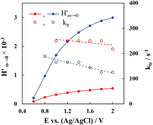
FIGURE 11. Low frequency intercepts and transfer rate constants as a function of applied potential for 5min-WO3 (red curves) and 5min-r-WO3 (blue curves) films.
Typically, when a WO3 film is illuminated an instantaneous flux of photogenerated holes moves toward the semiconductor/electrolyte interface. If there is surface recombination, then jt=0 will be larger than jss (0 < jt=0/jss < 1), and a characteristic “overshoot” will be observed. In an ideal case, jt=0 would equal jss, meaning all holes that arrive at the interface are transferred into the electrolyte. Finally, it is also possible that jt=0 be smaller than jss, as was observed for the 30min-WO3 film (Figure 12 and insets). Upon illumination the measured photocurrent grows slowly until the flux of electrons arriving at the back contact reaches a maximum, and a small but distinguishable jss peak is seen in steady-state curves. For the plain WO3 film 0.04 mA cm−2 was reached within ∼ 10 s of illumination. This is obviously a negative characteristic, as it is indicative of slow charge transfer, poor charge carrier separation, and short lifetime of photogenerated holes. However, it presents an excellent opportunity to elucidate the effects of reduction on the photocatalytic properties of anodized WO3 films.
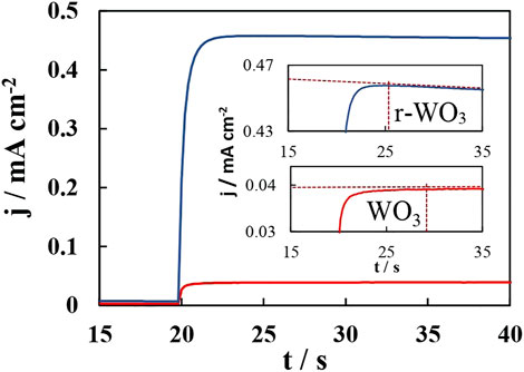
FIGURE 12. Photocurrent transients measured at 1.2 V and I0 = 50 mW cm−2 for 30min-WO3 (red curve) and 30min-r-WO3 (blue curve) films. Insets show close-up views of the initial moments of the light pulse.
After reduction two substantial changes are seen: the maximum photocurrent is reached faster, in up to 5 s, and it becomes ∼10 times higher (0.46 mA cm−2). As it was discussed earlier, the morphology of 30min-WO3 films is highly porous, which hinders charge transfer. Electrochemical reduction increases the permittivity of the film by forming a conductive HxWO3 phase throughout the porous structure on the surface that is exposed to the electrolyte. This explains faster charge transfer, but not a larger photocurrent, because a larger photocurrent must be related to photogenerated charge carrier generation or separation. Although, IMPS is usually used to discern low frequency near-surface recombination, the spectra of these films had certain characteristics that seem to indicate a signal inversion at high frequencies (Figure 13, spectra presented without fitting). In particular, for 30min-WO3 films the admittance modulus |H| declines to a minimum in the 10 – 1 kHz range (Figure 13A), and this coincides with a sign reversal of the phase (Figure 13B). In Nyquist plots this corresponded to the formation of a high frequency loop. The reduced film, however, had lost the phase inversion and |H| minimum. Also, these features were not observed for 5min-WO3 films: the admittance modulus rose steadily as the phase dropped to near 0.at 0.1 Hz.
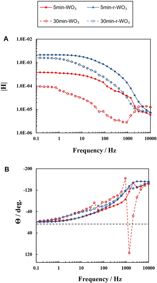
FIGURE 13. IMPS spectra obtained at I0 = 50 mW cm−2 and 1.2 V in Bode modulus (A) and Bode phase (B) coordinates for WO3 (red curves) and r-WO3 (blue curves) films.
It must be kept in mind that in IMPS the signal is related to photon conversion and not photocurrent. Then the drop in |H| must be indicative of decreasing conversion efficiency, which is most likely caused by recombination of photogenerated charge carriers with “traps” or defects. Because this is not low frequency recombination it occurs not near the semiconductor-electrolyte interface, but deeper within the bulk of the material, likely as electrons initiate diffusion toward the back contact during the initial stages of a light pulse. This can also be related to the steady-state photocurrents shown in Figure 12, where it takes 10 s for the photogenerated charge carrier flux of a WO3 film to approach steady-state due to their short life time. Because these features are absent from r-WO3 IMPS spectra, it can be concluded that reduction also decreased the amount of photogenerated charge carrier traps, and this results in a much higher photon conversion efficiency as can also be inferred from |H| values at near-steady-state. Furthermore, parallel PEIS measurements showed the Rsc of these films to be 11.44 kΩ cm2 (30min-WO3) and 3.485 kΩ cm2 (30min-r-WO3): a 3.3 time increase in conductivity after reduction, which corresponds well to the difference in charge transfer kinetics seen in steady-state pulses.
Therefore, IMPS spectra can be used as a qualitative indicator of bulk charge transfer efficiency – a decrease in admittance modulus and phase reversal seem to correspond to slow charge transfer kinetics due to the recombination with defects in the material’s structure.
Highly porous WO3 films have been obtained by galvanostatic anodization from the electrolyte containing F− and H2PO2−. The films were synthesized dependently on anodization time, which was varied up to 30 min. The FIB cross-sections revealed that their thickness increases with the anodization time, and all films have a porous morphology both on the surface and within the layer. XPS analysis showed that the as-anodized films are WO3, with a small W5+ signal. The photoelectrochemical performance for oxygen evolution assessed in an acidic Na2SO4 electrolyte, reveals that the shorter anodization times (2 or 5 min) yield films with rather high photocatalytic activity that could reach ∼ 2 % photon conversion efficiency at 1.2 V under 50 mW cm−2. However, the photocurrent of these films would drop considerably over a 2-h test period. Electrochemical reduction (H+ intercalation and activation) was applied on the as-synthesized WO3 films to overcome this drawback; this led to improved stability and activity. A maximum IPCE of 4.35 % was calculated for a reduced WO3 film that had been obtained after 5 min of anodization. XPS spectra reveal that after H+ intercalation the films show a stronger W5+-O and O-vacancy signal. However, after intercalation and activation, W5+ re-oxidizes, while the O-vacancy signal remains increased. PEIS and IMPS measurements confirmed that the photo-conductivity of r-WO3 was considerably superior, owing to more effective photoexcited charge carrier generation/separation. Finally, interpretation of the high frequency part of IMPS spectra suggests that reduction significantly reduces charge carrier recombination within the material’s bulk. Thus, an in-situ electrochemical reduction and activation treatment enhances almost every aspect of the photocatalyst – charge carrier photogeneration/separation, the kinetics of charge transfer, as well as rate of hole injection into the electrolyte. The proposed approach unlocks the catalytic activity towards OER of promising photoanodes.
The raw data supporting the conclusions of this article will be made available by the authors, without undue reservation.
The synthesis of the films, their SEM surface morphology and photoelectrochemical characterizations were performed by RL, under the supervision of NT and HC. The XPS structural characterization and modelling was performed by TM. Writing and original draft preparation by RL. Review and editing performed by RL, NT, and HC.
This project has received funding from the European Union’s Horizon 2020 research and innovation programme under the Marie Sklodowska-Curie grant agreement N° 778357- SMARTELECTRODES.
The authors declare that the research was conducted in the absence of any commercial or financial relationships that could be construed as a potential conflict of interest.
All claims expressed in this article are solely those of the authors and do not necessarily represent those of their affiliated organizations, or those of the publisher, the editors, and the reviewers. Any product that may be evaluated in this article, or claim that may be made by its manufacturer, is not guaranteed or endorsed by the publisher.
Ali, H., Ismail, N., Hegazy, A., and Mekewi, M. (2014). A Novel Photoelectrode from TiO2-WO3 Nanoarrays Grown on FTO for Solar Water Splitting. Electrochim. Acta 150, 314–319. doi:10.1016/j.electacta.2014.10.142
Amano, F., and Koga, S. (2020). Influence of Light Intensity on the Steady-State Kinetics in Tungsten Trioxide Particulate Photoanode Studied by Intensity-Modulated Photocurrent Spectroscopy. J. Electroanal. Chem. 860, 113891. doi:10.1016/j.jelechem.2020.113891
Antuch, M., Millet, P., Iwase, A., and Kudo, A. (2018). The Role of Surface States during Photocurrent Switching: Intensity Modulated Photocurrent Spectroscopy Analysis of BiVO4 Photoelectrodes. Appl. Catal. B: Environ. 237, 401–408. doi:10.1016/j.apcatb.2018.05.011
Bak, T., Nowotny, J., Rekas, M., and Sorrell, C. C. (2002). Photo-electrochemical Hydrogen Generation from Water Using Solar Energy. Materials-Related Aspects. Int. J. Hydrogen Energ. 27, 991–1022. doi:10.1016/S0360-3199(02)00022-8
Blackman, C. S., and Parkin, I. P. (2005). Atmospheric Pressure Chemical Vapor Deposition of Crystalline Monoclinic WO3 and WO3-X Thin Films from Reaction of WCl6 with O-Containing Solvents and Their Photochromic and Electrochromic Properties. Chem. Mater. 17, 1583–1590. doi:10.1021/cm0403816
Calero, S. J., Ortiz, P., Oñate, A. F., and Cortés, M. T. (2016). Effect of Proton Intercalation on Photo-Activity of WO3 Anodes for Water Splitting. Int. J. Hydrogen Energ. 41, 4922–4930. doi:10.1016/j.ijhydene.2015.12.155
Cao, J., Gao, Z., Wang, C., Muzammal, H. M., Wang, W., Gu, Q., et al. (2020). Morphology Evolution of the Anodized Tin Oxide Film during Early Formation Stages at Relatively High Constant Potential. Surf. Coat. Technol. 388, 125592. doi:10.1016/j.surfcoat.2020.125592
Casado, C., Mesones, S., Adán, C., and Marugán, J. (2019). Comparing Potentiostatic and Galvanostatic Anodization of Titanium Membranes for Hybrid Photocatalytic/microfiltration Processes. Appl. Catal. A: Gen. 578, 40–52. doi:10.1016/j.apcata.2019.03.024
Cheng, L., Hou, Y., Zhang, B., Yang, S., Guo, J. W., Wu, L., et al. (2013). Hydrogen-treated Commercial WO3 as an Efficient Electrocatalyst for Triiodide Reduction in Dye-Sensitized Solar Cells. Chem. Commun. 49, 5945. doi:10.1039/c3cc42206b
Chu, Y., Yu, G., Hu, B., Dong, Q., Zhang, J., and Zhang, X. (2014). Effect of Hypophosphite on Electrodeposition of Graphite@copper Powders. Adv. Powder Technol. 25, 477–482. doi:10.1016/j.apt.2013.07.003
Dong, C., Zhao, R., Yao, L., Ran, Y., Zhang, X., and Wang, Y. (2020). A Review on WO3 Based Gas Sensors: Morphology Control and Enhanced Sensing Properties. J. Alloys Compd. 820, 153194. doi:10.1016/j.jallcom.2019.153194
Fermín, D. J., Ponomarev, E. A., and Peter, L. M. (1999). A Kinetic Study of CdS Photocorrosion by Intensity Modulated Photocurrent and Photoelectrochemical Impedance Spectroscopy. J. Electroanal. Chem. 473, 192–203. doi:10.1016/S0022-0728(99)00109-6
Fernández-Domene, R. M., Sánchez-Tovar, R., Lucas-Granados, B., Roselló-Márquez, G., and García-Antón, J. (2017). A Simple Method to Fabricate High-Performance Nanostructured WO 3 Photocatalysts with Adjusted Morphology in the Presence of Complexing Agents. Mater. Des. 116, 160–170. doi:10.1016/j.matdes.2016.12.016
Gärtner, W. W. (1959). Depletion-Layer Photoeffects in Semiconductors. Phys. Rev. 116, 84–87. doi:10.1103/PhysRev.116.84
Gan, X., Zhou, K., Hu, W., and Zhang, D. (2012). Role of Additives in Electroless Copper Plating Using Hypophosphite as Reducing Agent. Surf. Coat. Technol. 206, 3405–3409. doi:10.1016/j.surfcoat.2012.02.006
Goossens, A. (1996). Intensity-modulated Photocurrent Spectroscopy of Thin Anodic Films on Titanium. Surf. Sci. 365, 662–671. doi:10.1016/0039-6028(96)00751-0
Gullapalli, S. K., Vemuri, R. S., and Ramana, C. V. (2010). Structural Transformation Induced Changes in the Optical Properties of Nanocrystalline Tungsten Oxide Thin Films. Appl. Phys. Lett. 96, 171903. doi:10.1063/1.3421540
Hu, Y., Hao, L., Zhang, Y., Ping, X., Liu, T., Zhao, Q., et al. (2021). Defect Concentration Regulation in Nanoflower-like WO3 Film and its Influence on Photocatalytic Activity. J. Mater. Sci. Mater. Electron. 32, 9412–9423. doi:10.1007/s10854-021-05605-2
Huang, Z.-F., Song, J., Pan, L., Zhang, X., Wang, L., and Zou, J.-J. (2015). Tungsten Oxides for Photocatalysis, Electrochemistry, and Phototherapy. Adv. Mater. 27, 5309–5327. doi:10.1002/adma.201501217
Kandiel, T. A. (2020). Mechanistic Investigation of Water Oxidation on Hematite Photoanodes Using Intensity-Modulated Photocurrent Spectroscopy. J. Photochem. Photobiol. A: Chem. 403, 112825. doi:10.1016/j.jphotochem.2020.112825
Karastoyanov, V., and Bojinov, M. (2008). Anodic Oxidation of Tungsten in Sulphuric Acid Solution-Influence of Hydrofluoric Acid Addition. Mater. Chem. Phys. 112, 702–710. doi:10.1016/j.matchemphys.2008.06.029
Klotz, D., Ellis, D. S., Dotan, H., and Rothschild, A. (2016). Empirical in Operando Analysis of the Charge Carrier Dynamics in Hematite Photoanodes by PEIS, IMPS and IMVS. Phys. Chem. Chem. Phys. 18, 23438–23457. doi:10.1039/C6CP04683E
Kwong, W. L., Savvides, N., and Sorrell, C. C. (2012). Electrodeposited Nanostructured WO3 Thin Films for Photoelectrochemical Applications. Electrochim. Acta 75, 371–380. doi:10.1016/j.electacta.2012.05.019
Lai, C. W., and Sreekantan, S. (2013). Fabrication of WO3 Nanostructures by Anodization Method for Visible-Light Driven Water Splitting and Photodegradation of Methyl orange. Mater. Sci. Semicond. Process. 16, 303–310. doi:10.1016/j.mssp.2012.10.007
Lee, S. Y., Shim, G., Park, J., and Seo, H. (2018). Tunable Polaron-Induced Coloration of Tungsten Oxide via a Multi-step Control of the Physicochemical Property for the Detection of Gaseous F. Phys. Chem. Chem. Phys. 20, 16932–16938. doi:10.1039/C8CP00158H
Levinas, R., Tsyntsaru, N., Lelis, M., and Cesiulis, H. (2017). Synthesis, Electrochemical Impedance Spectroscopy Study and Photoelectrochemical Behaviour of As-Deposited and Annealed WO 3 Films. Electrochim. Acta 225, 29–38. doi:10.1016/j.electacta.2016.12.112
Li, W., Li, J., Wang, X., Luo, S., Xiao, J., and Chen, Q. (2010). Visible Light Photoelectrochemical Responsiveness of Self-Organized Nanoporous WO3 Films. Electrochim. Acta 56, 620–625. doi:10.1016/j.electacta.2010.06.025
Li, Y., Tang, Z., Zhang, J., and Zhang, Z. (2017). Enhanced Photocatalytic Performance of Tungsten Oxide through Tuning Exposed Facets and Introducing Oxygen Vacancies. J. Alloys Compd. 708, 358–366. doi:10.1016/j.jallcom.2017.03.046
Lin, L., Cheng, C.-P., and Teng, T.-P. (2016). Electrodeposition-Based Fabrication and Characteristics of Tungsten Trioxide Thin Film. J. Nanomater. 2016, 1–12. doi:10.1155/2016/3623547
Liu, X., Wang, F., and Wang, Q. (2012). Nanostructure-based WO3 Photoanodes for Photoelectrochemical Water Splitting. Phys. Chem. Chem. Phys. 14, 7894. doi:10.1039/c2cp40976c
Liu, Y., Li, J., Li, W., He, H., Yang, Y., Li, Y., et al. (2016). Electrochemical Doping Induced In Situ Homo-Species for Enhanced Photoelectrochemical Performance on WO3 Nanoparticles Film Photoelectrodes. Electrochim. Acta 210, 251–260. doi:10.1016/j.electacta.2016.05.165
Macdonald, D. D., Biaggio, S. R., and Song, H. (1992). Steady‐State Passive Films: Interfacial Kinetic Effects and Diagnostic Criteria. J. Electrochem. Soc. 139, 170–177. doi:10.1149/1.2069165
Manovah David, T., Wilson, P., Ramesh, C., and Sagayaraj, P. (2014). A Comparative Study on the Morphological Features of Highly Ordered Titania Nanotube Arrays Prepared via Galvanostatic and Potentiostatic Modes. Curr. Appl. Phys. 14, 868–875. doi:10.1016/j.cap.2014.04.002
Mardare, C. C., and Hassel, A. W. (2019). Review on the Versatility of Tungsten Oxide Coatings. Phys. Status Solidi A. 216, 1900047. doi:10.1002/pssa.201900047
Mokhtarimehr, M., and Tatarkova, S. A. (2017). Photocurrent Transients of Thin-Film Solar Cells. J. Opt. Soc. Am. B 34, 1705. doi:10.1364/JOSAB.34.001705
Mora-Seró, I., Villarreal, T. L., Bisquert, J., Pitarch, Á., Gómez, R., and Salvador, P. (2005). Photoelectrochemical Behavior of Nanostructured TiO2 Thin-Film Electrodes in Contact with Aqueous Electrolytes Containing Dissolved Pollutants: A Model for Distinguishing between Direct and Indirect Interfacial Hole Transfer from Photocurrent Measurements. J. Phys. Chem. B 109, 3371–3380. doi:10.1021/jp045585o
Mukherjee, N., Paulose, M., Varghese, O. K., Mor, G. K., and Grimes, C. A. (2003). Fabrication of Nanoporous Tungsten Oxide by Galvanostatic Anodization. J. Mater. Res. 18, 2296–2299. doi:10.1557/JMR.2003.0321
Ou, J. Z., Balendhran, S., Field, M. R., McCulloch, D. G., Zoolfakar, A. S., Rani, R. A., et al. (2012). The Anodized Crystalline WO3 Nanoporous Network with Enhanced Electrochromic Properties. Nanoscale 4, 5980. doi:10.1039/c2nr31203d
Parkhutik, V. P., and Shershulsky, V. I. (1992). Theoretical Modelling of Porous Oxide Growth on Aluminium. J. Phys. D: Appl. Phys. 25, 1258–1263. doi:10.1088/0022-3727/25/8/017
Patel, K. J., Panchal, C. J., Kheraj, V. A., and Desai, M. S. (2009). Growth, Structural, Electrical and Optical Properties of the Thermally Evaporated Tungsten Trioxide (WO3) Thin Films. Mater. Chem. Phys. 114, 475–478. doi:10.1016/j.matchemphys.2008.09.071
Patel, K. J., Panchal, C. J., Desai, M. S., and Mehta, P. K. (2010). An Investigation of the Insertion of the Cations H+, Na+, K+ on the Electrochromic Properties of the Thermally Evaporated WO3 Thin Films Grown at Different Substrate Temperatures. Mater. Chem. Phys. 124, 884–890. doi:10.1016/j.matchemphys.2010.08.021
Peat, R., and Peter, L. M. (1987). A Study of the Passive Film on Iron by Intensity Modulated Photocurrent Spectroscopy. J. Electroanal. Chem. Interfacial Electrochem. 228, 351–364. doi:10.1016/0022-0728(87)80117-1
Ponomarev, E. A., and Peter, L. M. (1995). A Generalized Theory of Intensity Modulated Photocurrent Spectroscopy (IMPS). J. Electroanal. Chem. 396, 219–226. doi:10.1016/0022-0728(95)04115-5
Qi, H., Wolfe, J., Wang, D., Fan, H. J., Fichou, D., and Chen, Z. (2014). Triple-layered Nanostructured WO3 Photoanodes with Enhanced Photocurrent Generation and superior Stability for Photoelectrochemical Solar Energy Conversion. Nanoscale 6, 13457–13462. doi:10.1039/C4NR03982C
Ravishankar, S., Riquelme, A., Sarkar, S. K., Garcia-Batlle, M., Garcia-Belmonte, G., and Bisquert, J. (2019). Intensity-Modulated Photocurrent Spectroscopy and its Application to Perovskite Solar Cells. J. Phys. Chem. C 123, 24995–25014. doi:10.1021/acs.jpcc.9b07434
Reichman, B., and Bard, A. J. (1979). The Electrochromic Process at WO 3 Electrodes Prepared by Vacuum Evaporation and Anodic Oxidation of W. J. Electrochem. Soc. 126, 583–591. doi:10.1149/1.2129091
Rodríguez-Gutiérrez, I., Djatoubai, E., Su, J., Vega-Poot, A., Rodríguez-Gattorno, G., Souza, F. L., et al. (2020). An Intensity-Modulated Photocurrent Spectroscopy Study of the Charge Carrier Dynamics of WO3/BiVO4 Heterojunction Systems. Solar Energ. Mater. Solar Cell 208, 110378. doi:10.1016/j.solmat.2019.110378
Rodríguez-Pérez, M., Rodríguez-Gutiérrez, I., Vega-Poot, A., García-Rodríguez, R., Rodríguez-Gattorno, G., and Oskam, G. (2017). Charge Transfer and Recombination Kinetics at WO3 for Photoelectrochemical Water Oxidation. Electrochim. Acta 258, 900–908. doi:10.1016/j.electacta.2017.11.140
Santos, L., Neto, J. P., Crespo, A., Baião, P., Barquinha, P., Pereira, L., et al. (2015). “Electrodeposition of WO3 Nanoparticles for Sensing Applications,” in Electroplating of Nanostructures. Editor M. Aliofkhazraei (London: InTech). doi:10.5772/61216
Solarska, R., Alexander, B. D., Braun, A., Jurczakowski, R., Fortunato, G., Stiefel, M., et al. (2010). Tailoring the Morphology of WO3 Films with Substitutional Cation Doping: Effect on the Photoelectrochemical Properties. Electrochim. Acta 55, 7780–7787. doi:10.1016/j.electacta.2009.12.016
Syrek, K., Zaraska, L., Zych, M., and Sulka, G. D. (2018). The Effect of Anodization Conditions on the Morphology of Porous Tungsten Oxide Layers Formed in Aqueous Solution. J. Electroanal. Chem. 829, 106–115. doi:10.1016/j.jelechem.2018.09.054
Szkoda, M., Trzciński, K., Trykowski, G., Łapiński, M., and Lisowska-Oleksiak, A. (2021). Influence of Alkali Metal Cations on the Photoactivity of Crystalline and Exfoliated Amorphous WO3 - Photointercalation Phenomenon. Appl. Catal. B: Environ. 298, 120527. doi:10.1016/j.apcatb.2021.120527
Vasilopoulou, M., Soultati, A., Georgiadou, D. G., Stergiopoulos, T., Palilis, L. C., Kennou, S., et al. (2014). Hydrogenated Under-stoichiometric Tungsten Oxide Anode Interlayers for Efficient and Stable Organic Photovoltaics. J. Mater. Chem. A. 2, 1738–1749. doi:10.1039/C3TA13975A
Vemuri, R. S., Bharathi, K. K., Gullapalli, S. K., and Ramana, C. V. (2010). Effect of Structure and Size on the Electrical Properties of Nanocrystalline WO3 Films. ACS Appl. Mater. Inter. 2, 2623–2628. doi:10.1021/am1004514
Villarreal, T. L., Gómez, R., Neumann-Spallart, M., Alonso-Vante, N., and Salvador, P. (2004). Semiconductor Photooxidation of Pollutants Dissolved in Water: A Kinetic Model for Distinguishing between Direct and Indirect Interfacial Hole Transfer. I. Photoelectrochemical Experiments with Polycrystalline Anatase Electrodes under Current Doubling and Absence of Recombination. J. Phys. Chem. B 108, 15172–15181. doi:10.1021/jp049447a
Wang, G., Ling, Y., Wang, H., Yang, X., Wang, C., Zhang, J. Z., et al. (2012). Hydrogen-treated WO3 Nanoflakes Show Enhanced Photostability. Energy Environ. Sci. 5, 6180. doi:10.1039/c2ee03158b
Whittingham, M. (2004). Hydrogen Motion in Oxides: from Insulators to Bronzes. Solid State Ionics 168, 255–263. doi:10.1016/j.ssi.2003.08.056
Wu, C.-M., Naseem, S., Chou, M.-H., Wang, J.-H., and Jian, Y.-Q. (2019). Recent Advances in Tungsten-Oxide-Based Materials and Their Applications. Front. Mater. 6, 49. doi:10.3389/fmats.2019.00049
Xi, Y., Zhang, Q., and Cheng, H. (2014). Mechanism of Hydrogen Spillover on WO3 (001) and Formation of Hx WO3 ( x = 0.125, 0.25, 0.375, and 0.5). J. Phys. Chem. C 118, 494–501. doi:10.1021/jp410244c
Yang, F., Yang, B., Lu, B., Huang, L., Xu, S., and Zhou, S. (2006). Electrochemical Study on Electroless Copper Plating Using Sodium Hypophosphite as Reductant. Acta Phys.-Chim. Sin. 22, 1317–1321. doi:10.1016/S1872-1508(06)60065-X
Yang, M., Shrestha, N. K., and Schmuki, P. (2009). Thick Porous Tungsten Trioxide Films by Anodization of Tungsten in Fluoride Containing Phosphoric Acid Electrolyte. Electrochem. Commun. 11, 1908–1911. doi:10.1016/j.elecom.2009.08.014
Yu, S. Q., Ling, Y. H., Zhang, J., Qin, F., and Zhang, Z. J. (2017). Efficient Photoelectrochemical Water Splitting and Impedance Analysis of WO 3−x Nanoflake Electrodes. Int. J. Hydrogen Energ. 42, 20879–20887. doi:10.1016/j.ijhydene.2017.01.177
Zachäus, C., Abdi, F. F., Peter, L. M., and van de Krol, R. (2017). Photocurrent of BiVO4 Is Limited by Surface Recombination, Not Surface Catalysis. Chem. Sci. 8, 3712–3719. doi:10.1039/C7SC00363C
Zhang, L., Wang, W., Sun, S., and Jiang, D. (2015). Near-Infrared Light Photocatalysis with Metallic/semiconducting H X WO 3/WO 3 Nanoheterostructure In Situ Formed in Mesoporous Template. Appl. Catal. B: Environ. 168–169, 9–13. doi:10.1016/j.apcatb.2014.12.018
Zheng, H., Ou, J. Z., Strano, M. S., Kaner, R. B., Mitchell, A., and Kalantar-zadeh, K. (2011). Nanostructured Tungsten Oxide - Properties, Synthesis, and Applications. Adv. Funct. Mater. 21, 2175–2196. doi:10.1002/adfm.201002477
Zhu, X., Liu, L., Song, Y., Jia, H., Yu, H., Xiao, X., et al. (2008). Oxygen Evolution and Porous Anodic Alumina Formation. Mater. Lett. 62, 4038–4040. doi:10.1016/j.matlet.2008.05.062
Keywords: intensity modulated photocurrent spectroscopy, hydrogen intercalation, tungsten oxide thin films, anodization, photoelectrochemical water splitting
Citation: Levinas R, Tsyntsaru N, Murauskas T and Cesiulis H (2021) Improved Photocatalytic Water Splitting Activity of Highly Porous WO3 Photoanodes by Electrochemical H+ Intercalation. Front. Chem. Eng. 3:760700. doi: 10.3389/fceng.2021.760700
Received: 26 August 2021; Accepted: 01 November 2021;
Published: 23 November 2021.
Edited by:
Kwiyong Kim, University of Illinois at Urbana-Champaign, United StatesReviewed by:
Anna Hankin, Imperial College London, United KingdomCopyright © 2021 Levinas, Tsyntsaru, Murauskas and Cesiulis. This is an open-access article distributed under the terms of the Creative Commons Attribution License (CC BY). The use, distribution or reproduction in other forums is permitted, provided the original author(s) and the copyright owner(s) are credited and that the original publication in this journal is cited, in accordance with accepted academic practice. No use, distribution or reproduction is permitted which does not comply with these terms.
*Correspondence: Ramunas Levinas, cmFtdW5hcy5sZXZpbmFzQGNoZi52dS5sdA==
Disclaimer: All claims expressed in this article are solely those of the authors and do not necessarily represent those of their affiliated organizations, or those of the publisher, the editors and the reviewers. Any product that may be evaluated in this article or claim that may be made by its manufacturer is not guaranteed or endorsed by the publisher.
Research integrity at Frontiers

Learn more about the work of our research integrity team to safeguard the quality of each article we publish.