 Orlando Auciello
 Jean-François Veyan
 Maria J. Arellano-Jimenez
94% of researchers rate our articles as excellent or good
Learn more about the work of our research integrity team to safeguard the quality of each article we publish.
Find out more
ORIGINAL RESEARCH article
Front. Carbon, 21 November 2023
Sec. Diamond and Diamond-Like Carbon
Volume 2 - 2023 | https://doi.org/10.3389/frcrb.2023.1279356
Introduction: Insertion of N atoms at a nanoscale subsurface depth in single-crystal diamond (SCD) may enable new generations of quantum electronics devices. In this sense, it is critical to understand the interaction between implanted N atoms and C atoms in the diamond lattice.
Methods: The investigation of the interaction of N atoms with SCD at the atomic scale using X-ray photoelectron spectroscopy (XPS) analysis involves in situ bombardment of the SCD surface with relatively low-energy (5,000 eV) N2 ions. In situ XPS analyses of SCD and highly oriented pyrolytic graphite (HOPG) before and after N-atom implantation are compared with published XPS analyses of C-N materials (e.g., g-CN, N in poly/single-crystal diamond).
Results: The analyses revealed three N 1s peaks at 398–399 eV (N1), 399–400.5 eV (N2), and 401–403 eV (N3), with the N1 and N2 peaks assigned to C-N bonds and an N3 peak inaccurately assigned, in prior publications, to N-bonded contaminants (e.g., O, NH). In situ cleaning of the SCD and HOPG surfaces prior to N-atom implantation was performed to eliminate all atmospheric contaminants. This cleaning process revealed that the N3 peak is associated with N-C-bonded atoms and not the C-O/NH linkage, as previously suggested. Ex situ high resolution transmission electron microscopy (HRTEM) studies of N-implanted SCD show a defect-structured subsurface region.
Discussion: An important side effect of the relatively low-energy N implantation in SCD is the formation of a 5–8 nm electrically conductive surface layer, an effect that may open the pathways for future research in diamond-based micro- and nano-electronics.
Assignments of carbon 1s (C 1s) and nitrogen 1s (N 1s) peaks in XPS spectra from carbon nitride (C-N) materials have been discussed in many publications; some are provided in the list of references in this article (Hoffman et al., 1994; Marton et al., 1994; Tabbal et al., 1996; Zheng et al., 1997; Kusunoki et al., 2000; Kusunoki et al., 2001). (A full list of publications, too long for quotation in this article, can be found in the supplementary information section). XPS analysis was used to study chemical bonds between C and N atoms in C3N4 and N atoms implanted in diamond, graphite, graphene, g-C3N4, and carbon nanotubes. Figure 1 shows that even today, assignments of C 1s and N 1s peak binding energies are unclear.
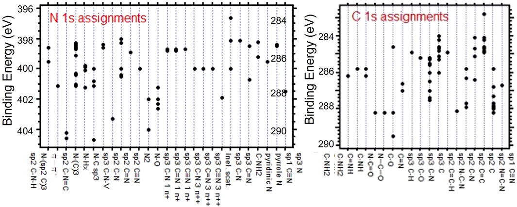
FIGURE 1. Assignments of N 1s and C 1s XPS peak energies published by many groups.
Kusunoki et al. showed XPS analysis of graphite and B-doped semiconducting diamond polycrystalline films grown by microwave plasma chemical vapor deposition (MPCVD) on silicon, bombarded with 300–700 eV N2+ ions (Kusunoki et al., 2000; Kusunoki et al., 2001). Following surface cleaning via annealing (600°C in UHV), the samples were bombarded with N2+ ion beams of 300, 500, and 700 eV at 45° from surface normal. Their assignment of C 1s peaks is opposite to identification in recent studies (Veyan et al., 2018). In addition, no accurate C 1s/N 1s peak associations were reported in Kusunoki et al. (2000) and Kusunoki et al. (2001).
Hellgren et al. (2016) showed similar results to Kusunoki et al., (2000) and Kusunoki et al. (2001). However, their interpretation of the N 1s signal structure is unclear and involves a fifth unexplained peak to achieve the peak deconvolution and curve fitting of the XPS N 1s signal. The proposed N 1s peak assignments, justified by the growth process of their g-CNx thin films, cannot be applied to the N-implanted electronic grade single-crystal diamond (EGSCD) XPS N 1s signal.
The N 1s XPS binding energy (B.E.) region (395–408 eV), observed by different groups (Tabbal et al., 1996; Zheng et al., 1997), revealed the presence of four N 1s peaks at different energies: N1 (398–399 eV); N2 (399–400.5 eV); N3 (401–403 eV); and N4 (∼404 ± 1 eV). The N1 and N2 peaks exhibit the highest intensities. The N3 peak, when visible, has a much lower intensity than N1 and N2. The peak N4 exhibits an even lower intensity than N3. For that reason, prior authors focused more on the assignment of the N1 and N2 peaks and associated the N3 peak with N atoms chemically bonded to O, H, and/or NH impurities. The N4 peak, when reported, was not explained.
A key issue rarely addressed in publications on XPS analysis of materials is the electrical charging of insulators during photoelectron emission, which can be controlled by in situ/real-time low-energy electron bombardment of the sample surfaces to induce neutralization. However, electron beam-induced neutralization must be carefully controlled because it can induce shifts in XPS photoelectron emission energy.
Finally, a new transformational scientific development is that the implantation of low-energy (5,000 eV) N2+ ions at nanoscale depth under the surface of EGSCD modifies the naturally insulating EGSCD surface into an electrically conducting diamond, opening a potential pathway for exploring the development of low-energy N implantation-induced doping for diamond-based electronics.
XPS analyses were performed in a VersaProbe II X-ray photoelectron spectrometer (VPII) (Physical Electronics) featuring an Al Ka monochromatic X-ray source and a vacuum of 4 × 10⁻⁸ Pa (2.8 × 10⁻¹⁰ Torr). All XPS spectra were recorded with a pass-energy of 11.75 eV and an energy step increment of 0.1 eV/step. An electron beam (50 W/15 kV potential) focused on an Al anode surface generated the 200 µm diameter X-ray beam irradiating the sample surface. The angle between the detector and the X-ray beam irradiating the sample surface was 59°.
The VPII has two ion guns: 1) A standard ion gun (SIG), producing ion beams with 100–5,000 eV energies. The SIG produces an N2+ ion beam to implant N atoms into the sample surface/subsurface layers, 2) An argon cluster ion gun (ArCIG), producing an ionized beam formed by clusters of Ar atoms (1,000–2,500 Ar atoms/cluster) that are used to clean surfaces without damage (Veyan et al., 2018).
An electron gun (EG) (neutralizer) generating a low-energy electron beam was used to irradiate the insulator sample surface to compensate for positive charging during X-ray-induced photoelectron emission.
The substrate holder can be tilted along its X-axis to perform angle-resoled XPS (ARXPS) analysis, enabling XPS analysis vs. depth from the sample surface through a depth equivalent to 3 × λ [inelastic mean free path (IMFP) of photoelectrons in materials at a specific kinetic energy (Veyan et al., 2018)]. The other key component of the VersaProbe II XPS system is a substrate holder with heating capability to enable in situ annealing of samples exposed to ion implantation without exposing them to surface contamination in an atmospheric environment.
EGSCD samples [(100) crystalline orientation] with N-atom concentration ≤5 ppb (from Diamond Elements), located on a portable substrate holder, were cleaned by 10 cycles of ArCIB bombardment/30 min each, using an ArCIB beam (2,500 Ar atoms)—20 keV, resulting in 8 eV per Ar atom upon cluster breaking when impacting the sample surfaces under analyses. XPS scans of the cleaned EGSCD surface, shown in Figure 2, revealed no contaminants (O, adventitious C, or N from the atmosphere) or Ar atoms from the ArCIB cleaning.
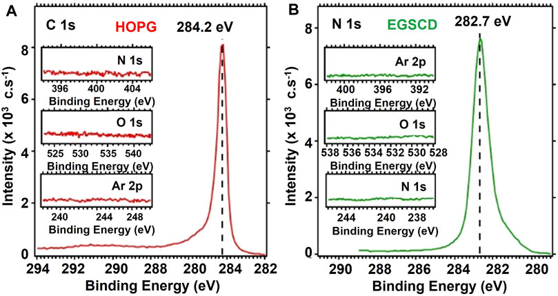
FIGURE 2. XPS spectra from HOPG (A) and EGSCD (B) samples with surfaces cleaned by ArCIB bombardment prior to any N-atom implantation.
A commercial HOPG sample (SPI Supply-grade 1), held by a conductive copper sticky tape on a portable holder, with Scotch tape covering the highly oriented pyrolytic graphite (HOPG) surface, was inserted into the load-lock, and flooded by N2 gas to inhibit water adsorption. The tape was removed, peeling off layers of the HOPG surface, followed by immediate pumping of the load-lock to 4×10⁻⁴ Pa (2.8 x 10⁻¹⁰ Torr), producing a clean HOPG surface.
Most prior research on N-atom implantation in diamond materials to produce nitrogen-C atom vacancy (NV) centers was conducted using external ion accelerators to implant ions with 10–100 s KeV to MeV energy, directed normally to the surface, resulting in deep N atom insertion under the diamond surface, inhibiting production of subsurface NV centers for new generations of quantum-based devices. Two articles described low-energy N ion implantation on diamond (Kusunoki et al., 2000; Kusunoki et al., 2001). However, the low-energy (300–700 eV) N2+ ion bombardment was used to implant N atoms on B-doped semiconducting diamond polycrystalline films grown on silicon substrates. Thus, the R&D described hereafter focused on investigating the implantation of N atoms in EGSCD and HOPG subsurface regions, followed by in situ XPS analysis of atomic chemical bonds, to make critical comparison with prior research on N-atom implantation in C-based materials, including polycrystalline diamond films (Hoffman et al., 1994; Marton et al., 1994; Tabbal et al., 1996; Zheng et al., 1997; Kusunoki et al., 2000; Kusunoki et al., 2001). N atoms were implanted in EGSCD and HOPG surfaces via in situ bombardment with a 5,000 eV N2+ ion beam at 45° incidence from the sample surface, swept uniformly over a 3 × 3 mm2 area. Molecular N2+ ions crack on surface impact, yielding N atoms of half kinetic energy (2,500 eV) that insert into the materials. Details of the cracking of N2+ ions and neutralization into N atoms on impact on solid surfaces have been published in a recent review (Jacobs, 2002). During N-atom implantation in the originally insulating EGSCD surface, the XPS-integrated electron beam neutralizer was used to flood the sample surface to avoid electrical charging by N+ ions.
The N atoms impact the C atoms in the diamond lattice and remove them, creating vacancies (missing C atoms) and inducing the ejection of some C atoms from the surface via the sputtering process. The N2+ ion bombardment induces a two-phase process. Phase 1 consists mainly of N-atom implantation, while Phase 2 involves simultaneous N-atom implantation from cracked N2+ ions impacting the surface and N2+ ion bombardment-induced sputtering of atoms from the material surface.
High-resolution transmission electron microscopy (HRTEM) was performed using a JEOL ARM200F system operated at 200 keV to obtain HRTEM images, selected area electron diffraction (SAED) patterns, and energy-dispersive spectrometry (EDS) analysis, which provides valuable complementary information to XPS analysis, to understand the chemical/nano-structural relationships between the virgin and N-atom-implanted C-based materials. A focused ion beam (FIB) Nanolab Nova200 was used for HRTEM sample preparation, involving a 30 keV to 5 keV Ga+ ion beam. SiO2 or Pt films were grown on sample surfaces to protect them from bombardment by Ga+ ions from the Gaussian beam tail when etching material on both sides of the TEM-lamella sample under preparation.
XPS analyses were performed to confirm the chemical nature of the virgin EGSCD and HOPG surfaces. Figure 2 shows XPS spectra from the C 1s regions of (A) HOPG and (B) EGSCD after cleaning procedures and before any N-atom implantation. The inserts in each panel show the N 1s, oxygen 1s (O 1s), and argon 2p (Ar 2p) B.E. regions.
Figure 2A shows that the peeling process for the HOPG sample in the loading chamber successfully eliminated all surface contamination. Except for the C 1s sp2 peak at 284.2 eV in the C 1s region, no features are visible in the Ar 2p, O 1s, and N 1s regions.
The surface of the EGSCD sample introduced in the XPS chamber had oxygen (O), nitrogen (N), and carbon (C) contamination from the atmosphere. Even a pristine EGSCD sample never used in prior experiments has N atoms because diamond surfaces physically absorb N2 molecules from air. The graphs in Figure 2B show that the ArCIB cleaning process removed all impurity species (O, C, and N) from the sample surface without incorporating any Ar in the subsurface layers. The C 1s sp3 peak located at 282.7 eV relates to a peak shift from the energy characteristic of the C 1s peak in diamond at ∼285.5 eV. The C 1s diamond-related peak shift to lower B.E. is due to the use of the neutralizer during data acquisition, which inserts electrons that affect the energy position of the C 1s peak.
After surface cleaning, HOPG and EGSCD samples were bombarded for 1 min with an N2+ ion beam at 5,000 eV. N2+ ions crack upon impacting the material surface into the N atom and N+ ions. The N+ ions are neutralized by electrons from the neutralizer, inducing N-atom implantation, as explained in detail in Jacobs (2002). The bombardment time of 1 min was long enough to ensure that both EGSCD and HOPG were fully saturated with N atoms, which means that the process had reached phase 2 of the implantation (simultaneous N-atom implantation and N2+ ion bombardment-induced sputtering of atoms from the material surface). The C 1s and N 1s XPS spectra for HOPG and EGSCD after N-atom implantation are shown in Figures 3A, B, respectively. The blue and red dotted lines relate to raw XPS data from EGSCD and HOPG. In the N 1s region, the three N1, N2, and N3 peaks are clearly identifiable, while in the C 1s region, the data depict a feature that can be deconvoluted into two peaks. The vertical dashed lines in Figure 3B point to the energies of each function used to fit the XPS peaks. Iterated Shirley baseline and residue curves are shown in gray.
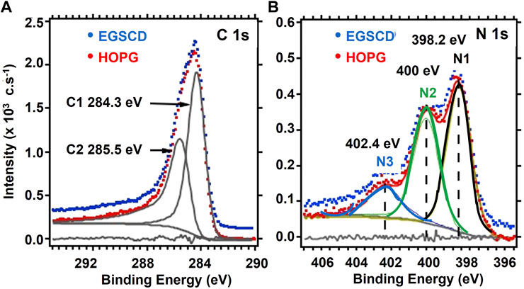
FIGURE 3. XPS spectra for EGSCD and HOPG after 2,500 eV N-atom implantation by N2+ ion bombardment at 5,000 eV: (A) C 1s region; (B) N 1s region. The identification of N1, N2, and N3 peaks in the N 1s region is described in the text.
A key result is that for both HOPG and EGSCD samples, the C 1s and N 1s regions overlap very well, and the N-atom-implanted samples exhibit the same N1 (398.2 eV), N2 (400.0 eV), and N3 (402.4 eV) XPS peaks observed in prior research (Hoffman et al., 1994; Marton et al., 1994; Tabbal et al., 1996; Zheng et al., 1997; Kusunoki et al., 2000; Kusunoki et al., 2001; Hellgren et al., 2016). Apparently, the pristine lattice structure of HOPG or EGSCD does not affect the chemical shifts of the N 1s and C 1s photoelectrons emission after N-atom implantation. The relative concentrations of N ([N]) and C ([C]) atoms in HOPG and EGSCD were calculated using MultiPak software (Physical Electronics), showing [N] = 14% ± 1% and [C] = 86% ± 1%, with respective Relative Sensitivity Factor (RSF) values of 0.499 and 0.314. The calculated concentrations are based on assuming that measured photoelectrons are from C and N atoms uniformly distributed in depth.
The C 1s signal is asymmetric for both HOPG and EGSCD. A deconvolution with two asymmetric peaks at 284.3 eV (C1) and 285.5 eV (C2), shown in Figure 3A, worked best. The tail at higher energies in the C 1s signals, shown in Figure 4A, cannot be explained by C-O, C-Hx, or C-NHx chemical bonds. The deconvolution of the C 1s signal using two asymmetric Voight functions is justified by the conductive nature of the HOPG and EGSCD surfaces, the latter turned from an insulator to electrically conductive by N atoms inserted in the EGSCD lattice. The XPS C 1s signal was previously observed in EGSCD after bombardment with Ar+ ions at 5,000 eV, although EGSCD remained an insulator after Ar-ion implantation (Veyan et al., 2018). The electrical conductivity observed after N-atom implantation in EGSCD is not due to ion-bombardment-induced change of diamond sp3 into graphite sp2 C atom bonds in the N-implanted layer of EGSCD. This effect is discussed at the end of the article as a potential path to new materials science and application to potential new diamond-based micro/nano-electronics.
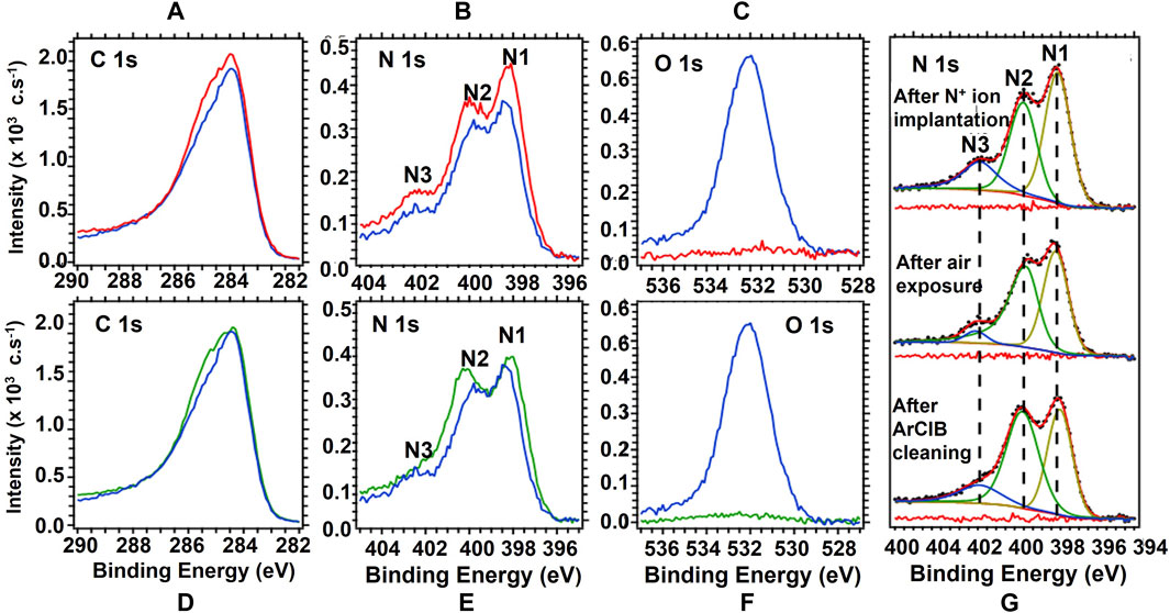
FIGURE 4. Top graphs: XPS spectra from an EGSCD sample after N-atom implantation: (A) C 1s region, (B) N 1s region, and (C) O 1s region. The red curves show data right after N-atom implantation, while the blue curves show data after exposing the N-implanted sample to air. Bottom graphs: XPS spectra from the EGSCD sample after exposure of the N-implanted sample to air: (D) C 1s region, (E) N 1s region, and (F) O 1s region. The blue curves show data after the exposure of the N-implanted sample to air, while the green curves show data after ArCIB bombardment. (G) Peak fitting of the N 1s region after N implantation (top), after subsequent air exposure (middle), and after ArCIB cleaning (bottom). The peak fitting and deconvolution methods are explained in the text. The neutralizer was turned off because the N-implanted EGSCD was electrically conductive.
Following the N-atom implantation in EGSCD, the sample was exposed to a room temperature atmosphere for 48 h and reinserted into the XPS system for XPS analysis, scanning the C 1s, N 1s, and O 1s B.E. regions. Samples were subsequently subjected to 1-min ArCIB surface cleaning, and then XPS analysis of the same B.E. regions was performed. Exposure of the N-implanted EGSCD to air did not affect the nature of the C-N bonds. The O peak visible after air exposure arises from hydrocarbons and water physisorbed on the surface. The intensity and full width at half maximum (FWHM) of the N3 peak are not affected by O, as shown in Figure 4B. Therefore, the N3 peak does not involve O contamination. The three N 1s peaks in Figures 4B, E relate to C-N or N-N bonded atoms and indicate that the HOPG and EGSCD samples are free of O, as shown in Figures 2A, B, and H. The analysis described previously indicates that N2+ bombardment of HOPG and EGSCD does not induce the formation of N-O, C-O, N-Hx, or C-Hx and shows no O 1s peak related to the red curve in Figure 4C, which shows that there is NO contamination from the ion gun generating N2+ ions.
The N 1s signals were fitted by many groups using only Gaussian and/or Voight functions. For the data shown in Figure 3B and Figure 4G, the N1 peak (398.2 eV) and N3 peak (402.4 eV) were fitted with a standard Voight function, while the N2 peak was fitted with an asymmetric Voight function; the latter was chosen based on the ARXPS analysis shown in Figure 5.
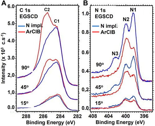
FIGURE 5. ARXPS spectra after N-atom implantation, followed by bombarding the EGSCD for 1 min with a 20 keV ArCIB (8 eV per Ar atom): (A, B) show the C 1s and N 1s regions from the XPS analysis of EGSCD. The blue curves show data for the XPS spectra after N-atom implantation in EGSCD, while the red curves show the data after ArCIB bombardment of the N-implanted EGSCD surface. The top curves, middle curves, and bottom curves show the data at photoelectron take-off angles of 90°, 45°, and 15°, respectively, as indicated in each panel.
After N-atom implantation and before ArCIB bombardment, the relative concentrations of N atoms, represented by the N1, N2, and N3 peaks’ areas, vary slightly with the sampling depth (See Table 1). However, the measurement’s uncertainty is in the order of magnitude of the variation. The main difficulty is to estimate the correct spectrum baseline. The signals are noisy, even over a long acquisition time, to ensure good statistics. The longer acquisition time did not improve the signal quality, which indicates that the depth distribution of N atoms, represented by the N1, N2, and N3 peaks, is uniform. The C/N ratio shown in the right column of Supplementary Table S1 is significantly higher for the take-off angle of 15° than for 45° and 90°, which indicates that more C atoms are present at the surface, as confirmed by the XPS spectra in Figure 5.
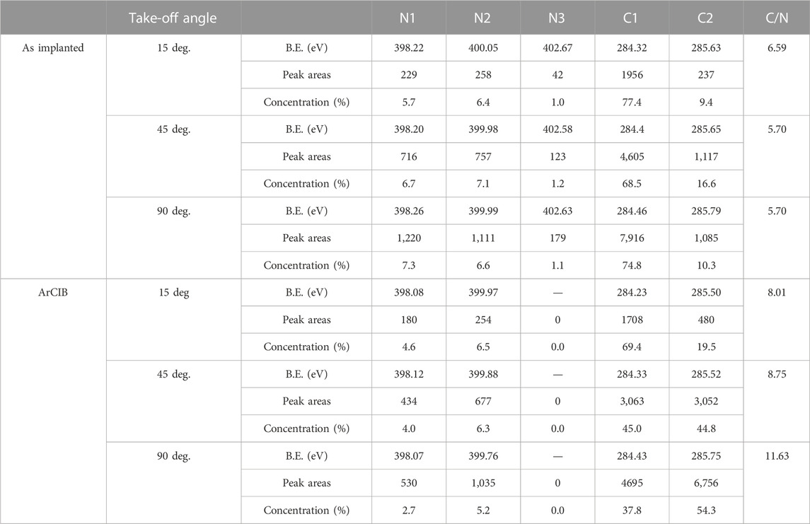
TABLE 1. Peak binding energies in eV at different take-off angles after N2+ bombardment at 5,000 eV and after ArCIG sputtering for 30 s at 20 keV with 2,500 Ar atom size clusters, sample rotated during sputtering at a speed of four rotations per minute, with RSF values of 0.499 for N and 0.314 for C.
Bombardment of the N-implanted EGSCD sample with a 20 keV ArCIB (2,500 Ar atoms) for 1 min induced substantial changes in concentrations of the three N 1s peaks and the C 1s feature. In the N 1s signal, the N3 peak vanished, and the N1 peak decreased in intensity, becoming lower than the N2 peak, as shown in Figure 5B. Alternatively, an increase in intensity of the C 1s - C2 peak, appearing at 285.6 eV, was observed. The C/N ratios for the three take-off angles increased. Nevertheless, the surface is no longer C rich. Indeed, the C/N ratio is now higher at the 90° take-off angle and lower at the 15° take-off angle, as shown in Figure 5A, indicating that the C concentration is now higher in the bulk than at the surface.
In XPS, the total intensity of photoelectrons produced by an element X is given by Eq. 1. The key parameter in Eq. 1 needed to understand the peak area values shown in Table 1 is the density A of the material through which the photoelectrons must travel before exiting the material. For a material made of two elements X and Y, the sum IT of the intensities Ix and Iy is given by:
Considering that the relative concentrations of AX and AY do not vary dramatically, IT should be considered as a constant as a first approximation. A numerical application of Eq. 1 with the values of the peak areas reported in Supplementary Table S1 shows that the total intensity for the take-off angle of 15° for the N-implanted EGSCD varies by 2.6%: IT (15o, N, ArCIB)/IT (15o, N) = 97.4%. Similar numerical calculations for the take-off angle of 45° show a variation of 1.3%:IT (45o, N, ArCIB)/IT (45o, N) = 101.3%. These variations can be explained by cumulative errors during data acquisition and peak fitting procedures. At the 90° take-off angle, the result of Eq. 1 shows a variation of 17.5%: IT (90o, N, ArCIB)/IT (90o, N) = 117.5%. Such a difference can be explained by a system composed of two materials of different densities; the less dense material M1 is on top of the denser material M2. Therefore, if the photoelectrons coming from M2 have an IMFP longer than the thickness of M1, they become detectable for high enough take-off angles. At the 15° and 45° take-off angles, the increase in C content can be correlated to a decrease in N content. If the N atoms contributing to the N1 and N3 peaks were acting as a screening layer, then all the C 1s peaks, as well as the N 1s N2 peak, should increase in intensity, which is not what is observed. After ArCIB-induced sputtering, the area of the C 1s C1 peak decreases by 13% at 15°, 34% at 45°, and 41% at 90°. Simultaneously, the area of the C 1s C2 peak increases by 102.5% at 15°, 173.2% at 45°, and 532% at 90°, as shown in Figure 5A. The ArCIB-induced sputtering might have removed some C atoms, along with N atoms, but that effect would not explain the substantial increase of the C 1s C2 peak shown in Figure 5A. A possible explanation is that, in the C 1s peak, C2 is the sum of two contributions, one from the N-implanted layer and one from the diamond lattice below the N-implanted layer at the surface. This is consistent with the C 1s sp3 B.E. approximately 286 eV and the C 1s sp2 B.E. at 284.2 eV.
In the N 1s signal, the N2 peak exhibited similar intensity (and area) for the three take-off angles shown in Figure 5B, even after ArCIB-induced sputtering, suggesting that the N atoms originating in the N2 peak are strongly bonded to C atoms with the sp3 bonds characteristic of diamond. Alternatively, N atoms contributing to the N3 peak appear as physisorbed. In XPS, the sampling depth is estimated at three times the IMFP of ejecting electrons, which is 5.64 nm (IMFP = 1.88 nm) for diamond. The IMFP may be larger in the N-implanted layer. The N2+ bombardment creates vacancies (missing C atoms in the diamond lattice) and surface roughness. Before ArCIB-induced sputtering, the three N 1s peaks (N1, N2, and N3) had the same relative concentrations for the three take-off angles (see Supplementary Table S1). After ArCIB-induced sputtering, the N3 peak vanished. This effect indicates that when an ArCIB (2,500 Ar atoms) 20 keV beam impacts the sample surface, breaking and releasing 2,500 Ar atoms with ∼8 eV each, these atoms have enough energy to remove N atoms in the surface/subsurface implanted layer that provided the XPS signal from the N atoms contributing to the N3 peak. The evolution of the N 1s N2 peak after ArCIB bombardment follows the same trend as the C 1s C1 peak. The area of the N2 peak decreased by 21.4%, 39%, and 56% at the 15°, 45°, and 90° take-off angles, respectively, suggesting that the N atoms contributing to the N1 peak are chemically bonded to C atoms in the sp2 configuration characteristic of the C bonds in the C1 peak.
Figure 6 shows the HRTEM image and EDS analysis from a cross-section EGSCD prepared by FIB after N-atom implantation. Figure 6A shows a pristine EGSCD area (named SCD) interfacing with a damaged C (a-C) layer (∼8 nm thick) with implanted N atoms. A third area is a SiO2 layer grown on top of the a-C area to protect it from bombardment by the Ga+ ions during FIB fabrication of the cross-section sample for HRTEM. Figures 6B, C show the fast Fourier transform (FFT) for the SCD and a-C layers, respectively. The FFT provides a computationally fast way in HRTEM to implement an algorithm to convert a signal from the space domain into a representation in the frequency domain and vice-versa. This method is used to calculate the structure of atoms, molecules, and solids. It has been used extensively in computational solid-state physics since the 1970s. FFT provides the frequency distribution of the pixel intensities in the HRTEM image, so any periodicity observed in the HRTEM image will provide spots in the FFT. The FFT is interpreted as a “diffraction pattern” providing information on the crystalline structure of a material. In this sense, the FFT from the EGSCD (SCD) (Figure 6B) shows the typical spot pattern confirming the diamond (111) and (110) lattices. On the other hand, Figure 6C shows the FFT pattern for the N-implanted SCD subsurface area. This region, approximately 8 nm deep, appears as a relatively damaged a-C region, revealing spots characteristic of the crystalline diamond lattice and wide rings characteristic of the damaged lattice.
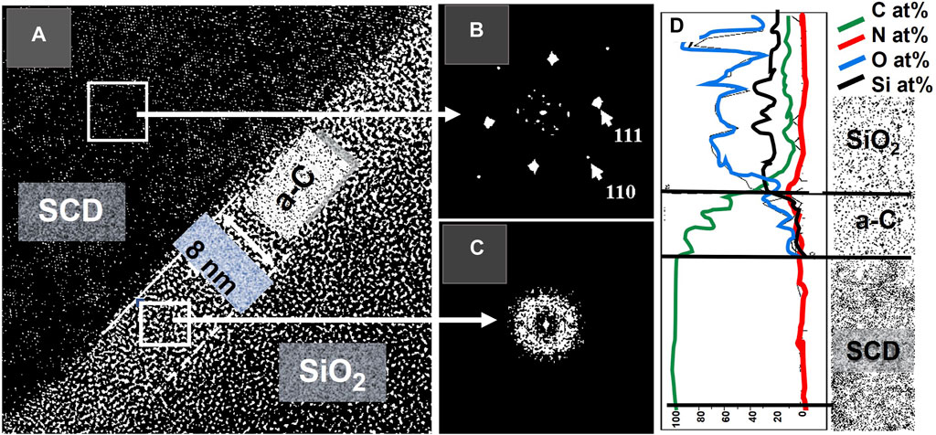
FIGURE 6. (A) HRTEM image of N-implanted EGSCD; the SCD area is pristine diamond; the a-C area (∼8 nm thick) is the EGSCD region that seems to be altered because of the implantation with N atoms. The SCD/a-C interface is well defined and linear at the nanoscale; (B,C) FFT from the SCD and a-C regions, respectively; (D) EDS spectra showing the scan profile of C, N, O, and Si atoms along a line perpendicular to the Si/SCD/a-C interfaces.
Figure 6D shows the distribution of elements through the layered structure of materials present in the prepared HRTEM sample. Electrons from the HRTEM beam excite electrons in the orbitals of atoms, resulting in the emission of characteristic X-rays from the elements present in the material under analysis. The X-ray EDS technique can be performed in STEM mode. The advantage of the EDS in STEM mode compared to the EDS performed in SEM for bulk analysis is that the EDS-STEM mode provides the much higher resolution required for the nanoscale thickness of the sample sections. The EDS spectra related to the scan profile were acquired perpendicularly to the SCD/a-C surface and across the SiO2 layer deposited during FIB preparation of the cross-section sample. The profile shows only C, as expected, in the SCD region. The a-C region reveals a small intensity for Si and O signals, along with the decreasing C signal and a small N signal (N is very difficult to detect), indicating Si and O diffusion during the growth of the SiO2 layer and implanted N atoms.
The experimental results described in Section 3 demonstrate the importance of using complementary material characterization techniques to provide the best possible understanding of the fundamental processes involved in materials development involving the implantation of low-energy N atoms, specifically in diamond. In this sense, implantation of low-energy (≤2,500 eV) N+ ions in EGSCD may enable C-atom ejection from diamond lattice points within 8–10 nm, which is required to form the subsurface NV centers that are currently being intensively explored to produce a transformational new generation of quantum physical electronic devices (Weippert et al., 2023). In addition, diamond-based nano-electronic devices may require producing diamond structures with electrically conductive surface/subsurface nanoscale regions. In this sense, a material’s related effect, which may turn out to be critical for the development of diamond electronics, was observed in the experiments involving the implantation of low-energy N+ ions in EGSCD. The observed effect was that low-energy N-atom implantation in EGSCD induced a diamond surface/subsurface insulator-electrical conductivity transformation, similar to prior research by Auciello et al., which resulted in the development of N-UNCD films with N-atom inserted in grain boundaries, providing electrons for electrical conductivity (Gruen et al., 2004; Villarreal et al., 2022). The hypothesis considered for the explanation of the electrical conductivity of N-UNCD films confirmed by systematic experiments (Gruen et al., 2004; Villarreal et al., 2022) is that the N atoms inserted in grain boundaries react chemically with C atom open bonds, releasing electrons for conduction through the boundaries. The hypothesis to explain the transition of the SCD from insulator to electrically conductive material, due to N atoms implanted in the surface/subsurface region of SCD, is that N atoms link with C atom open bonds around the vacancies, releasing electrons for electrical conduction and is not due to graphitization of the N-implanted surface/subsurface region.
The information presented previously supports the idea of conducting systematic research to determine the viability of low-energy N ion implantation in EDSCD to eventually develop diamond-based nano-electronics and NV-center-based devices.
Further R&D is in progress to obtain information critical to explaining the discovery that implantation of N atoms in EGSCD induce transformation from insulating to an electrically conductive state in the subsurface region.
A systematic study of chemical, structural, and initial electrical properties of EGSCD and HOPG materials was conducted using complementary XPS and HRTEM analyses. The studies involved analysis of sample surfaces inserted in the XPS system, followed by systematic cleaning by ArCIB beams, followed by in situ bombardment with relatively low-energy (5,000 eV) N2+ ions to investigate the effect of N-atom implantation in C-based materials like EGSCD and HOPG.
Key chemical/physical effects were revealed by peaks in the XPS spectra associated with atoms in the C-based materials.
The C1s signal involves a low B.E, revealed by the C1s peak at 284.3 eV, associated with C atoms with the sp2 bond configuration on the top surface and the a-C regions. The high B.E. C1s peak at ∼285.9 eV is associated with C atoms with sp3 diamond bonds, present in the a-C and deep EGSCD regions. The top surface and a-C regions exhibit a damaged C-type structure.
The N 1s signal relates to photoelectrons ejected from the surface and a-C regions implanted with N+ ions. The XPS spectra reveal three peaks, namely N1 (398.2 eV), N2 (400 eV), and N3 (402.4 eV), all related to C-N or N-N chemical bonds. The N 1s N3 peak is not due to N-O, N-H, or N-CHx bonds, as indicated in prior publications. The N1 and N3 peaks are related to weak C-N or N-N bonds linked to C atoms with sp2 bonds, while the N2 peak appears as a stronger C-N bond linked to C atoms with sp3 bonds, characteristic of diamond.
Three material regions are observed in N-implanted EGSCD. The top surface region (∼2–3 nm thick) shows a C/N ratio higher than that of the a-C region. The intermediate a-C region (∼8 nm thick) is implanted with N atoms. The third region is the deep, pristine EGSCD material.
Incorporating N atoms in an EGSCD lattice via N2+ (5,000 eV) ion bombardment induces crystalline structure changes and insulation to electrical conductivity change in the surface/subsurface region. The electrical conductivity induced by N+ ions implanted in the EGSCD surface/subsurface region is currently under systematic investigation by the authors of this article and will be published in the near future.
Assignments of carbon 1s (C 1s) and nitrogen 1s (N 1s) peaks in XPS spectra from carbon nitride (C-N) materials have been discussed in many publications since the 1990s. XPS analysis was used to study chemical bonds between C and N atoms in C3N4 and N atoms implanted in diamond, graphite, graphene, g-C3N4, and carbon nanotubes. Assignment of C 1s and N 1s peaks and C 1s/N 1s peak associations were not clearly described via simulations involving unclear curve fitting of the XPS N 1s signal. Proposed N 1s peak assignments for g-CNx films, for example, cannot be applied to the XPS N 1s signal from N atoms in crystal diamond. Several groups observed N 1s peaks at different energies and with different intensities: N1, N2, N3, and N4. Some groups attributed the N3 peak to N atoms bonded to O, H, and/or NH atmospheric impurities; the N4 peak was not explained. A key issue rarely addressed in XPS analysis of materials is the electrical charging of insulators during photoelectron emission, controllable by in situ electron bombardment that induces the neutralization and energy shift of XPS peaks. Thus, the impact of this investigation relates to providing accurate XPS analysis of carbon-based materials with implanted N atoms at a ≤ 15 nm depth below the surface.
The original contributions presented in the study are included in the article/Supplementary Material; further inquiries can be directed to the corresponding author.
OA: Conceptualization, Funding acquisition, Investigation, Methodology, Project administration, Resources, Supervision, Validation, Writing–original draft, Writing–review and editing. J-FV: Conceptualization, Data curation, Formal Analysis, Investigation, Methodology, Resources, Validation, Writing–review and editing. MA-J: Data curation, Formal Analysis, Methodology, Resources, Writing–review and editing.
The author(s) declare that financial support was received for the research, authorship, and/or publication of this article. This study was supported by the University of Texas at Dallas: Endowment Grant, provided every year to OA.
OA acknowledges the support of the University of Texas at Dallas through his Distinguished Endowed Chair Professor grant provided every year from the endowment funds. J-FV acknowledges the support of the University of Texas at Dallas through his research scientist position in the MSEN Department. MA-J acknowledges the support of the Nano-Characterization Facility at UTD.
The authors declare that the research was conducted in the absence of any commercial or financial relationships that could be construed as a potential conflict of interest.
All claims expressed in this article are solely those of the authors and do not necessarily represent those of their affiliated organizations, or those of the publisher, the editors, and the reviewers. Any product that may be evaluated in this article, or claim that may be made by its manufacturer, is not guaranteed or endorsed by the publisher.
The Supplementary Material for this article can be found online at: https://www.frontiersin.org/articles/10.3389/frcrb.2023.1279356/full#supplementary-material
Gruen, D. M., Krauss, A. R., Auciello, O., and Carlisle, J. A. (2004). N-type doping of NCD films with nitrogen and electrodes made there from. USA patent #6,793,849 B1 (2004).
Hellgren, N., Haasch, R. T., Schmidt, S., Hultman, L., and Petrov, I. (2016). Interpretation of X-ray photoelectron spectra of carbon-nitride thin films: new insights from in situ XPS. Carbon 108, 242–252. doi:10.1016/j.carbon.2016.07.017
Hoffman, A., Gouzman, I., and Brener, R. (1994). Possibility of carbon nitride formation by low-energy nitrogen implantation into graphite: in situ electron spectroscopy studies. Appl. Phys. Lett. 64, 845–847. doi:10.1063/1.110999
Jacobs, D. C. (2002). Reactive collisions of hyperthermal energy molecular ions with solid surfaces. Annu. Rev. Phys. Chem. 53, 379–407. doi:10.1146/annurev.physchem.53.100301.131622
Kusunoki, I., Sakai, M., Igari, Y., Ishidzuka, S., Takami, T., Takaoka, T., et al. (2000). Nitridation of a diamond film using 300–700 eV N+2 ion beams. Diam. Relat. Mater. 9, 698–702. doi:10.1016/s0925-9635(99)00253-8
Kusunoki, I., Sakai, M., Igari, Y., Ishidzuka, S., Takami, T., Takaoka, T., et al. (2001). XPS study of nitridation of diamond and graphite with a nitrogen ion beam. Surf. Sci. 492 (3), 315–328. doi:10.1016/s0039-6028(01)01430-3
Marton, D., Boyd, K., Al-Bayati, A. H., Todorov, S. S., and Rabalais, J. W. (1994). Carbon nitride deposited using energetic species: a two-phase system. Phys. Rev. Lett. 73, 118–121. doi:10.1103/physrevlett.73.118
Tabbal, M., Mérel, P., Moisa, S., Chaker, M., Ricard, A., and Moisan, M. (1996). X-ray photoelectron spectroscopy of carbon nitride films deposited by graphite laser ablation in a nitrogen post discharge. Appl. Phys. Lett. 69, 1698–1700. doi:10.1063/1.118000
Veyan, J.-F., de Obaldia, E., Alcantar-Peña, J. J., Montes-Gutierrez, J., Arellano Jimenez, M. J., José Yacaman, M., et al. (2018). Argon atoms insertion in diamond: new insights in the identification of carbon C1s peak in X-ray photoelectron spectroscopy analysis. Carbon 134, 29–36. doi:10.1016/j.carbon.2018.03.053
Villarreal, D., Sharma, J., Arellano-Jimenez, M. J., Auciello, O., and de Obaldía, E. (2022). Growth of nitrogen incorporated ultrananocrystalline diamond coating on graphite by hot filament chemical vapor deposition. Materials 15 (17), 6003–6015. doi:10.3390/ma15176003
Weippert, J., Engels, J., Quellmalz, P., Giese, C., Luo, T., Mathes, N., et al. (2023). NV-doped microstructures with preferential orientation by growth on heteroepitaxial diamond. J. Appl. Phys. 133, 234401. doi:10.1063/5.0148067
Keywords: XPS, analysis, diamond, graphite, nitrogen, implantation
Citation: Auciello O, Veyan J-F and Arellano-Jimenez MJ (2023) Comparative X-ray photoelectron spectroscopy analysis of nitrogen atoms implanted in graphite and diamond. Front. Carbon 2:1279356. doi: 10.3389/frcrb.2023.1279356
Received: 17 August 2023; Accepted: 26 October 2023;
Published: 21 November 2023.
Edited by:
Anirudha Sumant, Argonne National Laboratory (DOE), United StatesReviewed by:
Abdelrahman Zkria, Kyushu University, JapanCopyright © 2023 Auciello, Veyan and Arellano-Jimenez. This is an open-access article distributed under the terms of the Creative Commons Attribution License (CC BY). The use, distribution or reproduction in other forums is permitted, provided the original author(s) and the copyright owner(s) are credited and that the original publication in this journal is cited, in accordance with accepted academic practice. No use, distribution or reproduction is permitted which does not comply with these terms.
*Correspondence: Orlando Auciello, b3JsYW5kby5hdWNpZWxsb0B1dGRhbGxhcy5lZHU=
†These authors have contributed equally to this work
Disclaimer: All claims expressed in this article are solely those of the authors and do not necessarily represent those of their affiliated organizations, or those of the publisher, the editors and the reviewers. Any product that may be evaluated in this article or claim that may be made by its manufacturer is not guaranteed or endorsed by the publisher.
Research integrity at Frontiers
Learn more about the work of our research integrity team to safeguard the quality of each article we publish.