 Christopher S. Herrmann1
 Sergey V. Baryshev
- 1Department of Electrical and Computer Engineering, Michigan State University, East Lansing, MI, United States
- 2High Power Microwave Section, Naval Research Laboratory, Washington, DC, United States
- 3Department of Chemical Engineering and Materials Science, Michigan State University, East Lansing, MI, United States
Diamond holds promise to reshape ultrafast and high-power electronics. One such solid-state device is the diode avalanche shaper (DAS), which functions as an ultrafast closing switch where closing is caused by the formation of the streamer traversing the diode much faster than 107 cm/s. One of the most prominent applications of DAS devices is in ultrawideband (UWB) radio/radar. Here, we simulate a diamond-based DAS and compare the results to a silicon-based DAS. All DASs were simulated in mixed mode as ideal devices using the drift-diffusion model. The simulations show that a diamond DAS promises to outperform an Si DAS when sharpening the kV nanosecond input pulse. The breakdown field and streamer velocity (∼10 times larger in diamond than Si) are likely to be the major reasons enabling kV sub-50 ps switching using a diamond DAS.
1 Introduction
Ultrawideband (UBW) radio/radar has become a promising area of radio frequency technology and continues to make inroads in communication, sensing, and vision across consumer, commercial, and military sectors. UWB radar has a much wider frequency spectrum of transmitted pulses than conventional radar and radio signals: bandwidth of UWB is often cited as
Ultrashort pulses can be obtained using semiconductor step recovery diodes (SRDs) or Schottky diodes (Choi et al., 2011), but they can only switch a few volts and thus are low peak power. In the 1980s, Si technology for opening (drift SRD or DSRD) (Grekhov et al., 1985) and closing switches (diode avalanche shaper, DAS) (Grekhov et al., 1981) was introduced. DSRDs and DASs are both p-i-n diodes. When stacked, MW-peak-power, low-jitter pulses have been demonstrated with leading and trailing edges in the sub-ns range (Merensky et al., 2009). Advancing DSRD and DAS technology in terms of increasing the voltage rating and decreasing the switching time would be advantageous and critical to further push the envelope of UWB radar capabilities. For instance, recent amendments to spectrum management and telecommunication policies outline UWB radar operating in the 30 GHz band as essential for future vehicular radar technology, which requires a temporal pulse length approaching 10 ps. Other important disciplines could greatly benefit, including ultrafast electro-optics and laser technologies (Woolston, 2012), discharge/plasma-assisted combustion and chemistry (Starikovskaia, 2014), bio-electro-magnetics (Schoenbach et al., 2001), and accelerator systems (Rukin, 2020). In the high-power application space, sufficiently mature DSRD and DAS devices may also be leveraged as high-tech UWB sources of intentional electromagnetic interference (IEMI) (Giri and Tesche, 2004).
Previous work on Si shapers (Chudobiak, 1996) attempted to look beyond Si technology. Direct bandgap GaN and GaAs were ruled out. No reasonable semiconductor offers an improved breakdown field, high mobility, and minority carrier lifetime except for diamond and SiC to potentially outperform Si. A comparison between Si, SiC, and diamond is drawn in Table 1. It should be noted that depending on diamond quality, electron and hole mobility values were reported in the range between 2,000 and 4,500 cm2/V⋅s (Isberg et al., 2002; Pernegger et al., 2005; Nesladek et al., 2008; Girolami et al., 2015; Geis et al., 2018), highlighting the supremacy of diamond in future microelectronics. The most significant parameter is the ultimate differential voltage dV/dt = Ebr × vs, where Ebr is the breakdown electric field and vs is the saturated drift velocity. A comparison between Refs Grekhov et al. (1985) and Johnson (1958) shows that the ultimate differential voltage is exactly the Johnson’s figure of merit (JFOM). For an Si DSRD, the ultimate differential voltage is 2 V/ps. Ideal SiC and diamond DSRD opening switches can offer 90 and 200 V/ps, respectively. This simultaneously provides higher peak power in the GW range with a smaller count of diodes in the stack, a smaller footprint, and reduced cooling requirements. When paired with corresponding SiC and diamond DAS closing switches, ultimate voltage rates between 900 and 2,000 V/ps can ideally be obtained (where an Si DSRD/DAS pair produces ≲20 V/ps). The team at the Ioffe Institute has been actively exploring the potential of SiC technology (Rodin et al., 2006; Ivanov and Grekhov, 2015; Afanasyev et al., 2017). Presented here is an early attempt to assess the potential of diamond for ultrafast high-power switching and pulse-shaping applications.
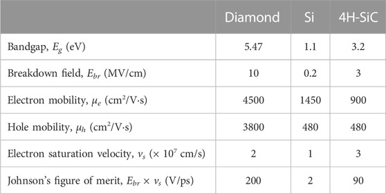
TABLE 1. Comparison of ultimate material properties (IOFFE, 1984; Geis et al., 2018).
2 Pulse shaping and operating principles of diode avalanche shaper
A basic inductive storage pulse shaping circuit arrangement is depicted in Figure 1. The DSRD is an intermediate step between the high-power field effect transistor (FET) that produces the high-voltage nanosecond pulse for the DAS. The role of the DSRD is to properly trigger the DAS. The mating condition between the singular DSRD and the DAS is the JFOM (Rodin et al., 2006): in this context, a DSRD and a DAS made of the same semiconductor would give the best performance, but it is not a primary requirement. The DSRD shapes the pulse coming from the FET from roughly 10 ns to roughly 1 ns and then transfers it to the DAS for final sub-ns shaping. Both the FET and the DSRD are transit time or JFOM limited. In the DAS, ultrafast power shaping to less than 1 ns is achieved through a plasma effect called a streamer that traverses the diode much faster than a charge moving at saturated drift velocity
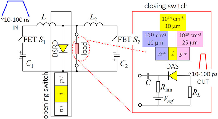
FIGURE 1. High-power ultrafast circuit based on closing and opening switches, adapted from Ivanov and Grekhov (2015) and Focia et al. (1996). The simulated circuit is in the red box.
The pulse sharpening produced by the DAS is due to the streamer formation. The streamer mechanism of electric discharge was originally proposed for gases (Loeb, 1965). Later, streamers were observed and studied in solid-state dielectrics and semiconductors. In p-n junctions, it was proposed that streamer instability is a special type of transient mode of avalanche breakdown (Bartelink and Persky, 1970). The impact ionization front advances as a shock wave. In the wake of this wave, which moves faster than the carrier drift velocity, there is a dense plasma of electrons and holes that fills the depletion region and terminates the electric field. The result is that the diode switches from its initial low conductivity state to a high conductivity state faster than the characteristic carrier transit time.
The key result is that in a DAS, local high charge density traveling at a velocity much higher than the saturated drift velocity exists, thereby overcoming the conventional transit time limitation and allowing much faster switching. To form the streamer, fast overvoltaging (kilovolts on the nanosecond scale, reported as the voltage ramp rate dV/dt) of a reversely biased diode must be provided. With dV/dt ≳1 V/ps, where the state-of-the-art Si DSRD technology can produce 2 V/ps (Grekhov et al., 1985; Focia, 1996), avalanche breakdown does not instantaneously occur despite an applied voltage that can reach a few times higher than the DC breakdown voltage. It should be noted that a stack of Si DSRDs can produce dV/dt much higher than 2 V/ps. The important reference here is a top-of-the-line generator consisting of stacked Si DSRDs that could deliver 80 kV in 1.5 ns, yielding 50 V/ps (Efanov et al., 1997).
First, a displacement current jd associated with a time-varying electric field ∝ ∂E/∂t flows through the diode, forming a pre-pulse voltage across the load (see Figure 2). As an electric field is established across the DAS, charges accelerate and produce electron-hole plasma in the undoped/low-doped, i-layer of the device. This plasma continues to accumulate as
where nd (1014 cm−3 in our case) is the doping concentration in the base layer and Emax of the overvoltaged p-i-n diode is such that Emax/Ebr is approximately 2. Np is the plasma charge concentration that can be estimated as
where Vref is a DC pre-bias. For Li = 10–100 μm, switching takes place on a sub-nanosecond time scale. This is the only non-optical method that allows for conductivity modulation of a semiconductor structure at 100 ps or faster.
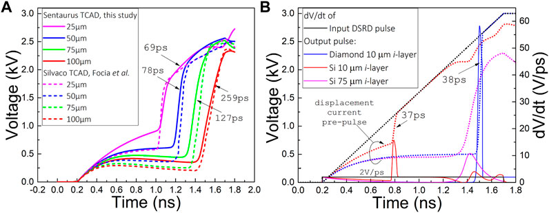
FIGURE 2. Transient analysis of Si and diamond DASs: (A) benchmarking of the Sentaurus TCAD model to the previous results obtained for an Si DAS (Focia, 1996); (B) comparison between a thin-base, 10 μm, Si DAS, a thin-base, 10 μm, diamond DAS, and a thick-base, 75 μm, Si DAS. Arrows denote the full width at half maximum (FWHM) of the output voltage rate dV/dt. Dotted black, blue, red, and magenta lines represent the input pulse from a DSRD, the output pulse from the 10-μm-base diamond DAS, the output pulse from the 10-μm-base Si DAS, and the output pulse from the 75-μm-base Si DAS, respectively. Solid black, blue, red, and magenta lines are time derivatives of the corresponding dotted colored lines.
3 Modelling methodology
Diamond has two main advantages over Si. One is the streamer velocity: from Eq. 1, it can be directly estimated that the streamer velocity of diamond is near or above 108 cm/s, while for Si, it is just above vs (3 × 107 cm/s). Second, for a given thickness, the breakdown voltage of the diamond DAS is larger, and diamond α(E) dependence is shifted to higher fields, resulting in faster multiplication and, thus, a thinner base in the p-i-n structure. Overall, this means that switching enabled by a diamond-based DAS can provide for a much higher output voltage rate than an Si DAS. Evidence for this is seen in Figure 2. The base i-layer is intentionally made ten/twenty-fold thinner than usually anticipated (Grekhov et al., 1981; Focia et al., 1997), and results are compared to an optimized Si DAS design produced by work at the University of New Mexico by Focia (1996). Replicating device doping and geometry studied by Focia et al. allowed for the cross-checking of our computational approach for the Si DAS (Figure 2A). All results presented in Figure 2 were obtained using an input pulse with a 3 kV peak voltage and 1.5 ns linear rise time generated from a hypothetical DSRD.
After validating our computational approach, diamond was implemented as a custom material based on Watanabe’s α(E) data (Watanabe et al., 2001). Watanabe’s data describe diamond with Ebr ∼ 106 V/cm. Because the considered diamond DAS is a heavily punched-through p-i-n diode, its static breakdown voltage Ubr can be estimated as the product of Ebr=106 V/cm and the i-layer thickness of 10 μm, which gives 1 kV. Therefore, the incoming 3 kV pulse provides for three-fold overvoltaging (Emax/Ebr ∼ 3) and guarantees the formation of an ultrafast impact ionization plasma front. Early comparisons seen in Figure 2B favor the 10 μm diamond device over the 75 μm Si device (Focia et al., 1997): the peak output voltage rate (right axis) of the diamond DAS is six times that of the Si DAS, and the diamond DAS exhibits a higher hold-off voltage. Each dotted trace represents a transient voltage curve; the time derivatives of these curves are represented by the solid lines. The black curve shows the input pulse applied to the DAS, while the colored curves represent devices simulated. Comparing the results of Figures 2A,B, it is clear that a thinner base provides for better sharpening but at the cost of smaller output voltage: reducing the i layer thickness of the Si DAS by ten times improved switching from 259 to 37 ps, but output voltage fell from 2 to 0.5 kV. This is while the diamond DAS with a 10 μm i layer switched in 38 ps, providing 2.1 kV of output voltage.
The drift-diffusion approach was used to model the physical behavior of the DAS in three dimensions using the Synopsys Sentaurus TCAD software. This 3D model was configured to simulate constant carrier mobility, carrier velocity saturated at high fields, and avalanche dynamics in accordance with the Van Overstraeten de–Man model (Van Overstraeten and De Man, 1970). Tunneling-assisted impact ionization was not simulated as it is expected to play no role for a DAS based on a wide bandgap material (Rodin et al., 2006). Thermodynamic equations and device self-heating were not modeled, and all simulations took place at 300 K. The DAS devices were simulated in the mixed mode, which allowed for mixed physics and circuit SPICE-like transient analyses. The virtual circuit, shown in Figure 1, consisted of a voltage source connected to the cathode of the diode with the anode connected to a 50 Ω load resistor. The amplitude of the hypothetical DSRD-based voltage source ramped at a constant, linear rate, providing the input voltage with a rise rate of 1–100 V/ps for the DAS to sharpen. A DC voltage source and current limiting resistor were also applied to the cathode of the diode. This allows the breakdown point to be tuned; see Eq. 3. Vref was kept constant at 10 V.
4 Results and discussion
To assess the advanced pulse sharpening capability enabled by diamond, the sharpened output voltage rates dV/dt are compared as a performance figure. There is, of course, no singular metric that can ultimately capture the overall performance of a DAS, as different applications require certain characteristics to be a priority. Nevertheless, the time-derivative of the output voltage curves gives an impression of performance improvement between Si and diamond devices, as seen in Figure 2. A comparison of 10 μm and 75 μm Si devices shows no significant improvement in terms of peak output dV/dt. With all other parameters held equal, the thinner base Si DAS provides for faster switching, consistent with Eq. 2, but hold-off voltage is reduced, and vice versa for the thicker base Si DAS. To further explore dV/dt performance, we compared a 10 μm-base DAS made of Si and one made of diamond. Simulated p-i-n devices with anticipated layer thicknesses and corresponding carrier concentrations are shown in the inset of Figure 1. The Si DAS has light n-doping in the i-layer, like in the classical case (Grekhov et al., 1981). The diamond DAS has light p-doping to reflect intentional or unintentional doping with boron, which has the lowest activation energy among all known dopants. The cross-sectional area of each DAS was 1 mm2.
The performance of the device is dependent on the voltage ramp rate, dV/dt, of the input pulse as shown in Figure 3. The slope of the black line shown in Figure 2B represents this value and is characterized by the ultimate pulse magnitude, dV, and the pulse duration, dt. The value dV/dt can be changed by varying dV and holding dt constant, or vice versa. These methods are not equivalent. The solid lines in Figure 3 show simulations conducted with a constant dt and increasing dV. There is a clear linear relationship between the dV/dt of the input pulse and the peak output voltage rate. The dotted lines in Figure 3 show simulations conducted with shortened dt and constant dV values. Initially, the two methods remain consistent until diverging and leveling off. This divergence is thought to be due to the inability of the crystal lattice, which is to be ionized, to adequately respond to the sub-ns pulses. The crystal lattice does not have enough time to react to the many-kV pulse applied to it (phononic phenomena are on a ∼ns time scale). This divergence occurs despite the device being adequately reverse biased in accordance with the overvoltaging approximation shown in Section 3. The presentation of Figure 3 indicates that future input pulse generators should prioritize ultimate voltage magnitude, but short input pulse duration is still required. A hypothetical diamond DSRD would excel at this.
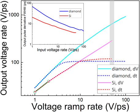
FIGURE 3. Computed peak output voltage rate of a DAS versus input voltage ramp rate from a hypothetical diamond DSRD producing up to 100 V/ps. The performance difference of changing peak amplitude dV or pulse duration dt is emphasized. The difference between a single mated Si and a diamond DSRD/DAS pair is highlighted: the green dumbbell curve should be compared to the full-range solid cyan curve. The inset compares the resultant switching time (FWHM of the output voltage rate dV/dt) as a function of the input voltage ramp rate for an Si DAS and a diamond DAS.
Figure 3 shows that for every given input voltage ramp rate, diamond exhibited a higher output voltage rate. Ultimate input voltage ramp rates ranged from 1 to 100 V/ps, reflecting upon near-future advances in diamond DSRD technology that could enable input pulses with such characteristics; see JFOM in Table 1. Because Si-based DSRD technology can ultimately produce not more than 2 V/ps (Grekhov et al., 1985), multiple Si DSRDs must be stacked together to overcome this 2 V/ps limitation. Performance mismatches of stacked devices may quickly diminish the overall performance. A recent review by Rukin (2020) cites the 80 kV 1.5 ns DSRD generator designed at the Ioffe Institute (Efanov et al., 1997) as the top of the line. From this, 50 V/ps is used as a cut-off input dV/dt that can be produced by the stacked Si technology. In contrast, an ideal singular diamond DSRD could offer 200 V/ps, which would allow for a smaller number of diodes in the stack while promising greater relief on cooling requirements. Therefore, it is instructional to compare the performance of a pair of single Si DSRDs mated with a single Si DAS (semitransparent dumbbell line in Figure 3) with the performance of a mated DSRD-DAS pair made of diamond (full range solid cyan curve in Figure 3). One can see that the simulations predict diamond pulsed power device generation performance improved by orders of magnitude, where the total count of a few diamond diodes can produce an effect that requires several tens or even hundreds of DSRDs or DASs made of silicon.
On a log–log scale, Figure 3 demonstrates that for every given input voltage ramp rate, the output voltage rate increased 30 to 10 times (consistent with the shaping ratio
5 Conclusion and outlook
It was shown computationally that a DAS constructed from diamond exhibits superior performance compared to an identical diode structure made of Si: the output voltage rate was more than three times higher than that of the Si device, which results in a ten-fold increase in the output peak power for the same switching time. Special attention was paid to thin-base devices to test them as ultrafast high peak power pulse shapers and push the envelope in UWB radar applications. This work demonstrates that 5–10 ps MW scale pulses are feasible with single crystal diamond homoepitaxy and efficient n-doping strategies. Diamond homoepitaxy has been continuously improving; however, problems with n-type doping persist with many dopants like nitrogen, phosphorus, and sulfur due to the activation energy of these dopants being much higher than 26 meV (thermal energy at room temperature). Among n-dopants, only phosphorus behaves as a shallow level center, and, therefore, alternative unconventional doping methods like n-type surface doping (Liu et al., 2022) and co-doping (Li et al., 2004) are pursued. Technologically, a canonical vertical p-i-n diamond DAS and DSRD n+ layers can be obtained through fabricating a so-called merged diode (Kubovic et al., 2007), depositing bandgap-matched n-type AlGaN alloy or high-conductivity n-type nanocrystalline diamond (NCD) (Nikhar et al., 2020). The last NCD-based strategy was successfully implemented to fabricate high quality rectifying p-n junctions where n-type NCD was deposited on p-type single crystal diamond (Kohn et al., 2006), SiC (Goto et al., 2014) and even Si (Teii and Ikeda, 2013). Because the n+ NCD layer only serves as a charge collector, it must have low resistance through high carrier concentration and not necessarily through retaining the excellent transport properties of single crystal diamond. When experimenting with merged diodes, other, as-yet-unknown, trade-offs should be established and optimized for.
Data availability statement
The original contributions presented in the study are included in the article/supplementary material; further inquiries can be directed to the corresponding author.
Author contributions
JC and SVB conceived the idea of this study. SVB designed this study. CSH and SVB developed the computational methodology. CSH conducted the computational work. All authors contributed to the article and approved the submitted version.
Acknowledgments
This work was supported by US Department of the Navy under contract No. N6833520C0486. CSH and SVB were partially supported by funding from the College of Engineering, Michigan State University, under Global Impact Initiative.
Conflict of interest
The authors declare that the research was conducted in the absence of any commercial or financial relationships that could be construed as a potential conflict of interest.
The author(s) SVB declared that they were an editorial board member of Frontiers, at the time of submission. This had no impact on the peer review process and the final decision.
Publisher’s note
All claims expressed in this article are solely those of the authors and do not necessarily represent those of their affiliated organizations, or those of the publisher, the editors, and the reviewers. Any product that may be evaluated in this article, or claim that may be made by its manufacturer, is not guaranteed or endorsed by the publisher.
References
Afanasyev, A. V., Ivanov, B. V., Ilyin, V. A., Smirnov, A. A., Kardo-Sysoev, A. F., and Shevchenko, S. A. (2017). A study of 4h-SiC diode avalanche shaper. J. Phys. Conf. Ser. 917, 082002. doi:10.1088/1742-6596/917/8/082002
Bartelink, D., and Persky, G. (1970). Avalanche shock fronts in p-n junctions. Appl. Phys. Lett. 16, 191–194. doi:10.1063/1.1653157
Cavagnaro, M., Pisa, S., and Pittella, E. (2013). Safety aspects of people exposed to ultra wideband radar fields. Int. J. Antennas Propag. 2013, 1–7. doi:10.1155/2013/291064
Choi, G. W., Choi, J. J., and Han, S. H. (2011). Note: picosecond impulse generator driven by cascaded step recovery diode pulse shaping circuit. Rev. Sci. Instrum. 82, 016106. doi:10.1063/1.3523342
Chudobiak, M. J. (1996). New approaches for designing high voltage, high current silicon step recovery diodes for pulse sharpening applications. Ph.D. thesis. Carleton University.
Efanov, V., Kardo-Sysoev, A., Larionov, M., Tchashnikov, I., Yarin, P., and Kriklenko, A. (1997). “Powerful semiconductor 80 kv nanosecond pulser,” in Proc. 11th IEEE International Pulsed Power Conference, Baltimore, MD, USA, 29 June 1997 - 02 July 1997 (IEEE).
Federal Communications Commission (2017). Radar services in the 76-81 ghz band report and order – et docket no 15-26. Washington, D.C: Federal Communications Commission Washington, D.C, 20554.
Focia, R. J., Schamiloglu, E., Fleddermann, C. B., Agee, F. J., and Gaudet, J. (1997). Silicon diodes in avalanche pulse-sharpening applications. IEEE Trans. Plasma Sci. 25, 138–144. doi:10.1109/27.602484
Focia, R. J., Schamiloglu, E., and Fleddermann, C. B. (1996). Simple techniques for the generation of high peak power pulses with nanosecond and subnanosecond rise times. Rev. Sci. Instrum. 67, 2626–2629. doi:10.1063/1.1147191
Focia, R. J. (1996). Ultrafast high power switching diodes. Master thesis. University of New Mexico.
Geis, M. W., Wade, T. C., Wuorio, C. H., Fedynyshyn, T. H., Duncan, B., Plaut, M. E., et al. (2018). Progress toward diamond power field-effect transistors. Phys. status solidi (a) 215, 1800681. doi:10.1002/pssa.201800681
Giri, D., and Tesche, F. (2004). Classification of intentional electromagnetic environments (ieme). IEEE Trans. Electromagn. Compat. 46, 322–328. doi:10.1109/temc.2004.831819
Girolami, M., Bellucci, A., Calvani, P., Cazzaniga, C., Rebai, M., Rigamonti, D., et al. (2015). Mosaic diamond detectors for fast neutrons and large ionizing radiation fields. Phys. status solidi (a) 212, 2424–2430. doi:10.1002/pssa.201532191
Goto, M., Amano, R., Shimoda, N., Kato, Y., and Teii, K. (2014). Rectification properties of n-type nanocrystalline diamond heterojunctions to p-type silicon carbide at high temperatures. Appl. Phys. Lett. 104, 153113. doi:10.1063/1.4871713
Grekhov, I., Efanov, V., Kardo-Sysoev, A., and Shenderey, S. (1985). Power drift step recovery diodes (dsrd). Solid-State Electron. 28, 597–599. doi:10.1016/0038-1101(85)90130-3
Grekhov, I. V., Kardo-Sysoev, A. F., Kostina, L. S., and Shenderey, S. V. (1981). High-power subnanosecond switch. Electron. Lett. 17, 422–423. doi:10.1049/el:19810293
IOFFE (1984). Semicond. Avaliable At: http://www.ioffe.ru/sva/nsm/semicond/.
Isberg, J., Hammersberg, J., Johansson, E., Wikstrom, T., Twitchen, D. J., Whitehead, A. J., et al. (2002). High carrier mobility in single-crystal plasma-deposited diamond. Science 297, 1670–1672. doi:10.1126/science.1074374
Ivanov, P. A., and Grekhov, I. V. (2015). High-voltage sharp-recovery 4h:sic drift diodes: theoretical estimation of limiting parameters. Tech. Phys. 60, 897–902. doi:10.1134/s1063784215060092
Johnson, E. (1958). Physical limitations on frequency and power parameters of transistors. IRE Int. Conv. Rec. 13. 27–34.
Kohn, E., Denisenko, A., Kubovic, M., Zimmermann, T., Williams, O. A., and Gruen, D. M. (2006). A new diamond based heterostructure diode. Semicond. Sci. Technol. 21, L32–L35. doi:10.1088/0268-1242/21/4/l02
Kubovic, M., El-Hajj, H., Butler, J., and Kohn, E. (2007). Diamond merged diode. Diam. Relat. Mater. 16, 1033–1037. doi:10.1016/j.diamond.2006.12.060
Li, R., Hu, X., Shen, H., and He, X. (2004). Co-doping of sulfur and boron in cvd-diamond. Mater. Lett. 58, 1835–1838. doi:10.1016/j.matlet.2003.11.015
Liu, Y., Fu, S., Cheng, S., Gao, N., and Li, H. (2022). Efficient n-type surface doping in diamond. J. Phys. Chem. C 127, 642–648. doi:10.1021/acs.jpcc.2c06884
Loeb, L. B. (1965). Ionizing waves of potential gradient: luminous pulses in electrical breakdown, with velocities a third that of light, have a common basis. Science 148, 1417–1426. doi:10.1126/science.148.3676.1417
Merensky, L. M., Kardo-Sysoev, A. F., Flerov, A. N., Pokryvailo, A., Shmilovitz, D., and Kesar, A. S. (2009). A low-jitter 1.8-kv 100-ps rise-time 50-khz repetition-rate pulsed-power generator. IEEE Trans. Plasma Sci. 37, 1855–1862. doi:10.1109/tps.2009.2025377
Nesladek, M., Bogdan, A., Deferme, W., Tranchant, N., and Bergonzo, P. (2008). Charge transport in high mobility single crystal diamond. Diam. Relat. Mater. 17, 1235–1240. doi:10.1016/j.diamond.2008.03.015
Nguyen, C., and Han, J. (2014). Time-domain ultra-wideband radar, sensor and components: Theory, analysis and design. Springer.
Nikhar, T., Rechenberg, R., Becker, M. F., and Baryshev, S. V. (2020). Dynamic graphitization of ultra-nano-crystalline diamond and its effects on material resistivity. J. Appl. Phys. 128, 235305. doi:10.1063/5.0029132
Pernegger, H., Roe, S., Weilhammer, P., Eremin, V., Frais-Kölbl, H., Griesmayer, E., et al. (2005). Charge-carrier properties in synthetic single-crystal diamond measured with the transient-current technique. J. Appl. Phys. 97, 3417. doi:10.1063/1.1863417
Rodin, P., Ivanov, P., and Grekhov, I. (2006). Performance evaluation of picosecond high-voltage power switches based on propagation of superfast impact ionization fronts in sic structures. J. Appl. Phys. 99, 044503. doi:10.1063/1.2161823
Rukin, S. N. (2020). Pulsed power technology based on semiconductor opening switches: A review. Rev. Sci. Instrum. 91, 011501. doi:10.1063/1.5128297
Schoenbach, K. H., Beebe, S. J., and Buescher, E. S. (2001). Intracellular effect of ultrashort electrical pulses. Bioelectromagnetics 22, 440–448. doi:10.1002/bem.71
Schonland, B. F. J. (1938). Progressive lightning. iv. the discharge mechanism. Proc. R. Soc. Lond. Ser. A, Math. Phys. Sci. 164, 132–150.
Starikovskaia, S. M. (2014). Plasma-assisted ignition and combustion: nanosecond discharges and development of kinetic mechanisms. J. Phys. D Appl. Phys. 47, 353001. doi:10.1088/0022-3727/47/35/353001
Teii, K., and Ikeda, T. (2013). Rectification properties of nanocrystalline diamond/silicon p-n heterojunction diodes. J. Appl. Phys. 114, 093705. doi:10.1063/1.4819385
Van Overstraeten, R., and De Man, H. (1970). Measurement of the ionization rates in diffused silicon p-n junctions. Solid-State Electron. 13, 583–608. doi:10.1016/0038-1101(70)90139-5
Watanabe, T., Irie, M., Teraji, T., Ito, T., Kamakura, Y., and Taniguchi, K. (2001). Impact excitation of carriers in diamond under extremely high electric fields. Jpn. J. Appl. Phys. 40, L715–L717. doi:10.1143/jjap.40.l715
Keywords: ultrawideband, diamond, avalanche breakdown, p-i-n diode, technology computer-aided design
Citation: Herrmann CS, Croman J and Baryshev SV (2023) Computationally assessing diamond as an ultrafast pulse shaper for high-power ultrawideband radar. Front. Carbon 2:1230873. doi: 10.3389/frcrb.2023.1230873
Received: 29 May 2023; Accepted: 31 July 2023;
Published: 24 August 2023.
Edited by:
Hongjun Zeng, Aqua via Rock LLC, United StatesReviewed by:
Etienne Gheeraert, Université Grenoble Alpes, FranceMarco Girolami, National Research Council (CNR), Italy
Copyright © 2023 Herrmann, Croman and Baryshev. This is an open-access article distributed under the terms of the Creative Commons Attribution License (CC BY). The use, distribution or reproduction in other forums is permitted, provided the original author(s) and the copyright owner(s) are credited and that the original publication in this journal is cited, in accordance with accepted academic practice. No use, distribution or reproduction is permitted which does not comply with these terms.
*Correspondence: Sergey V. Baryshev, c2VyYmFyQG1zdS5lZHU=