 Wai Yan Yong
 Andrés Alayón Glazunov
- 1Department of Electrical Engineering, University of Twente, Enschede, Netherlands
- 2Rohde & Schwarz GmbH Co. KG, Munich, Germany
- 3Department of Science and Technology, Linköping University, Linköping, Sweden
This paper presents an antenna-in-package (AiP) design realised with the conventional multi-layer printed circuit board manufacturing method. The design consists of a wideband
1 Introduction
With the advancements in wireless communications and smart device technologies, the Internet of Things (IoTs) has increased with ubiquitous sensing and computing capabilities to connect millions of devices over the internet Mehmood et al. (2017); Aoudia et al., 2024 With the enormous advantages offered by IoT, great attention has been directed towards massive industrial applications such as smart manufacturing Wollschlaeger et al. (2017); Liao et al. (2018), IoT for medical monitoring Kumar and Chand (2020); Da Costa Nascimento et al., 2024, and autonomous driving Minovski et al. (2020). Nonetheless, these IoT applications necessitate using far more sophisticated communication technologies with low latency and ultra-reliable communication networks. Therefore, it is expected that 5G communication will serve as the backbone for the next-generation of wireless devices. 5G wireless communications are anticipated to simultaneously provide peak data rates of up to 10 Gbps to multiple users with low latency ETSI (2013); GSMA Intelligence (2021); Mehmood et al. (2017). The millimetre-wave (mmWave) band has received great interest in achieving this ambitious objective Alibakhshikenari et al., 2021a, Alibakhshikenari et al., 2021b It provides large chunks of wideband spectrum, enabling higher data throughput than in existing networks operating below 6 GHz GSMA Intelligence (2021); Mehmood et al. (2017). However, mmWave signals suffer from increased propagation losses, which can be mitigated by employing array antennas and beamforming technologies Rangan et al. (2014). To that purpose, some array antennas for the mmWave band of 5G have been proposed employing various transmission line technologies such as the traditional waveguide Kim et al. (2014), the gap waveguide Yong et al., 2020, Yong et al. 2022, Yong et al. 2023, and the substrate integrated waveguide Wu et al. (2012); Alibakhshikenari et al., 2021a, Alibakhshikenari et al., 2021b. Although these array antennas offer significantly better loss performance than conventional substrate-based array antennas for the mmWave band, they are typically bulky (due to the operating nature of the waveguide) and more expensive to manufacture. For the successful implementation and widespread deployment of the mmWave 5G band, the hardware implementation must incorporate compact, low-power, and cost-effective features.
To ensure that 5G devices can be produced on a large scale at a low cost and with a small footprint, substrate-based antennas continue to be preferred Burasa et al. (2020); Wagih et al. (2021). However, the microstrip transmission line losses must be minimised for these substrate-based antennas to operate adequately at the mmWave band. To address such requirement, one of the potential approaches is to realise the antenna on-chip Alibakhshikenari et al., 2021a, Alibakhshikenari et al., 2021b However, antennas on-chip usually suffer from high losses. To enhance the performance of the antenna on-chip, the metamaterials can be employed, but this will increase the overall fabrication complexity. Alternatively, antenna-in-package (AiP) technology, which allows active components and antennas to be combined into a single package, has led to dramatically reduced overall interconnect and transmission line losses SalarRahimi et al. (2020); Gu et al. (2019). The loss is reduced because the overall interconnect and transmission line length between the RFIC and antennas can be shortened. Various AiP designs exist in the 5G mmWave bands SalarRahimi et al. (2020); Wagih et al. (2021); Kibaroglu et al. (2018); Yin et al. (2020). However, most of these antennas only cover a portion of the vast 5G mmWave band. This may be attributed to two primary causes. First, most reported works use conventional narrowband patch antennas SalarRahimi et al. (2020); Wagih et al. (2021); Kibaroglu et al. (2018) Although the bandwidth performance of patch antennas can be significantly enhanced by parallel-stacking two of them on two distinct substrate layers and co-optimizing the feeding network and transition design, this results in a significantly higher integration design complexity Yin et al. (2020); Kibaroglu et al. (2018). Second, the majority of analogue beamformers now available on the market cover either the N257 (
This work presents the wideband antenna-in-packaged (AiP) that is realised using the wideband magneto-electric dipole (MED) and integrated with two distinct commercially available analogue beamformers, one covering the N257 band and the other covering the N258 band. The MED antenna is selected in this study as the radiating element of the proposed AiP as it has been widely reported in Luk and Wong (2006); Zhai et al., 2014 as the radiating element for the design of the wideband antenna for base station application. Thus, the proposed AiP is realised using the cost-effective Panasonic Megtron-6 substrate. In this paper, the evaluation of the MED antenna’s performance as an AiP will be discussed in detail. To avoid confusion in the coming discussion in this paper, the MED will be classified into four distinct categories. The design procedure of the MED AiP is summarized as follows:
The main contributions and advantages of the proposed design approach are listed as follows:
The remainder of this article is organised as follows. In Section II, the design principle for the proposed conventional wideband magneto-electric dipole (CMED) antenna, the performance evaluation of the unit cell MED (UMED), and the
2 Design of the wideband MED array antenna
2.1 Conventional MED antenna
The design of our proposed
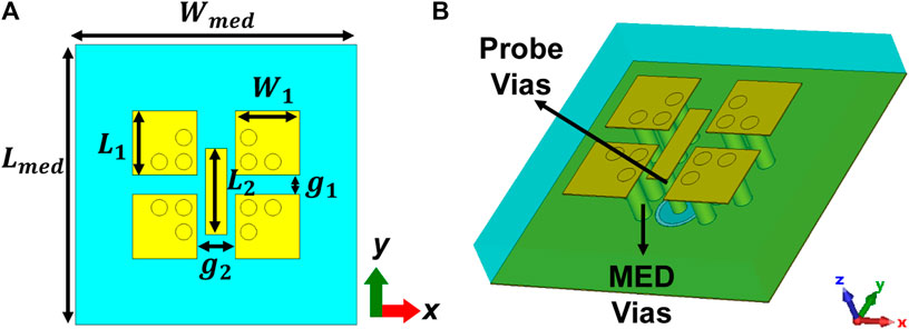
Figure 1. An artist of the proposed MED (A) Top View and (B) Perspective View.
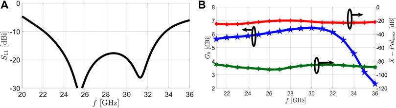
Figure 2. Simulated performance of the proposed CMED antenna fed by L-probe where (A) Simulated
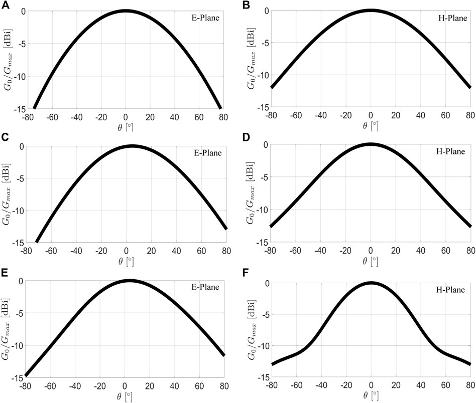
Figure 3. Simulated radiation pattern of the proposed CMED antenna at both E-an H-planes, where plots (A, B) are for 22 GHz, (C, D) are for 28 GHz, and (E, F) are for 32 GHz respectively.
2.2 Unit cell MED and MED array antenna
The CMED design based on the design principle presented in Luk and Wong (2006); Li and Luk (2015) cannot be employed directly for array antenna design due to the large dimensions of the unit cell. The MED unit cell (UMED) dimensions need, therefore, to be adjusted to approximately
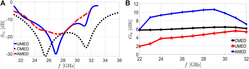
Figure 4. Comparison of the simulated performance for the CMED, UMED and AMED antenna where (A) is the simulated
3
The
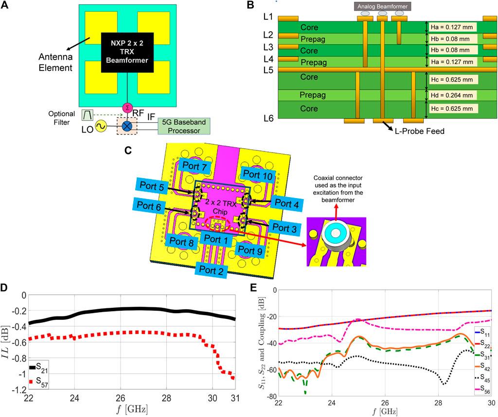
Figure 5. (A)
3.1
As stated above, our challenge is to combine two different beamformers with the proposed MED to form the integrated array antenna. The two analogue beamformers cover a part of the 5G FR2 mmWave band with high linearity performance. The MMW9004KC operating from
3.2 Transition design
In the design of the transition from the analogue beamformer to the AMED antenna, two crucial aspects must be taken into account: (i) a good impedance matching over the intended operating frequency for the transition network between the beamformer and the AMED antenna and (ii) a low mutual coupling between the input/output RF ports of the beamformer at the PCB. Unlike the conventional MED AiP presented in Kuo et al. (2022), which focused only on antenna design, the matching design focuses on the conventional antenna matching technique, where the antenna feeding can be joint tuning with the antenna to obtain the required matching performance and terminated with RF connector. However, this flexibility is absent in an AiP with an active beamformer integrated because the transition design should consider the active beamformer’s packaging. Thus, this section outlines the procedures for designing the transition layer from the beamformer to the antenna. As explained in the previous section, the analogue beamformer only promises good linearity over the frequency band from
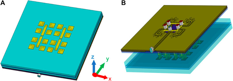
Figure 6. Perspective view of the
3.3 Performance evaluation of the integrated MED
After completing the transition design, it is essential to evaluate the performance of the proposed IMED, including the additional RF transition layer and the additional substrate layers for digital and DC power circuits, which are integrated into a single package. Figure 6 illustrates the proposed
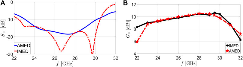
Figure 7. Comparison of the simulated performance of the proposed
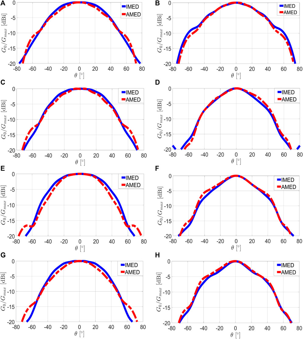
Figure 8. Comparison of the simulated radiation pattern of the AMED and IMED. Results are depicted at different frequencies: 24.25 GHz at the E-plane in (A) and the H-plane in (B), 26 GHz at the E-plane in (C) and the H-plane in (D), 28 GHz at the E-plane in (E) and the H-plane in (F), and 29.5 GHz at the E-plane in (G) and the H-plane in (H).
4 Results and discussion
To validate the proposed solution, two identical IMED antennas were manufactured utilising the standard multilayer PCB fabrication technology. Figure 9 shows one of the fabricated IMED prototypes. It is worthwhile to note that the prototypes for the N257 and N258 bands are identical, except for the integrated analogue beamformers. Although not depicted in Figure 9, it is important to note that an additional DC power supply unit and control board are required to provide the supply and to control the amplitude and phase of the beamformer, respectively.
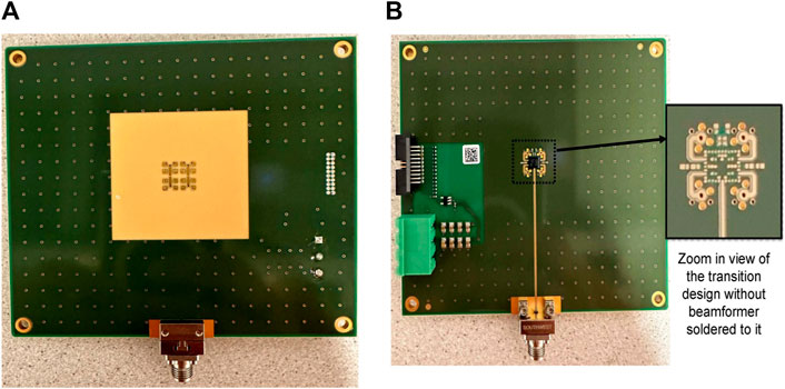
Figure 9. Perspective view of the fabricated
Our prototypes demonstrate the proposed
4.1 Radiation pattern and EIRP measurements
The fabricated IMED prototype is characterised in the far-field using a vector network analyzer and a standard horn antenna using the anechoic chamber in Gapwaves AB, Sweden. It is worthwhile to mention that even though all considerations for reducing systematic errors were addressed during the measurement campaign, a discrepancy of
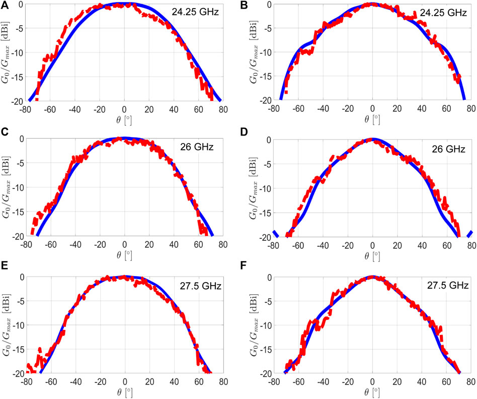
Figure 10. Comparison of the simulated and measured radiation patterns of the AMED and IMED. Results are depicted at different frequencies: 24.25 GHz at the E-plane in (A) and the H-plane in (B), 26 GHz at the E-plane in (C) and the H-plane in (D), and 27.5 GHz at the E-plane in (E) and the H-plane in (F).
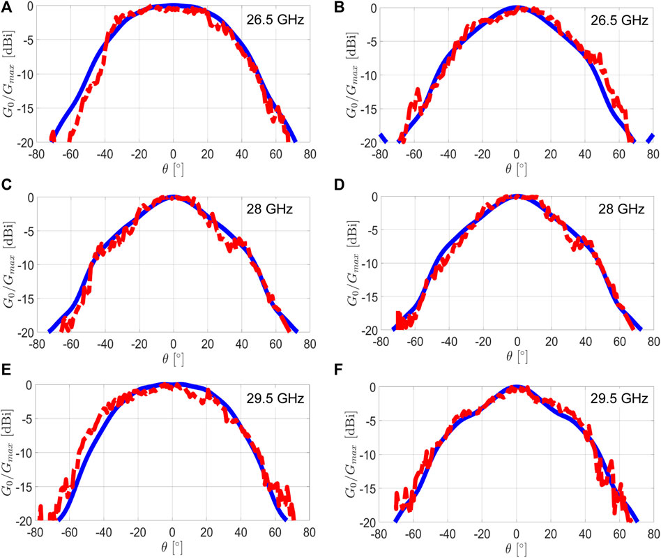
Figure 11. Comparison of the simulated and measured radiation patterns of the AMED and IMED. Results are depicted at different frequencies: 26.5 GHz at the E-plane in (A) and the H-plane in (B), 28 GHz at the E-plane in (C) and the H-plane in (D), and 29.5 GHz at the E-plane in (E) and the H-plane in (F).
Figures 12A,B depict the measured effective isotropic radiated power (EIRP) of manufactured IMED with the two different integrated analogue beamformers. The IMED with MMW 9004 KC achieved the 1 dB compression point
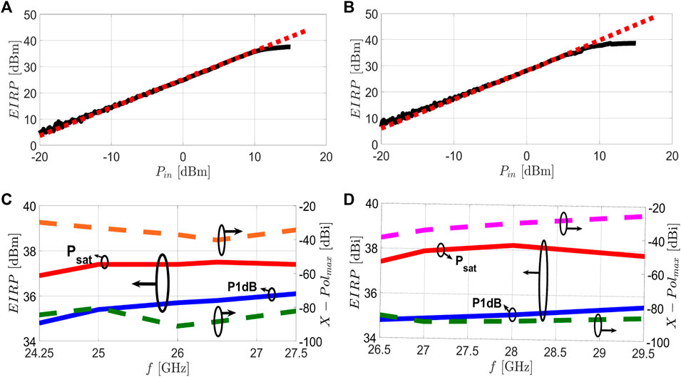
Figure 12. The measured EIRP at the broadside direction
where
4.2 Evaluation of the scanning capability of the proposed IMED as the phased array antenna
Theoretically, suppose the suggested UMED antenna is appropriately designed (with unit cell dimensions around
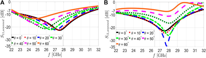
Figure 13. Computed scanning impedance
As well known, the performance of the centre elements can be approximated reasonably well by an infinite array model. However, in realistic array antennas with a finite number of antenna elements, the edge element patterns, and scanned reflection coefficients,
Figure 14 show the computed radiation pattern of the proposed
where the
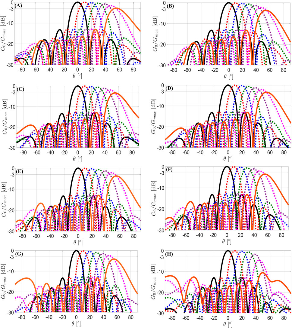
Figure 14. Computed normalised radiation pattern of the proposed IMED with
Another key parameter of the radiation performance of the phased array antenna is the side lobe levels (SLLs). It is worth noting that, in the broadside direction, the SLLs of the proposed MED array antenna are as low as
4.3 Discussion
Table 1 compares the proposed IMED and the currently published AiP or integrated antenna operating at mmWave bands. Our proposed method demonstrates the feasibility of realizing a low-cost AiP with two distinct active beamformers incorporated that operate at different frequencies utilizing a single wideband MED antenna with the same transition design included. Moreover, this can be realized using the cost-effective dielectric substrates commonly employed in the industry while providing adequate radiating performance. Compared to the AiP published in Table 1, all these proposed AiP solutions share one common feature: all are realized based on multilayer stack-up substrates. The table shows that the PCB stack-up complexity is closely related to the polarization (single or dual) the AiP supports. In general, the dual-polarization AiP requires more substrate layers as the antenna feeding design is much more complex compared to a single-polarized antenna.
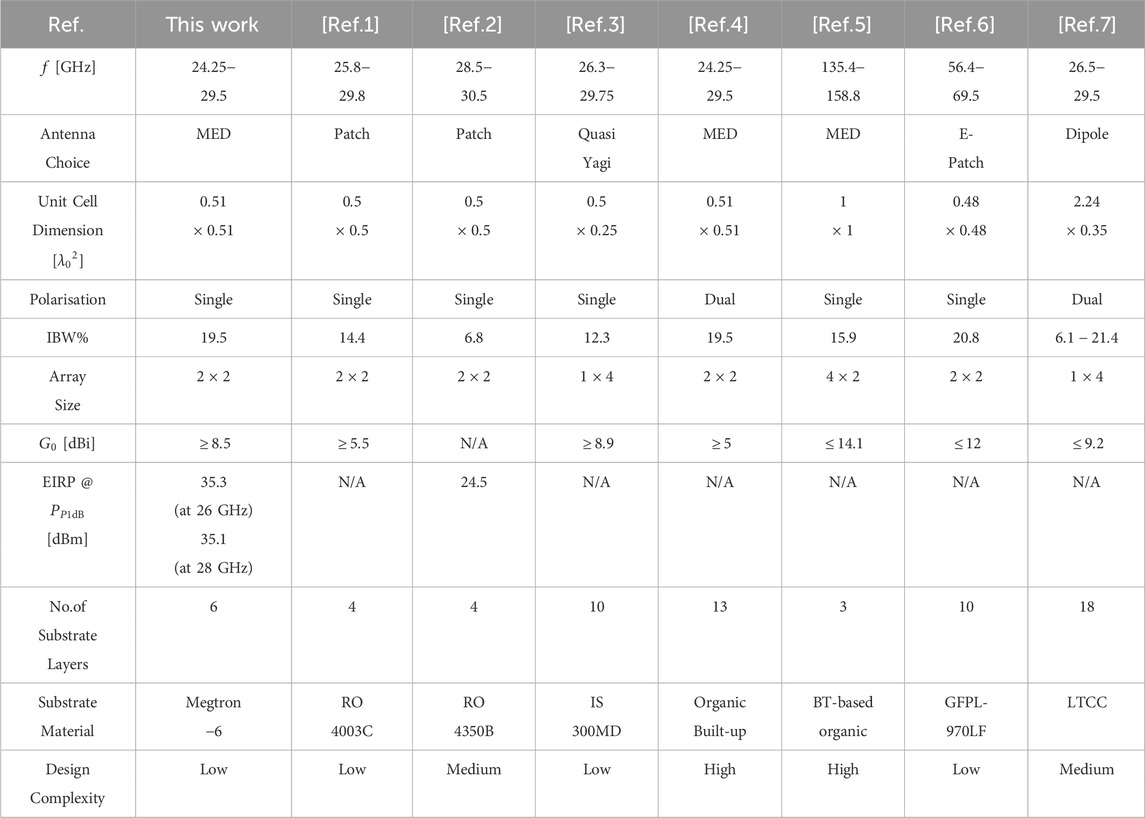
Table 1. Performance comparison of existing AiP for mmWave applications.
Furthermore, to achieve AiP with wideband performance, the patch antenna SalarRahimi et al. (2020); Kibaroglu et al. (2018); Jang et al. (2023), dipole antenna Hwang et al. (2019); Chou et al. (2021), and MED antenna Gu et al. (2021); Kuo et al. (2022) are widely used as radiating elements. Patch antennas are among the most popular radiating elements because they offer a straightforward and inexpensive design. Despite this, patch antennas SalarRahimi et al. (2020); Kibaroglu et al. (2018); Jang et al. (2023) typically support a somewhat limited bandwidth. Additional cutting is necessary to improve these patch antennas’ bandwidth and matching performance. For example, in SalarRahimi et al. (2020), a circular slot is cut across the rectangular patch to improve bandwidth performance, while in Jang et al. (2023), the rectangular patch is modified to an E-shaped patch. The end-fire dipole antenna Hwang et al. (2019); Chou et al. (2021) is another common radiating element used in developing AiP for the same reason as patch antennas. In developing the AiP, the dipole antenna demonstrates a good bandwidth and radiation performance. However, due to the non-planar characteristics, it can only be used to create a linear array AiP. In addition, AiP based on end-fire dipole antennas typically requires more substrate layers, resulting in a significantly more complex fabrication process and higher production costs. Due to its promising bandwidth and radiation performance, a growing interest in using the magneto-electric dipole (MED) Gu et al. (2021); Kuo et al. (2022) antenna has been growing in developing the AiP. As shown in Table 1, MED antennas often offer a substantially wider bandwidth performance while featuring a slightly larger number of substrate layers than microstrip patch antennas. Similar features are observed in our suggested MED design, which supports an impedance bandwidth up to
As mentioned above, the introduction of AiP aims to reduce transmission line loss between the antenna and the RFIC. Nevertheless, it is worth noting that most of the works presented in Table 1 have not considered the impact of the integration with the RFIC. Most of the earlier development of the AiP was targeted toward optimizing the improved radiating performance and manufacturability of the proposed AiP. However, when RFIC integration is considered, the design and fabrication process will have to consider additional aspects of the microwave circuit performance, limiting the design flexibility of the AiP and affecting its overall performance. For instance, without the integration of the RFIC beamformer, the AiP is designed following the conventional antenna design approach using the microstrip line and terminated the antenna port using the RF connector Hwang et al. (2019); Kuo et al. (2022). Nevertheless, the design flexibility is later limited to only the CPW transmission line when the RFIC is integrated. Moreover, the performance of the AiP will also be limited by the performance of the RFIC, which is usually not considered in these AiP designs. Among the earliest works that considered the integration of the RFIC and the antenna performance is the work reported in Kibaroglu et al. (2018). However, due to the limited bandwidth use of the patch antenna and RFIC, the suggested AiP can only deliver an operating bandwidth of 2 GHz, with an EIRP at
To the authors’ best knowledge, no AiP based on MED has been proposed and investigated to integrate with two distinct active beamformers. Therefore, in our presented study, we have investigated the performance of the AiP when the RFIC is integrated with the proposed MED array antenna. The CST simulation evaluated the passive AiP performance, including gain and impedance matching. The manufactured IMED antenna is characterized by the operation of the RFIC and the measurement of EIRP performance. Notably, this study did not give several essential characteristics of the AiP, such as the power consumption of the AiP at different input powers and the power consumption at Tx and Rx modes, since they are intimately related to the operation of the RFIC. However, as the development of the RFIC is not part of the contribution of the presented study and the power consumption at various scenarios of the RFIC is accessible in the NXP data sheet (can be obtained by request to NXP), it is not reported in our paper.
5 Conclusion
This paper presents an antenna-in-package (AiP) design for mmWave 5G applications based on the
Data availability statement
The raw data supporting the conclusions of this article will be made available by the authors, without undue reservation.
Author contributions
AG: Funding acquisition, Methodology, Project administration, Resources, Supervision, Writing–review and editing. WY: Conceptualization, Data curation, Formal Analysis, Investigation, Methodology, Software, Validation, Visualization, Writing–original draft.
Funding
The author(s) declare that financial support was received for the research, authorship, and/or publication of this article. This project received funding from the European Union’s Horizon 2020 research and innovation program under the Marie Sklodowska-Curie grant agreement No. 766231—WAVECOMBE—H2020-MSCA-ITN-2017. Funding from the ELLIIT strategic research environment (https://elliit.se/) is also kindly appreciated.
Acknowledgments
WY and AG were with the University of Twente, Netherlands, when the major part of this research was conducted. The authors would like to thank Gapwaves AB, Sweden, for the financial support for the AiP fabrication and NXP Netherlands for sponsoring the analogue beamformer chip. AG also kindly acknowledges funding from the ELLIIT strategic research environment (https://elliit.se/).
Conflict of interest
Author WY was employed by Rohde & Schwarz GmbH Co.KG.
The remaining author declares that the research was conducted in the absence of any commercial or financial relationships that could be construed as a potential conflict of interest.
The author(s) declared that they were an editorial board member of Frontiers, at the time of submission. This had no impact on the peer review process and the final decision.
Publisher’s note
All claims expressed in this article are solely those of the authors and do not necessarily represent those of their affiliated organizations, or those of the publisher, the editors and the reviewers. Any product that may be evaluated in this article, or claim that may be made by its manufacturer, is not guaranteed or endorsed by the publisher.
References
Alibakhshikenari, M., Virdee, B. S., Salekzamankhani, S, et al. (2021a). High-isolation antenna array using SIW and realized with a graphene layer for sub-terahertz wireless applications. Scientific Reports 11, 10218. doi:10.1038/s41598-021-87712-y
Alibakhshikenari, M, Virdee, B. S., Althuwayb, A. A., et al. (2021b). Study on on-chip antenna design based on metamaterial-inspired and substrate-integrated waveguide properties for millimetre-wave and thz integrated-circuit applications. Journal of Infrared, Millimeter, and Terahertz Waves 42, 17–28. doi:10.1007/s10762-020-00753-8
Alhamed, A., Gültepe, G., and Rebeiz, G. M. (2022). A multi-band 16–52-GHz transmit. IEEE J. Solid-State Circuits 57, 1280–1290. doi:10.1109/jssc.2021.3134325
Aoudia, M., Alaraj, M. B., Abu Waraga, O., Mokhamed, T., Abu Talib, M., Bettayeb, M., et al. (2024). Toward better blockchain-enabled energy trading between electric vehicles and smart grids in Internet of Things environments: a survey. Frontiers in Energy Research 12, 1393084. doi:10.3389/fenrg.2024.1393084
Burasa, P., Djerafi, T., and Wu, K. (2021). A 28 GHz and 60 GHz dual-band on-chip antenna for 5G-compatible IoT-served sensors in standard CMOS process. IEEE Trans. Antennas Propag. 69, 2940–2945. doi:10.1109/tap.2020.3025236
Chou, H. T., Chou, S. J., Deng, J. D., Chang, C. H., and Yan, Z. D. (2022). LTCC-based antenna-in-package array for 5G user equipment with dual-polarized Endfire radiations at millimeter-wave frequencies. IEEE Trans. Antennas Propag. 70, 3076–3081. doi:10.1109/tap.2021.3118819
Da Costa Nascimento, J. J., Marques, A. G., Adelino Rodrigues, Y. O., et al. (2024). Health of Things Melanoma Detection System—detection and segmentation of melanoma in dermoscopic images applied to edge computing using deep learning and fine-tuning models. Frontiers in Communications and Networks 5, 1376191. doi:10.3389/frcmn.2024.1376191
GSMA Intelligence (2021). The Economics of mmWave 5G - an assessment of total cost of ownership in the period to 2025. Tech. Rep. Qualcomm Technol.
Gu, X., Liu, D., Baks, C., Tageman, O., Sadhu, B., Hallin, J., et al. (2019). Development, implementation, and characterization of a 64-element dual-polarized phased-array antenna module for 28-GHz high-speed data communications. IEEE Trans. Microw. Theory Tech. 67, 2975–2984. doi:10.1109/tmtt.2019.2912819
Gu, X., Liu, D., Hasegawa, Y., Masuko, K., Baks, C., Suto, Y., et al. (2021). Antenna-in-package integration for a wideband scalable 5G millimeter-wave phased-array module. IEEE Microw. Wirel. Components Lett. 31, 682–684. doi:10.1109/lmwc.2021.3071917
Hwang, I. J., Ahn, B., Chae, S. C., Yu, J. W., and Lee, W. W. (2019). Quasi-Yagi antenna array with modified folded dipole driver for mmWave 5G cellular devices. IEEE Antennas Wirel. Propag. Lett. 18, 971–975. doi:10.1109/lawp.2019.2906775
Jang, T. H., Jung, K. P., and Park, C. S. (2023). Broadband millimeter-wave antenna in package with L-probed E-shaped patch covering 57 GHz to 71 GHz. IEEE Trans. Antennas Propag. 71, 89–98. doi:10.1109/tap.2022.3215225
Kibaroglu, K., Sayginer, M., and Rebeiz, G. M. (2018). A low-cost scalable 32-element 28-GHz phased array Transceiver for 5G communication Links based on a 2 × 2 beamformer Flip-chip Unit cell. IEEE J. Solid-State Circuits 53, 1260–1274. doi:10.1109/jssc.2018.2791481
Kildal, P. S. (2015). Foundations of antenna engineering: a unified approach for line-of-sight and multipath. London, United Kingdom and Boston, United StatesArtech House.
Kim, D., Hirokawa, J., Ando, M., Takeuchi, J., and Hirata, A. (2014). 64 × 64-Element and 32 × 32-element slot array antennas using Double-layer Hollow-waveguide Corporate-feed in the 120 GHz band. IEEE Trans. Antennas Propag. 62, 1507–1512. doi:10.1109/TAP.2013.2296318
Kumar, M., and Chand, S. (2020). A secure and efficient cloud-centric internet-of-medical-things-enabled smart healthcare system with public verifiability. IEEE Internet Things J. 7, 10650–10659. doi:10.1109/jiot.2020.3006523
Kuo, H. C., Kuo, C. W., Wang, C. C., and Hung, C. P. (2022). A D-band magneto-electric dipole antenna-in-package (AiP) implemented on BT-based organic substrate. IEEE Trans. Components, Packag. Manuf. Technol. 12, 1673–1680. doi:10.1109/tcpmt.2022.3211500
Li, M., and Luk, K. M. (2015). Wideband magneto-electric dipole antenna for 60-GHz millimeter-wave communications. IEEE Trans. Antennas Propag. 63, 3276–3279. doi:10.1109/tap.2015.2425418
Liao, Y., de Freitas Rocha Loures, E., and Deschamps, F. (2018). Industrial Internet of Things: a systematic literature review and insights. IEEE Internet Things J. 5, 4515–4525. doi:10.1109/jiot.2018.2834151
Luk, K. M., and Wong, H. (2006). A new wideband unidirectional antenna element. Int. J. Microw. Opt. Technol. 1, 35–44.
Mak, C. L., Luk, K., Lee, K., and Chow, Y. (2000). Experimental study of a microstrip patch antenna with an L-shaped probe. IEEE Transactions on antennas and propagation 48, 777–783. doi:10.1109/8.855497
Mehmood, Y., Haider, N., Imran, M., Timm-Giel, A., and Guizani, M. (2017). M2M communications in 5G: state-of-the-art architecture, recent advances, and research challenges. IEEE Commun. Mag. 55, 194–201. doi:10.1109/mcom.2017.1600559
Minovski, D., Åhlund, C., and Mitra, K. (2020). Modeling quality of IoT experience in autonomous vehicles. IEEE Internet Things J. 7, 3833–3849. doi:10.1109/jiot.2020.2975418
Rangan, S., Rappaport, T. S., and Erkip, E. (2014). Millimeter-wave cellular wireless networks: Potentials and challenges. Proc. IEEE 102, 366–385. doi:10.1109/jproc.2014.2299397
SalarRahimi, M., Vilela Pinto dos Anjos, E., Taghikhani, P., Volski, V., Fager, C., Schreurs, D. M. M. P., et al. (2020). A cost-efficient 28 GHz integrated antenna array with full impedance matrix characterization for 5G NR. IEEE Antennas Wirel. Propag. Lett. 19, 666–670. doi:10.1109/lawp.2020.2976188
Theis, G., Song, Z., Federico, G., Caratelli, D., and Smolders, A. B. (2021). A design framework for beamforming integrated circuits operating at mm-wave frequencies. IEEE Access 9, 62232–62240. doi:10.1109/access.2021.3073987
Wagih, M., Hilton, G. S., Weddell, A. S., and Beeby, S. (2022). Millimeter-wave power transmission for compact and large-area Wearable IoT devices based on a higher Order mode Wearable antenna. IEEE Internet Things J. 9, 5229–5239. doi:10.1109/jiot.2021.3107594
Wollschlaeger, M., Sauter, T., and Jasperneite, J. (2017). The future of industrial communication: Automation networks in the era of the internet of things and industry 4.0. IEEE Ind. Electron. Mag. 11, 17–27. doi:10.1109/mie.2017.2649104
Wu, K., Cheng, Y. J., Djerafi, T., and Hong, W. (2012). Substrate-integrated millimeter-wave and terahertz antenna technology. Proc. IEEE 100, 2219–2232. doi:10.1109/jproc.2012.2190252
Yin, Y., Zihir, S., Kanar, T., Ma, Q., Chung, H., Gao, L., et al. (2020). A 37-42-GHz 8x8 phased-array with 48-51-dBm EIRP, 64-QAM 30-Gb/s data rates, and EVM Analysis versus channel RMS errors. IEEE Trans. Microw. Theory Tech. 68, 4753–4764. doi:10.1109/tmtt.2020.2998183
Yong, W. Y., Hadaddi, A., and Glazunov, A. A. (2023). Design and characterization of the fully metallic gap waveguide-based frequency selective radome for millimeter wave fixed beam array antenna. IEEE Trans. Antennas Propag. 71, 531–541. doi:10.1109/tap.2022.3215454
Yong, W. Y., Haddadi, A., Emanuelsson, T., and Glazunov, A. A. (2020). A bandwidth-enhanced cavity-backed slot array antenna for mmwave fixed-beam applications. IEEE Antennas Wirel. Propag. Lett. 19, 1924–1928. doi:10.1109/lawp.2020.3022988
Keywords: antenna-in-package (AiP), fifth generation (5G), millimeter-wave (mmwave), ME-dipole, phased array antenna
Citation: Yong WY and Glazunov AA (2024) Wideband
Received: 22 May 2024; Accepted: 08 July 2024;
Published: 20 August 2024.
Edited by:
Bal Virdee, London Metropolitan University, United KingdomReviewed by:
Lida Kouhalvandi, Doğuş University, TürkiyeMohammad Alibakhshikenari, Universidad Carlos III de Madrid, Spain
Copyright © 2024 Yong and Glazunov. This is an open-access article distributed under the terms of the Creative Commons Attribution License (CC BY). The use, distribution or reproduction in other forums is permitted, provided the original author(s) and the copyright owner(s) are credited and that the original publication in this journal is cited, in accordance with accepted academic practice. No use, distribution or reproduction is permitted which does not comply with these terms.
*Correspondence: Andrés Alayón Glazunov, YW5kcmVzLmFsYXlvbi5nbGF6dW5vdkBsaXUuc2U=