
94% of researchers rate our articles as excellent or good
Learn more about the work of our research integrity team to safeguard the quality of each article we publish.
Find out more
ORIGINAL RESEARCH article
Front. Commun. Netw., 11 June 2021
Sec. Non-Conventional Communications and Networks
Volume 2 - 2021 | https://doi.org/10.3389/frcmn.2021.688419
E-textiles have received tremendous attention in recent years due to the capability of integrating sensors into a garment, enabling high-precision sensing of the human body. Besides sensing, a number of solutions for e-textile garments have also integrated wireless interfaces, allowing sensing data to be transmitted, and also inbuilt capacitive touch sensors, allowing users to provide instructions. While this has provided a new level of sensing that can result in unprecedented applications, there has been little attention placed around on-body edge computing for e-textiles. This study focuses on the need for a noninvasive and remote health-monitoring solution with inbuilt on-body edge computing, and how enabling such sensing and computing capabilities in a fabric environment can act as a new method for healthcare monitoring through the use of embedded computing intelligence in smart garments. Facilitating computing in e-textiles can result in a new form of on-body edge computing, where sensor information is processed very close to the body before being transmitted to an external device or wireless access point. This form of computing can provide new security and data privacy capabilities and, at the same time, provide opportunities for new energy-harvesting mechanisms to process the data through the garment. This study proposes this concept through embroidered programmable logic arrays (PLAs) integrated into e-textiles. In the same way that PLAs have programmable logic circuits by interconnecting different AND, NOT, and OR gates, we propose e-textile–based gates that are sewn into a garment and connected through conductive thread stitching. Two designs are proposed, and this includes single- and multi-layered PLAs. Experimental validations have been conducted at the individual gates and the entire PLA circuits to determine the voltage utilization and logic computing reliability. The multilayered PLA garment superseded the single-layered garment with higher levels of accuracy in the yielded results due to the enhanced design layout, which reduces the potential for short circuits and errors occurring. Our proposed approach can usher in a new form of on-body edge computing for e-textile garments for future wearable technologies, and, in particular, with the current pandemic that requires noninvasive remote health-monitoring applications.
Electronic textiles (E-textiles) provide the ability to integrate electronic components and devices into garments (Fernández-Caramés & Fraga-Lamas, 2018; Chiuchisan et al., 2019). Numerous solutions have been developed where sensors are integrated into the garment to perform sensing that is close to the body. Examples of these sensing capabilities include electrocardiography (ECG) (Ramasamy and Balan, 2018), temperature (Lugoda et al., 2018), and pressure (Yang et al., 2019). This technological development of integrating sensory devices into garments has resulted from advancements in nanotechnology materials, microelectronics, and traditional garment fabrication technology such as conductive threads and yarns (Parvinzadeh Gashti et al., 2016; Ismar et al., 2020). Numerous applications have resulted in sensor-based e-textile garments, including new techniques to monitor human physiological conditions and rehabilitation techniques, and sports performance monitoring (Kubicek et al., 2020).
However, one capability that current e-textiles lack is embedded computing functionality to compute these sensor devices. Solutions have been proposed to have computing processors integrated into the garments by embroidering low-computational computing chips (Al-huda Hamdan et al., 2018). These chips usually have inbuilt Boolean logic circuitries that can process such sensor information and, in many cases, also integrate wireless interfaces to enable transmission of the information to an external device (Mecnika et al., 2015; Gonçalves et al., 2018). However, disadvantages of these current techniques of integrating these electronics-based chips into the garment exist. The form of the garment changes due to the embroidering of the electronic chips onto the fabric, and the physical shape of and the protruding sharp edges on the chips can potentially lead to injury or discomfort of the user or other individuals in close proximity through scratching.
This study proposes an alternative and new technique in conducting on-body edge computing (Hassan et al., 2019; Yu et al., 2018). We propose embroidering programmable capabilities directly into the garment to allow the Boolean logic circuits to be reconfigured to facilitate new applications or changes in the user’s requirements, providing a more personalized and safer approach to health monitoring at an individual level. The proposed approach uses the concept of programmable logic arrays (PLAs) found in typical electrically erasable programmable read-only memory (EEPROM) chips and embroiders the logic gate circuit directly into a garment. The programmable capability comes in the form of interchanging the stitching connections between the wired bus planes (horizontal and vertical wires) from the different logic gates, in the very same way that the connections between the wired busses in the EEPROM can be reprogrammed. Our proposed solution also creates a layer of privacy, where the computing is performed on the garment itself and through wired connections, where data from the sensors are computed through the logic circuits, and the output can be a summary (e.g., “Yes” or “No”) of data that are transmitted wirelessly.
To adopt such embedded PLA programmable capabilities within the garment environment, our study presents two varying design prototypes: 1) single-layered design and 2) multilayered design. The study does not go through the full solution of linking the sensor data to the logic circuits to be computed but rather only focuses on the design and implementation of the embroidered logic gate circuitry and validation of the embroidered PLA performance. The performance analysis includes analyzing individual embroidered logic gate circuits and cross-comparing the accuracy and performance of both design circuits. Our analysis found that the design through a multilayered architecture leads to a reliable circuit that minimizes short circuits between the wired bus planes and also enables easy reconfiguration of the connections. The validation phase demonstrates the clear advantage the multilayered design has over the single-layer design based on the voltage validation and performance results yielded. From a voltage performance perspective, the multilayered design OR gate output readings (Z1 and Z2) were, on average, double the voltage levels of the single-layered OR gate output readings (Z1 and Z2), indicating a higher level of performance for the multilayered design.
The study is organized as follows: Section II presents the concept of PLAs for e-textile garments. Section III discusses the development of individual logic gates, while section IV presents two designs of the PLA on the e-textile garment. Section V presents the results from the experimental analysis, and finally, Section VI presents the conclusion.
Our proposed solution is illustrated in Figure 1, where the PLA circuit is embroidered and stitched directly into the garment. We will first describe the concept of the PLA, the configuration of the PLA, and enabling the Boolean expression to align to two health-focused use cases.
PLAs are programmable logic devices that can create dynamic logic computing circuits. To enable the design and development of a reconfigurable “on-body edge computing” garment, the programmable logic array has a fixed architectural logic gate design, along with programmable AND and OR logic gate capabilities through their respective embroidered connecting planes. Since the PLA enables all the gates to be programmed, this can provide the digital circuitry architecture to meet the modular, personalized, and reusable capabilities required for the “on-body edge computing” garment. Taking this PLA architecture approach, we looked at the methodology and steps that need to be completed in order to embed PLA technology within a garment structure using embroidery techniques as an enabler.
To map the embroidered PLA garment to a health application use case, a truth table was defined to show the visual representation of the switching functionality of the PLA. A three-input truth table having eight input combinations and two outputs was adopted, represented by Z1 and Z2 logic levels. The truth table input combinations and output results were based on two health-monitoring scenarios: 1) hypertension and 2) epilepsy. Hypertension is related to high blood pressure levels in a human, and symptoms vary from irregular heartbeats to chest pains and difficulties in breathing (Fuchs and Whelton, 2020). Epilepsy is a common brain disease characterized by recurring seizures. Seizures are usually of two types, either beginning in one part of the brain (localized, focal, or partial seizures) or in both brain hemispheres simultaneously (generalized seizures). In the case of focal seizures, patients may or may not be aware of the start of the seizure. Symptoms can include sensory experiences (unusual taste, smell, or epigastric sensation) and involuntary and repetitive movements of body parts. Seizures may also be associated with prodromal temperature fluctuations (Dubé et al., 2009; Szelényi and Komoly, 2018). The input variables in the smart garment PLA truth table are focused on representing sensor input readings linked to temperature, blood pressure, and heart rate, where these variables align in certain cases to a raised alert notification. A defined threshold level for each sensor input reading was selected and set in order to represent logic level “1” and logic level “0” (Figure 1).
Taking the defined truth table, we deciphered the truth table Boolean expression, using the laws of Boolean algebra to reduce the logic function (Z1 and Z2) to its minimal form. From the above computations (Figure 1), we can see that for the garment PLA configuration, we require six input connectors, three AND logic gates, and 2 OR logic gates in order to design a PLA “on-body edge computing” garment.
The embroidered circuit gates will include electronic components (transistors and resistors) and conductive threads that will create the wired bus and the interconnection between the planes of the gates. A number of challenges will be faced in stitching the PLA into the fabric. First, energy will be dissipated at a very fast rate due to the circuitry to perform the logic computation. At the same time, this also heavily depends on the arrangement of the embroidered circuits and their connections to minimize the path that will result in energy dissipation as the current is traveling between the gates. The next challenge lies in the efficient delivery of power and ground for each of the gates, ensuring that this will not result in short circuits. Such short circuits can result from overlapping that may occur if the wired bus connections come into contact, due to the movements and stretching of the garments.
Following the identification of the required number of core logic gates for the PLA configuration, the next steps involve the process of implementing the design of the logic gates in an embroidered digitized format that in turn can be sewn using an embroidery machine into a garment’s fabric back panel. The back panel of a garment was selected due to it being the largest surface area available for the placement and manipulation of the logic gates. Here, we detail the process utilized for the creation of individual gates, including the input connections (inverter logic gates), AND logic gates, and OR logic gates.
In order to construct the logic gates, the equivalent analog circuit was used as a base design guideline. The logic gates were designed based on RTL (resistor–transistor switches), allowing the logic gate inputs to be connected directly to the base of the transistor switches. Through the combination of these embroidered RTL circuits with varying inputs that make up the embroidered textile-based PLAs, we can produce alert notification outputs linked to the hypertension and epilepsy health-sensing use case truth table design.
The graphic design of a logic gate embroidery circuit takes into consideration the space, position, and placement of the resistors, transistors, and power and ground connections, and also the overall acceptable size of such a logic gate for it to be practically usable within a garment structure. The development of the embroidered digitized version of the circuit utilizes a “satin stitch” type of embroidery.
The above process was repeated in order to create the AND, OR, and inverter logic gates prior to amalgamating them into the overall PLA circuit to be embedded into the garment. Table 1 provides an overview of the standard measurements used in the logic gate circuit embroidery design. Table 2 provides an overview of the components and materials used in the construction of the single gate models and the design of the PLAs. The following sections provide an overview of the individual logic gates and their digitized embroidered circuits.
The embroidery design of the AND logic gate had to accommodate 1 × 1 K resistor, 2 × 10 K resistors, and 2 × BC547B NPN transistors (T1 and T2). Taking the standard RTL AND gate circuit as a base guide in Figure 2A, an AND logic gate embroidery design is illustrated in Figure 2B.
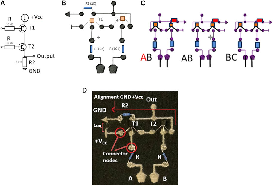
FIGURE 2. AND logic gate: (A) 2-input logic AND gate constructed using RTL resistor–transistor, (B) created embroidered digitized design for the AND logic gate, (C) structure of the AND gate cluster format, and (D) embroidered AND logic gate, detailing connector nodes and the modified GND conductive connection.
The following specific design elements had to be considered and implemented from a functionality and efficiency point of view:
• Design of input terminals A and B—connection points and the selected shape that allows additional space on the fabric panel for interconnection of the AND plane consisting of horizontal and vertical bus lines. The extended shape and size of the input connectors also allow for ease of testing and measurements.
• Due to the need to attach resistors and transistors, it is important to include embroidered connector nodes for the interconnection and placement of these components. Specific distances were selected and implemented to accommodate the components, and these distances are shown in Table 1.
• Clustering of AND gates and their interconnections was another factor that had to be considered at the single gate design level in order to ensure that they can be easily connected into a circuit. Each logic AND gate has its own GND and +Vcc connectors. Within the PLA, we have a requirement for three AND gates to be interconnected to the AND plane. Each AND gate had its own individual GND and +Vcc connections that had to be accommodated. This was a challenging aspect to consider as it involved the overlapping of various conductive circuitry thread elements that increased the risk of shorts occurring in the garment. In an attempt to limit the shorts within the overall circuit for the AND logic gate, we extended the GND connection–embroidered line so that its connection aligned in parallel with the +Vcc connection to the left-hand side, and this is illustrated in Figure 2D. The distance between the GND and +Vcc power lines is approximately 1 cm to ensure no connectivity.
• Following individual validation of the operational functionality of the embroidered AND gates, a cluster group of 3 AND gates was combined (Figure 2C), which was required for the overall circuit design.
Likewise, for the OR logic gate, the embroidery design had to accommodate 1 × 1 K resistor, 2 × 10 K resistors, and 2 × 2 × BC547B NPN transistors (T1 and T2). A similar design of input connections, conductive node connections, and placement distances (Table 1) as per the AND logic gate embroidery design was also adopted for the OR logic gate to ensure that the components fitted within the circuit’s layout as shown in Figures 3A,B.
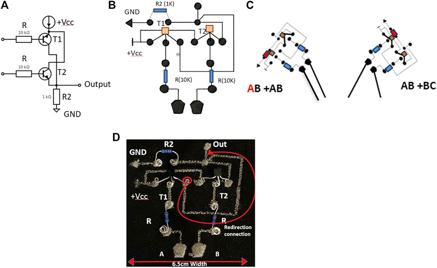
FIGURE 3. OR logic gate: (A) 2-input logic OR gate can be constructed using RTL resistor–transistor, (B) embroidered digitized design for the OR logic gate, (C) cluster of two OR gates in the PLA garment design, and (D) embroidered OR logic gate and design modifications completed in order to limit shorts from occurring.
The following additional considerations for the design were made for the OR gate:
• Due to the more complex and overlapping interconnections between the two transistors in the OR logic gate for the embroidered version, we looked at redirecting the transistor emitter–embroidered connection under the 10 K resistor and wrapped it around the edge of the T2 transistor in order to connect it to the output. This allowed us to reduce the number of overlapping wired busses and potential short circuits linked to this gate, as shown in Figure 3D.
• Completing this redirection around the 10 K resistor and the T2 transistor meant that the width of this gate was approximately 1 cm larger than that of the AND gate (Table 1).
• Redirecting the connections also allowed for the GND and +Vcc connections to be strategically placed on the left-hand side of the OR gate, allowing for ease of connection when considering the 2 OR gates in the overall PLA circuit.
• A more intricate level of connections was required to be embroidered into the OR gate. This resulted in the OR logic gate width being slightly larger than that of the AND logic gate by ∼1 cm. The OR logic gate circuit design was modified, allowing the power and ground connections to colocate on the same side, thereby increasing the efficiency and ease of the connections.
• Only two OR logic gates were required due to the defined truth table containing two outputs (Z1 and Z2). Hence, this required the replication of two OR gates to be embroidered into the top half of the garment fabric placed at approximately 45-degree angles. A 45-degree placement angle was selected in order to allow for ease of connection to the output node connection points coming from the cluster group of AND logic gates (Figure 3C).
The input connections to the PLA had the necessity to account for both the normal input and the complemented input. In order to accommodate this need in the PLA from a design perspective, we have to implement a corresponding NOT logic gate for every input. The NOT gate was constructed using RTL resistor–transistor switching as a base, as shown in Figures 4A,B.
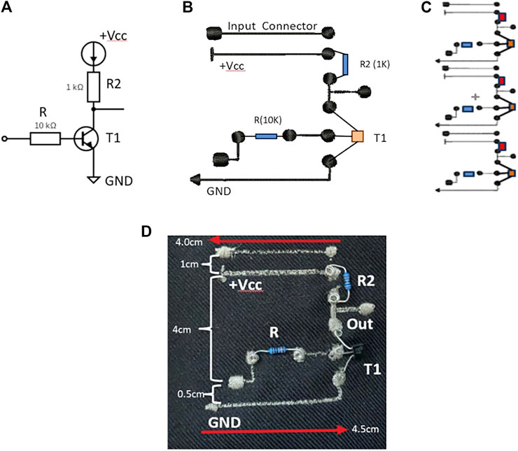
FIGURE 4. Input/inverter logic gate: (A) 2-input inverter logic gate constructed using RTL resistor–transistor, (B) inverter logic gate embroidered digitized design layout, (C) cluster of inputs (A–C) in the layout design, and (D) embroidered logic inverter and input gate detailing circuit layout measurements.
The following design requirements for the Input/NOT logic gates had to be considered:
• The normal and complemented inputs were kept separate for the sake of testing. We defined the circuit layout to have a standard input connector (e.g., representing “A” and then a set representing “complement A”). This design was taken for the other two input variables, B and C, which resulted in six input connectors that are active, as illustrated in Figure 4C.
• Each of the inverter logic gates contains GND and +Vcc connections. It was important to ensure that the layout of these connections in the garment design was considered in order to reduce any possibilities of short circuits occurring. Hence, the GND and +Vcc connections in the inverter logic gate design were extended with a longer length to accommodate the connections required.
• Standard input connections were placed vertically above the NOT gate and embroidered parallel to the +Vcc connection. The + Vcc connector and the standard input connector were 4 cm in length, and the GND connection was 4.5 cm in length. The GND connector length was slightly longer in order to allow for seamless connections between all GND connectors in the input panel, as seen in Figure 4D.
The fusion of a PLA within an e-textile environment has not been investigated previously. Taking the modular individual embroidered gates and cluster gate groupings discussed in Single Gate Model, we now have the main building blocks needed to design the required PLA. To determine the most suitable garment design configuration based on the PLA structure, we designed and developed two prototype PLA smart garments.
• Design 1: A single-layered approach where all the Inputs/NOT, AND, and OR gates coexist on one layer of fabric. This design fits the traditional PLA structures when seen from an electronic circuit design perspective.
• Design 2: A multilayered approach consisting of three layers: 1) the input/NOT logic gate plane on the outermost layer, 2) the embroidered AND gate logic plane on the middle layer, and 3) the OR gate logic plane on the inside layer closest to the human body. All three layers will be interconnected based on the defined Boolean expression and the physical overlay of the connecting programmable planes on the fabric layer.
It is important to note that when considering the fusion of the PLA into a garment structure, the following elements have to be considered from the start:
• Practical placements of the embroidered logic gate circuit structures on the garment fabric based on the physical size of the required cluster of logic gates and the location of inputs, outputs, and GND and +Vcc connections.
• Limiting the area and dimensions of the logic gates to a pragmatic size in order to be able to accommodate all the gates in a manageable format and practical layout on the fabric panel.
• PLA programmable requirements and alignments of the programmable planes which are based on the two different designs so the plane overlay can interconnect by stitching the connections.
• Durability and appearance of the garment with inbuilt embroidered PLA “on-body computing” functionality.
For the two designs, different machine-sewn planes were utilized in an attempt to analyze and compare their performance. A mixture of straight-line planes and zigzag planes were incorporated into the designs. For the single-layered design, “zigzag” stitching in a horizontal line was used for the majority of the planes, and this is illustrated in Figure 5. Each horizontal zigzag plane wired bus that was linked to an input measured approximately 14.5 cm in length. For the multilayered design, straight-line planes were used. Based on the voltage readings obtained during the validation phase along with visual assessment of the garment from a stretchability and usability point of view, the zigzag stitch type was selected as it is the most suited stitch type to use in conjunction with a lycra-based four-way stretch material.
The single-layered PLA design was selected to assess the viability of incorporating the e-textile PLA on a garment’s back panel layer of fabric. The layout of the logic gate devices was based on the criteria defined in Single Gate Model. White tailor chalk was used to mark the placement of the logic gate positions prior to hooping the fabric with tear-away interface backing in the embroidery hoop. The full circuit layout for design one can be viewed in Figure 6A.
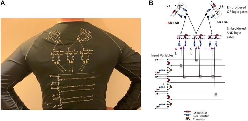
FIGURE 6. Single-layered e-textile “on the body edge worn computing” PLA garment: (A) e-textile single-layered PLA garment design and (B) single-layer embroidered circuitry overview.
From a design perspective, the cluster group of input/NOT variable connectors was placed in a vertical manner toward the lower left side of the garment. The AND logic gate cluster grouping was placed in the middle of the garment, allowing for the AND plane vertical connections (AB, AB, and BC) to be interconnected to the input/NOT plane horizontal connections shown in Figure 6B.
Outputs from the AND logic gates were connected directly to the embroidered OR logic gate inputs, allowing the final computational switching functions to occur. In order to be able to determine if an output was a high- or low-alert notification, an LED was connected to both OR gate outputs, Z1 and Z2. The OR gate output result could then be cross-compared with the initial hypertension or epilepsy health-monitoring truth table to determine the meaning of the result.
The following challenges were encountered in the initial single-layer PLA garment.
Due to each logic gate having both a GND and a +Vcc connection, it was difficult to create a logical GND and +Vcc circuit flow that could cater to all the necessary interconnections in this single-layered design. The high volume of connections between the gates and the lack of insulations also lead to many short circuits, resulting in accuracies in the logic computation.
The required interconnections from the AND gate plane to the OR gate inputs were created using individual pieces of conductive thread on fabric strips at the back of the garment, and this was not an ideal solution as the fabric connections were prone to a lot of movement and created many short circuits.
On a number of occasions, a negative flow of voltage was detected between the OR gate connections. This was most likely due to the positive side of the circuit and the negative terminal side of the circuit being connected at a point in time, altering the voltage orientation in a circuit.
Design 2 took an alternative approach of layering the modular logic gate elements of the PLA into the garment, illustrated in Figure 7, where the PLA has three planes, each containing specific types of gates that needed to be interconnected. The three layers include the following:
• Layer 1: The input/NOT logic gate plane on the outermost external layer of the garment.
• Layer 2: The AND gate logic plane housed on the middle fabric layer.
• Layer 3: The OR gate logic plane housed in the inside fabric layer closest to the human skin.
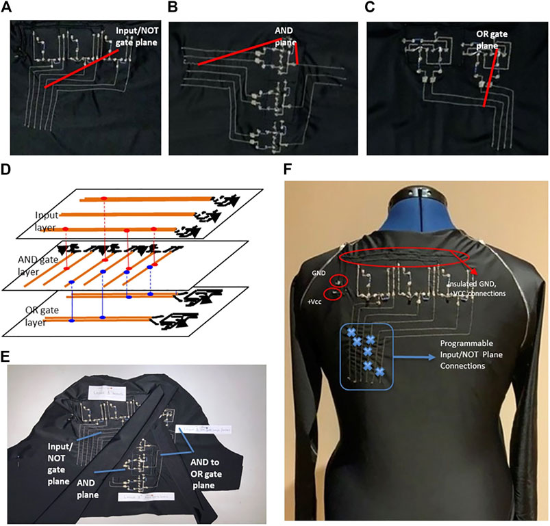
FIGURE 7. Multilayered PLA smart garment: (A) Input/NOT embroidered logic gate cluster and plane, (B) AND embroidered logic gate cluster and plane, (C) OR logic gate cluster and plane, (D) multilayered (3-layered) plane interconnected approach, (E) multilayered—three-layered fabric approach, and (F) multilayered PLA garment design.
The purpose of this three-layered design approach is to overlay the layers in a manner where we can allow for the programmable interconnections from one plane to another plane, and this is achieved by stitching the connections of the wired busses. Also, the length of the vertical/horizontal lines was decided based on the plane overlays and the most appropriate placement position on the garment in order to improve the embroidered PLA’s efficiency and voltage performance. Hence, the angle/width/direction of the plane in each layer incorporates a mixture of vertical and horizontal lines, as shown in Figures 7A–C. The planes were sewn using a “straight running machine stitch” onto specific marked sections of the three fabric layers so that they could interconnect with ease and allow for the necessary programmable stitching to be completed.
Initially, layer 1 was implemented, where the input/NOT logic gates were embroidered onto the top layer of the fabric. The input plane connections for this design were placed vertically down the left-hand side of the fabric, as shown in Figure 7A. The line lengths varied from 15 to 24 cm in length depending on the input position in the input/NOT gate logic cluster group.
Layer 2 involved planning the placement of the AND logic cluster group so that the gate inputs could interconnect and fuse to the input vertical plane connections coming from layer 1. On the right-hand side of the AND logic gates where the outputs reside, approximately 9 cm of space was allocated to include the gate’s output connection plane that was required to link to the OR logic gate plane (layer 3), as shown in Figure 7B. On the left-hand side of the AND logic gate, approximately 12 cm of space was required to be allocated in order to align the AND plane with the input plane on layer 2. A combination of vertical and horizontal lines was used to efficiently line up the planes, enabling easy stitched connection across the two layers.
Layer 3 consists of the two OR logic gates representing the outputs Z1 and Z2, as shown in Figure 7C. Layer 3 is the closest to the human skin, so we selected the cluster group with the least number of gates to reside on this layer due to the close contact with the skin. It is worth noting that for this layered approach, apart from the tear-away interface stabilizer that was used to support the embroidered gates, an iron-on fusible backing was also applied to the under-layered part of the garment. This was beneficial as it reduced the possibility of any short circuits occurring, and it was also soft to the touch, hence preventing any irritation against the skin.
Once all the individual layer planes were embroidered into the garment, the programmable connections were then sewn in to link all the layers as illustrated in Figures 7D,E, which shows the design with all the different fabric layers. Interconnections were completed using conductive thread to stitch the corresponding plane variables together as per the defined Boolean expression computed in Single Gate Model. Figure 7F shows the connections that were stitched into the embroidered PLA in order to link the modular circuit layers together.
All the +Vcc and GND connections were directed toward the left-hand side of the garment as shown in Figure 7F and is a different design from the single-layered design due to the short circuits that occurred. This was completed on all three layers, where all GND and +Vcc connections were insulated using a compressed zigzag machine stitch, as shown in Figure 8C, encapsulating the conductive thread path and preventing it from coming into contact with any other conductive elements to potentially create a short circuit in the embroidered PLA.
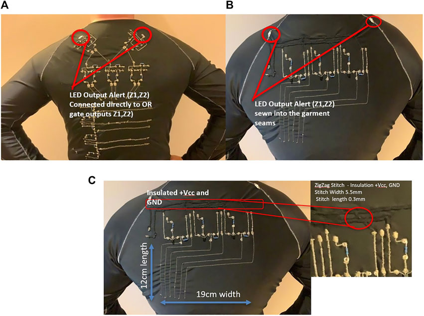
FIGURE 8. LED alert notification: (A) single-layer LED Z1 and Z2 alerts, (B) multilayer LED Z1 and Z2 alerts, and (C) +Vcc and GND connections insulated using a compressed zigzag stitch. Input/Not plane dimensions.
With all the power and GND connections located on the left-hand side of the garment, a layered connection was completed to link all three layers. This form of connection created a more solid and reliable one-point location for the battery connection.
The development of the two smart garment PLA designs provided us with the opportunity to assess the performance of each individually and also cross-compare them from an efficiency and accuracy point of view.
This section will analyze the measurement performance of the circuit by focusing on the 1) input/NOT connector plane, 2) embroidered AND logic gate, 3) embroidered OR logic gate, 4) PLA plane interconnection, and 5) comparison between the single-layered and multilayered designs.
A systematic approach was taken to initially check the workings of each logic gate on the garment of both designs before validating the PLA e-textile embroidered circuit as a whole. The key measurement was the voltage reading measurements across the circuits. For each design assessment, the input/NOT, AND, and OR embroidered logic gates were validated individually to observe their functional operations (input and output voltage readings) when power was applied to the circuit. In order to be able to determine a high-level “1” output coming from the OR logic gates, LEDs were included in the design on each PLA (Figures 8A,B). This enabled us to actively step through and validate the defined truth table variable inputs by applying the corresponding input to the PLA input connectors (A, B, and C) and assessing the outputs from the embroidered logic gates (Z1 and Z2). This section will highlight our experimental validation and analyze its outcomes.
Due to the diverse design elements incorporated into the single-layered design and the multilayered design, the input/NOT plane had varying stitching types and layout options, as detailed in Zigzag Wired Bus and Design 2: Multilayered PLA. In order to validate the computing operation of the inputs, we stepped through the truth table inputs and observed the voltage readings present at the end-most point of the input/NOT planes for both designs.
Using a standard 9 V battery to power the garment, each individual input connection was validated to ensure that the input voltage readings met the desired measurements. As can be seen from the sample input connector graphs in Figures 9A,B, there are few variations in the voltage obtained from the input/NOT connector plane in the single layer compared to the multilayered designs. On average, the input levels for the normal input connection ranged from 8.02 to 8.67 V, when the input connections to A, B, and C were in a high-level state of “1.” When the complementary input connections A, B, and C for the NOT logic gates were supplied with power, the end-plane voltage reading ranged from 0 to 0.43 V. From the tests completed, it can be concluded that due to the varying length of the planes and the different types of stitching (straight line and zigzag) used in the designs, the voltage readings showed that the stitch type used for the plane had little impact on the overall efficiency of the embroidered circuitry functional operational aspects of the garments. Purely from a practical garment design and performance point of view, seeing as there is little variation in the voltage difference, the option to use a zigzag would be the preferred design method as it allows for additional levels of movability and flexibility in the garment from a usability and wearability point of view. The zigzag stitching when stretched could expand from 14.5 to 19.5 cm on the garment. Having this expandability enables an additional level of inbuilt flexibility in the garment in order to be able to cater for varying body sizes of end users.
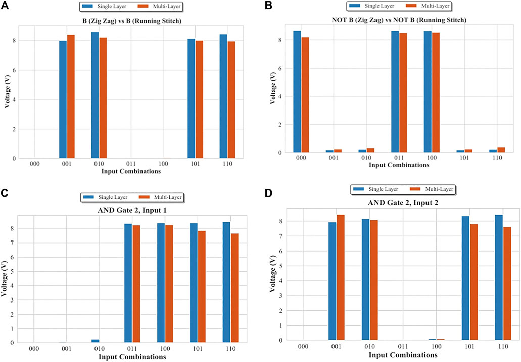
FIGURE 9. Graphs representing the voltage output reading coming from the input/NOT logic gate connectors and embroidered AND logic gate number 2 input voltage readings: (A) comparison of voltage readings from the B input connector, (B) comparison of voltage readings from the NOT B input connector, (C) AND gate 2, input 1 voltage readings, and (D) AND gate 2, input 2 voltage readings.
The cluster group of AND gates was placed in different locations depending on either the single-layered or multilayered design. The AND logic gates are central to the overall PLA, and the analysis of the voltage out of the embroidered AND logic gates is vitally important as this gives us an insight into the operational functionality of the gate. This determines if the input voltage is high enough to trigger the necessary output voltage level thresholds in order to feed into the linked embroidered OR logic gate, ensuring that the PLA operates correctly.
Voltage readings taken from the AND gate plane were analyzed based on the voltage readings at the two terminal inputs. In total, we have three individual AND gates connected to the input connection plane described in the previous subsection. Figures 9C,D provide an example of the voltage readings taken at AND gate 2 for each input based on the applied truth table input variable readings (i.e., 000–111). For both designs, only slight variations in voltage readings were detected at the AND gate input connections. This was mostly due to the variations in the input source battery supply (i.e., for a 9 V battery, after usage for various iterations of testing, its actual voltage could dip to 8–9 V). This concludes that the connections from the input/NOT connector plane to the AND connector planes on both designs worked as expected.
The voltage output readings from the AND gates demonstrate a substantial difference in the values, as shown in Figures 10A,B,C. We observed that there was a two-fold increase in the voltage levels exiting the AND gates in the multilayered design in comparison to the voltage readings coming from the single-layered design. Based on the readings obtained on average, the AND gate output for the single-layered gate had a reading of 2.7 V, whereas the multilayered AND gate output had an average high-level reading of 7.04 V. The reason for this could be linked to a number of factors that are associated with the embroidered PLA circuitry, which are listed as follows:
• In the case of the single-layered design, the AND gates are embroidered in a vertical pattern across the middle area of the garment fabric, whereas the AND gates in the multilayered design are embroidered horizontally across the middle of the fabric back panel. The layout used in the multilayered approach enables a stronger voltage reading to be emitted from the output of the three AND gates. Based on the voltage readings, we can clearly decipher that there was enhanced current flow in the multilayered AND gate cluster compared to the single-layered embroidered design.
• On the single-layered design, the AND gate cluster and layout had the GND and +Vcc connections positioned on the right side of the garment. This meant that there were connection overlays of GND and +Vcc required for the connections to the power supply. To accommodate the need for the GND and +Vcc connecting interfaces, the GND and +Vcc links were created by using conductive thread on strips of fabric in order to create the required bridge connections. This approach led to a lot of movement of the fabric strips on the inside of the garment and hence introduced random short circuits. In addition to this, the GND and +Vcc connections were not insulated, and this also led to more short circuits in the single-layered garment as opposed to the multilayered design. This in turn caused a lot of operational challenges for the cluster of AND gates within this design.
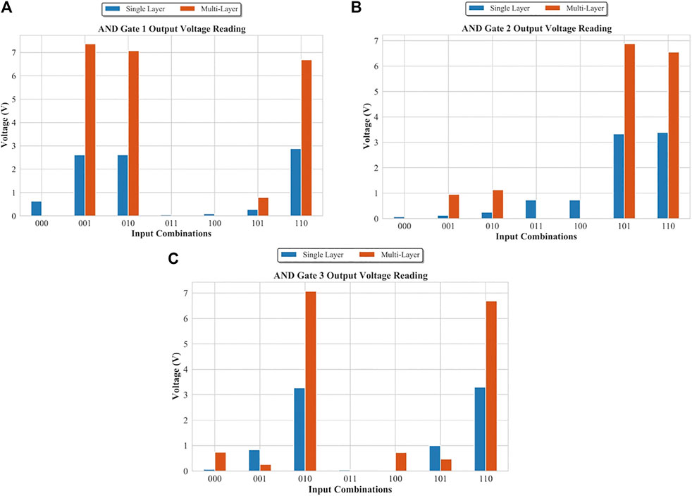
FIGURE 10. Output voltage readings of the design of single-layer and multilayer AND logic gates for (A) gate 1, (B) gate 2, and (C) gate 3.
The voltage readings coming from the AND gate plane discussed in Embroidered AND Logic Gate Validation have a direct impact on the embroidered OR gate input and output voltage readings. For the single-layered design, based on the decreased voltage readings coming from the AND logic gate outputs that were fed into the programmed OR gates based on the combinational truth table logic and Boolean expression being applied (Figure 1), there was a noticeable decrease in the output voltage levels, as shown in Figure 11. In comparison, the multilayered OR gate output readings (Z1 and Z2) were on average double in the voltage level. The voltage depletion across the AND and OR gates in the single-layered design raised challenges linked to powering additional alert notification elements connected to the OR gate output (e.g., LED). For a high-level output from the single-layered design garment, the voltage readings fluctuated between 1.91 and 2.58 V, whereas, in comparison, for the multilayered design, it fluctuated between 4.31 and 5.1 V. During testing, a noticeable LED light reduction was experienced while testing the truth table configurations to ensure that the correct outputs were being computed and achieved. The multilayered design approach with its interconnected programmable layers and insulated + Vcc and GND connections proved to be more efficient than the single-layered design.
Once all the elements were embroidered onto the fabric with the components, the next step is the stitching of the plane interconnections that represent the programmable links of our embroidered PLAs. Once this was completed, standard continuity testing was completed to
1.Ensure that the input/NOT connections (A, B, and C) were connected successfully to the inputs of the relevant AND gate connections as detailed in Figure 12C and
2.Identify and rectify any short circuits detected across the planes.
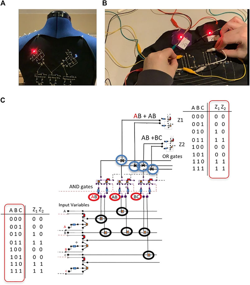
FIGURE 12. Validation of the 2 PLA smart garment designs with LED outputs, indicating a positive result of the logic circuit through OR gate outputs Z1 and Z2: (A) single-layer, (B) multilayer, and (C) programmable PLA smart garment connections.
Following this initial continuity test and validation, the PLA-embroidered fabric panels were sewn into the full garment version, and overall testing of the system was undertaken based on the defined truth table in Figure 1. This testing is based on applying the inputs to both of the garment designs’ input connectors and visually confirming if the correct alert notifications were raised, as per the defined outputs Z1 and Z2 in the truth table. This was completed multiple times across both garments, and Figures 12A,B show the LED output that will indicate a correct logic circuit output (red LED is for the Z1 output, while blue LED is for the Z2 output).
Table 3 presents the true and false output comparisons between the single- and multi-layered designs, where their meanings are described as follows:
• “True outputs” mapped to “True positive” (the outputs achieved were the correct results)
• “Indeterminate” mapped to “True negative” (the outputs obtained were the wrong results, meaning that either no LED or the wrong LED was lit up)
• “False outputs” mapped to “False positives” (this was where a short circuit was experienced, and incorrect false output results were observed).
Based on the results in Table 3, when testing multiple iterations of the single-layered logic in the garment, a large number of indeterminate output results were obtained. The reason for this is that the voltage level that was reaching the OR logic gates was not high enough to generate sufficient current to power the LED linked to the output of the OR gate. For a number of the cases where the Z1 and/or Z2 output were at high level “1,” we can see that the output voltage fluctuated between 1.7 and 2.06 V. Within the garment, this initially powered the output from the Z1 OR gate (red LED), but over time, the light intensity of the LED diminished to a level where it was difficult to read. The Z2 (blue LED) struggled to maintain any strong visible light alert throughout the tests. This again was due to the lack of current to power the LED that was coming from the OR gate. On average, the voltage levels of the output of the Z2 OR gate varied from 1.67 to 2.04 V.
Table 3 also presents the results when the single layer was stretched for 37–40 cm in the vertical direction, where the experiments were conducted based on the truth table from Figure 1. Similar challenges to the standard no-stretch tests were encountered. A number of indeterminate readings were occurring, again due to the lack of a high enough threshold voltage coming from the output of the OR gates. As this was not strong enough to power the LED and raise the visual alert notification, it hence left the test in an indeterminate state. When investigated, a number of the voltage output readings for these cases were alternating between 1.6 and 1.9 V on average.
Based on the performance results obtained when testing the multilayered design without any stretching applied, the outputs acquired were as expected, according to the defined truth table outputs of Z1 and Z2. During the tests, a few false outputs were obtained, and this was due to a small short circuit that occurred randomly on the Z2 OR gate. Upon further investigation, we found that this was due to a small piece of conductive thread that was creating a connection between the base and emitter connection nodes of the T2 transistor. This connection was generating false output readings.
When the multilayered garment undergoes stretching of 37–40 cm vertically, it was observed that the programmable interconnection stitch between the wired bus of the gates in the connector plane had become loose, and when the garment was stretched, the conductive thread stitching interacted with the circuitry in the vicinity, causing the false outputs to occur. It was also noted that the BC stitch connection of the OR gate plane also needed to be tightened to make it more secure. The movement of the garment was having an impact on the stitching interconnecting the two programmable planes. In order to overcome this in a future version, we propose to look at insulating the planes but leaving specific interconnection sites open to allow for the programming of the PLA. This would help secure the circuit and also enhance its overall performance when stretching and moving.
Overall, there were more true-positive results for the multilayered design, as shown in Table 3. In summary, the single-layered design resulted in a high level of indeterminate output results, and this is largely due to the lack of stability in this design layout.
The advancement in textiles and electronic circuitry as well as nanotechnology and material science has resulted in e-textile technologies. While the major focus of this technology to date has been on integrating sensing elements seamlessly into the garment, there is still a lack of computing capabilities that is woven into the garment. Integrating computing functionality into the garment can lead to a new form of on-body edge computing. In this study, we have presented the design, development, and validation of an e-textile embroidered PLA smart garment. This smart garment enables on-body worn edge computing capabilities, limiting dependencies on additional devices for computations. The PLA methodology allows the garment to provide a more personalized and safer approach to health monitoring at an individual level. The embroidered PLA garment is extensible to many other use cases across various sectors that include monitoring for health care or safety of a workforce. We successfully applied this PLA methodology to an e-textile fabric-based environment, leveraging embroidery techniques and conductive threads, and validated its operations. In the case of the full PLA circuitry, we initially demonstrated the design and implementation of a one-panel fabric implementation of the smart garment PLA for a single-layered design and compared this to a multilayered design. Our results showed that the multilayered design achieves more robustness in terms of the quantity of voltage that is used, as well as minimized logic computation errors compared to the single-layered design, which we found had numerous short circuits.
The main contributions of the study include 1) demonstrating the concept of programmable computing in e-textiles; 2) design and development of embroidered logic gates (AND, OR, and inverter logic gates) using graphic design layout and digitization; 3) embroidering PLA circuits into a 4-way stretch lycra fabric garment environment, enabling a programmable smart garment having the capability to stitch in and modify the connections between the wired bus planes; 4) interconnection between the embroidered logic gates using both zigzag and straight stitching wired designs to accommodate stretching and movements; 5) two different designs for the embroidered PLA that include the single- and multi-layered approaches; 6) identification of a layout (multilayered design) that can be embroidered into a garment structure and differs from the typical layouts used in standard PCB boards; and 7) validation of the PLA to measure the voltage used in the circuit and accuracy of the computation. Our proposed solution can usher in a new age of programmable on-body edge computing garments for future e-textiles that incorporate both sensing and computing. This in turn can result in new interface designs for 5G/6G wireless interfaces and applications.
The original contributions presented in the study are included in the article/Supplementary Material; further inquiries can be directed to the corresponding author.
FC, SB, and DH devised the project focus, the main conceptual ideas, and the proof outline. FC worked on the technical development elements and validation of the designs. FC, SB, and DH proposed the validation plan and contributions. FC wrote the manuscript with input from authors SB and DH.
DH and SB are funded in part by FutureNeuro from the Science Foundation Ireland (SFI) under grant number 16/RC/3948 and cofunded under the European Regional Development Fund and by FutureNeuro industry partners. SB is also funded by VistaMilk from the Science Foundation Ireland (SFI) under grant number 16/RC/3835.
The authors declare that the research was conducted in the absence of any commercial or financial relationships that could be construed as a potential conflict of interest.
We also wish to acknowledge SFI grant 15/RI/3219—“Pervasive Nation.”
Al-huda Hamdan, N., Voelker, S., Borchers, J., and Sketch, S. (2018). “Interactive Embroidery for E-Textiles”,” in Proc. Of CHI Conference on Human Factors in Computing Systems (New York, NY, USA: Association for Computing Machinery), 1–13.
Chiuchisan, I., Geman, O., and Hagan, M. (2019). “Wearable Sensors in Intelligent Clothing for Human Activity Monitoring,” in Proc. Of International Conference on Sensing and Instrumentation in IoT Era (ISSI) (Lisbon, Portugal: IEEE Sensors Journal), 1–4.
Dubé, C. M., Brewster, A. L., and Baram, T. Z. (2009). Febrile Seizures: Mechanisms and Relationship to Epilepsy. Brain Dev. 31 (5), 366–371. doi:10.1016/j.braindev.2008.11.010
Fernández-Caramés, T., and Fraga-Lamas, P. (2018). Towards the Internet-Of-Smart-Clothing: A Review on IoT Wearables and Garments for Creating Intelligent Connected E-Textiles. Electronics 7 (12), 405. doi:10.3390/electronics7120405
Fuchs, F. D., and Whelton, P. K. (2020). High Blood Pressure and Cardiovascular Disease. Hypertension 75, 285–292. doi:10.1161/hypertensionaha.119.14240
Gonçalves, C., Ferreira da Silva, A., Gomes, J., and Simoes, R. (2018). Wearable E-Textile Technologies: A Review on Sensors, Actuators and Control Elements. Inventions 14 (1), 3. doi:10.3390/inventions3010014
Hassan, N., Yau, K.-L. A., and Wu, C. (2019). Edge Computing in 5G: A Review. IEEE Access 7, 127276–127289. doi:10.1109/access.2019.2938534
Ismar, E., Kurşun Bahadir, S., Kalaoglu, F., and Koncar, V. (2020). Futuristic Clothes: Electronic Textiles and Wearable Technologies. Glob. Challenges 4, 1900092. doi:10.1002/gch2.201900092
Kubicek, J., Fiedorova, K., Vilimek, D., Cerny, M., Penhaker, M., Janura, M., et al. (2020). “Recent Trends, Construction and Applications of Smart Textiles and Clothing for Monitoring of Health Activity: A Comprehensive Multidisciplinary Review,” in IEEE Reviews in Biomedical Engineering (New York, NY: Early Access).
Lugoda, P., Hughes-Riley, T., Oliveira, C., Morris, R., and Dias, T. (2018). Developing Novel Temperature Sensing Garments for Health Monitoring Applications. Fibers 6 (3), 46. doi:10.3390/fib6030046
Mecnika, V., Hoerr, M., Krievins, I., Jockenhoevel, S., and Gries, T. (2015). Technical Embroidery for Smart Textiles: Review. Riga, Latvia: Materials Science. Textile and Clothing Technology, 9.
Parvinzadeh Gashti, M., Pakdel, E., and Alimohammadi, F. (2016). “Nanotechnology-based Coating Techniques for Smart Textiles,” in Active Coatings for Smart Textiles (New York, NY, USA: Elsevier), 243–268. doi:10.1016/b978-0-08-100263-6.00011-3
Ramasamy, S., and Balan, A. (2018). Wearable Sensors for ECG Measurement: a Review. Sr 38 (4), 412–419. doi:10.1108/sr-06-2017-0110
Szelényi, Z., and Komoly, S. (2018). Thermoregulation: From Basic Neuroscience to Clinical Neurology, Part 2. Temperature 6, 7–10. doi:10.1080/23328940.2018.1541680
Yang, K., Isaia, B., Brown, L., and Beeby, S. (2019). E-textiles for Healthy Ageing. Sensors 20 (19), 4463. doi:10.3390/s19204463
Keywords: e-textiles, PLA, embroidered logic, on-body edge computing, wearable, user interaction
Citation: Cleary F, Henshall DC and Balasubramaniam S (2021) On-Body Edge Computing Through E-Textile Programmable Logic Array. Front. Comms. Net 2:688419. doi: 10.3389/frcmn.2021.688419
Received: 30 March 2021; Accepted: 20 May 2021;
Published: 11 June 2021.
Edited by:
Nasir Saeed, National University of Technology, PakistanReviewed by:
Jooyong Kim, Soongsil University, South KoreaCopyright © 2021 Cleary, Henshall and Balasubramaniam. This is an open-access article distributed under the terms of the Creative Commons Attribution License (CC BY). The use, distribution or reproduction in other forums is permitted, provided the original author(s) and the copyright owner(s) are credited and that the original publication in this journal is cited, in accordance with accepted academic practice. No use, distribution or reproduction is permitted which does not comply with these terms.
*Correspondence: Frances Cleary, RnJhbmNlcy5DbGVhcnlAd2FsdG9uaW5zdGl0dXRlLmll
Disclaimer: All claims expressed in this article are solely those of the authors and do not necessarily represent those of their affiliated organizations, or those of the publisher, the editors and the reviewers. Any product that may be evaluated in this article or claim that may be made by its manufacturer is not guaranteed or endorsed by the publisher.
Research integrity at Frontiers

Learn more about the work of our research integrity team to safeguard the quality of each article we publish.