
94% of researchers rate our articles as excellent or good
Learn more about the work of our research integrity team to safeguard the quality of each article we publish.
Find out more
ORIGINAL RESEARCH article
Front. Phys. , 16 August 2024
Sec. Optics and Photonics
Volume 12 - 2024 | https://doi.org/10.3389/fphy.2024.1447997
 Gebru Tesfaye Sherka*
 Habte Dulla Berry*
Because of their quantum confinement effects and adjustable features, semiconductor nanoparticles have attracted a lot of attention for their various uses in optoelectronic devices. This study investigates how size and shape variations affect the optoelectronic properties of semiconductor nanoparticles InX (X = As, Sb, and P). Using unified thermodynamics modeling, it explores the effects of these nanoparticles’ diameters on their electronic band structures, optical properties, and charge carrier dynamics. The inquiry focuses on InX nanoparticles with different sizes and nanostructure morphologies. By examining electronic band structures, the density of states, and optical absorption spectra, the size-dependent quantum confinement processes that govern the optical band gap transitions and excitonic behaviors in these semiconductor nanoparticles were made clear. Also, the influence of the shape of the nanoparticles on carrier mobility and electronic band alignment is investigated, offering insights into the possibility of controlling the morphology to customize optoelectronic capabilities. This theoretical analysis indicates that altering the optoelectronic properties of InX semiconductor nanoparticles is mostly dependent on their size and shape. Smaller nanoparticles show stronger quantum size effects, which lead to improved exciton confinement and blue shifts in the optical absorption spectra. Shape-dependent differences in the density of states and electronic band structures indicate the impact of morphology on the dynamics and recombination of charge carriers in the nanoparticles. In conclusion, this work provides important insights for the design and optimization of semiconductor nanomaterials for photovoltaic, sensing, and light-emitting applications by thoroughly examining the impact of size and shape on the optoelectronic properties of InX semiconductor nanoparticles.
In the field of semiconductor physics, there has been a notable and significant trend that involves the convergence of physics, materials sciences, and technology. Researchers are actively involved in creating complicated structures and composites that possess distinct and exceptional physical properties [1]. Complex structures in the field of semiconductor physics cover a range of fascinating examples, among which nanometer-sized semiconductor crystallites stand out as an important subset [2]. Established that they have interfaces or grain boundaries, nanomaterials are combinations of nanocrystals. Due to their high surface-to-volume ratio and quantum effect, these materials have unique properties. When systems are at the nanoscale, where there are more atoms on the surface, quantum confinement effects are predominant in their electrical and optical properties [3]. Semiconductor nanostructures display size-dependent electrical and optical properties due to quantum confinement effects. At the nanoscale, materials exhibit higher surface-to-volume ratios and quantum effects compared to bulk materials, increasing surface impacts that are typically insignificant in bulk materials. These nanosolids contain free carriers due to their reduced volume, allowing the observation of quantum phenomena that are unattainable in larger bulk materials. Because of quantum confinement, the band gap of semiconductor nanomaterials can be adjusted according to the size of the nanomaterial [4–6]. This holds substantial significance for prospective uses such as solar cells [7], light-emitting diodes [8], optoelectronic devices [9], and biological labeling [10]. Scientists are not only driven by fundamental notice in studying nanosolids but also by the potential technological innovations these materials offer. The shape and size of nanoparticles play a crucial role in influencing the thermophysical and electro-optical properties of nanomaterials [11–15].
Many studies have explored the correlation between the size of nanosolids and their properties [16–25]. However, a lack of consistent understanding persists regarding how the properties of nanostructured solids are influenced by their size and shape. Guisbiers et al. [16] presented the effect of shape and size on the energy band gap and melting temperature of TiO2 nanostructure using the thermodynamic method. A size-dependent cohesive energy model has been used to estimate the size-dependent valence and conduction band gap of semiconductor nanosolids [17]. A method of tuning the band gap within the quantum confinement regime may be possible thanks to the individual diamond nanocrystals’ form, as demonstrated by the electronic structure simulation [26]. According to Liang et al.’s size-dependent phonon frequency report for TiO2, Si, and InP, the frequency shifts with decreasing crystal size based on size-dependent force constant, bond length, and bond energy [27].
The size-dependent dielectric constant in theory and experiment has attracted much attention [28–30]. The importance of dielectric properties for materials destined for nanotechnology is growing. As they characterize the ion and electron mobility response to the dipole displacement in an externally applied field, dielectric constants are closely associated with materials’ conductivity and optical properties. Because the dielectric constant affects the Coulomb interaction between electrons, which in turn affects the activation (electron-hole pair) energies, changes to it would have a significant impact on the optical absorption and transport characteristics of semiconductor devices [31]. Capacitors, electronic memories, and optical filters have all been made using improved dielectric characteristics. According to M. Singh et al.'s bond theory model, the size and shape-dependent properties of semiconductor nano solids TiO2, CdS, CdSe, Si, and GaN have theoretically been described. These properties include band gap, dielectric constant, and phonon frequency [18]. This study focuses on exploring the optoelectronic properties of InX (X = As, Sb, P) zinc blend semiconductor nanoparticles. These materials are essential for semiconductor nanotechnology because of their unique properties, and potential applications, which include high electron mobility, narrow band gaps, spintronics potential, and application versatility. Their ongoing research opportunities position them as essential components in the realm of semiconductor nanotechnology [32, 33].
In this study, we modified the Qi and Wang Model to evaluate the size and shape-dependent optoelectronic properties of InX (X = As, Sb, P) Semiconductor Nanosolids, including the dielectric constant, phonon frequency, electrical susceptibility, and band gap, taking into account the packing factor, surface effect, and bond theory. The basic is used for the spherical, tetrahedral, hexagonal, and octahedral semiconductor nano solids InX (X = As, Sb, and P). The simulated data compared with the experimental result, previously reported data, and other theoretical modeling are presented in a graph. The graphs show that phonon frequency, electrical susceptibility, and dielectric constant decrease, reducing the size and changing the shape of nanostructures but these can lead to increasing the band gap at the nanoscale scale. Our model can be used as a forecasting tool to find the dielectric constant, phonon frequency, electrical susceptibility, and the energy band gap of semiconducting nanoparticles in the lack of experimental data.
Quantum confinement effects become significant in nanoparticles when their dimensions shrink below a critical threshold. This is due to the extremely small size of the nanoparticle. The critical size is determined by the Exciton Bohr diameter, a property that is specific to each material. This diameter can vary significantly, ranging from 1 nm to over 100 nm. When the size of a semiconductor nanocrystal approaches the exciton Bohr radius, the confinement of charge carriers leads to an increase in their energy levels. This results in a widening of the band gap energy, particularly impacting optoelectronic properties.
The Qi and Wang model has proven effective in analyzing a wide range of materials, encompassing semiconductors, ceramics, and nanomaterials. However, it is important to remember that the model relies on the assumption of a uniform, isotropic solid without any structural defects [18, 22, 23, 34]. The cohesive energy of nanosolids is determined by adding the contributions of the atoms in the inner and outer shells, as per the bond energy model. As Qi and Wang Model [35], the cohesive energy of nanomaterials
here,
The melting temperature of bulk material
here,
here,
When accounting for variations in particle shape, the shape factor
here,
The total number of surface atoms,
The number of total atoms of nano solid is the ratio of the particle volume to the atomic volume, which may be written as
Because the volume of the nano solid is the same as the volume of the atom, the atom is an ideal sphere.
To precisely calculate the number of total atoms within a nanoparticle, the packing factor (
The packing factor (μ), which is defined as follows, establishes the maximum percentage of the available volume that may be filled with hard spheres [38]:
Combining Equations 7, 9, the ratio of the total number of surface atoms to the number of total atoms within a nanoparticle becomes;
Now, substituting Equation 11 into Equation 1, then Equation 1 gives the size and shape-dependent cohesive energy of nano solids containing the packing factor
Equation 12 also gives the size and shape-dependent melting temperature of nano solids containing the packing factor
As the size of the nanocrystals gets smaller, the Raman frequency in semiconductors decreases [39]. The relationship between the vibrational frequency of electrons in solid atoms and the square root of cohesive energy can be used to ascertain the impact of size on the vibrational frequency of electrons in semiconductor nanomaterials [40]. Thus, the vibrational frequency of electrons in bulk material
Substituting Equation 12 into Equation 14, the relation becomes;
The expression for electrical conductivity
here,
here,
The size-dependent activation energy is the difference between the energy of the conduction band (EC) and the energy at the fermi level (EF). Thus,
To obtain the size and shape-dependent band gap of nanomaterial, substituting Equation 13 into Equation 19 and rewritten as;
Electrical susceptibility
A dimensionless number known as electrical susceptibility relates to a material’s band gap by indicating the degree of polarization of the dielectric substance. The approximate relationship between the band gap
here,
here,
Here,
Now, substituting Equation 20 into Equation 24, the size and shape-dependent dielectric constant can be rewritten as;
According to Equations 20, 23 the electrical susceptibility for semiconducting nanomaterials can be calculated as;
The expression in Equation 26 presents the electrical susceptibility of semiconducting nanomaterials depending on their size and shape.
Equations 15, 20, 25, 26 describe models that rely on the sizes and shapes of nanoscale solids. These equations establish connections for the frequency of phonons, the band gap, the dielectric constant, and the electrical susceptibility of nanoscale solids, respectively, considering the crystal’s packing efficiency.
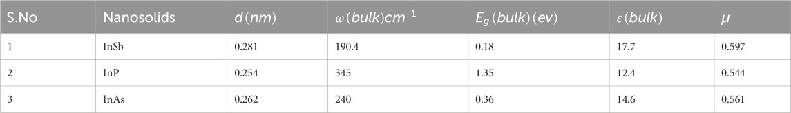
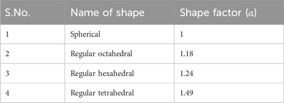
Research on the impact of size and shape on the optoelectronic properties of semiconductor nanoparticles reveals intriguing insights into the quantum confinement effects and morphology-induced variations in the electronic and optical behaviors of these nanostructures. To validate the accuracy of our model regarding variations in phonon frequency, variations in band gap, changes in dielectric constant, and fluctuations in electrical susceptibility, we have selected direct band gap semiconductor materials from group III-V, specifically InX (where X represents As, Sb, or P). The phonon frequency, bandgap, dielectric constant, and electrical susceptibility of InX (X = As, Sb, P) semiconductor nanoparticles are analyzed as a function of their size and shape using specific equations. Equations 15, 20, 25, 26 are employed to study the variations in these properties for nanoparticles with spherical, tetrahedral, hexagonal, and octahedral shapes, respectively. The input parameters are presented in Tables 1, 2. Figures 1–12 illustrate the variations in phonon frequency, bandgap, dielectric constant, and electrical susceptibility as a function of size for InX (where X is As, Sb, or P) semiconductor nanoparticles, along with available experimental and simulation data. Also, for covalent bonding and the zinc blend structure, it also provides a pre-calculated packing factor (μ) using the formula in Equation 10. Atoms within nanosolids can occupy various positions. In one scenario, an atom may be situated such that one-fourth of its volume is within the nanosolid, while three-fourths extends into a vacuum. Consequently, the relaxation factor is set at 0.75, indicating a surface atom that relaxes towards the vacuum [45]. The relaxation factor is set to 0.75, indicating that surface atoms relax towards the vacuum [46].
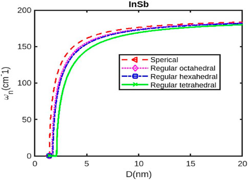
Figure 1. The variation of the phonon frequency with the size of the InSb nanoparticle.
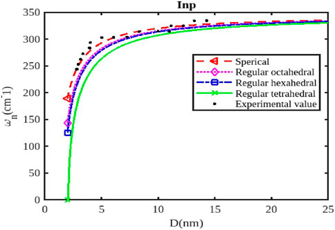
Figure 2. The variation of the phonon frequency with the size of the InP nanoparticle. The experimental data are taken from [47, 48].
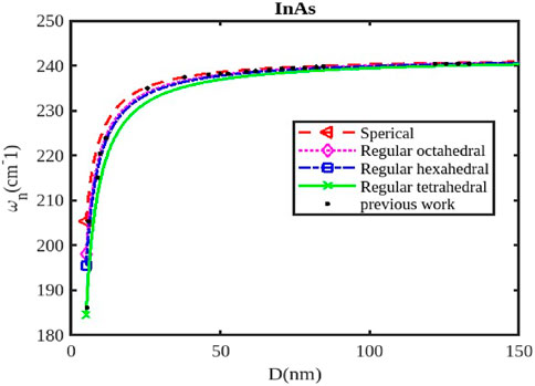
Figure 3. The variation of the phonon frequency with the size of the InAs nanoparticle. The previous work was reported in Ref. [47].
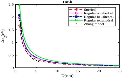
Figure 4. The band gap variation with the size of the InSb nanoparticle. The Zhang model was reported in Ref. [54].
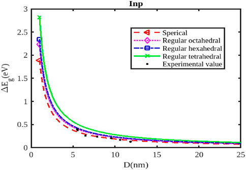
Figure 5. The variation of the band gap with the size of the InP nanoparticle. The experimental data are taken from [55].
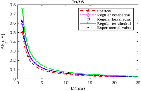
Figure 6. The variation of the band gap with the size of the InAs nanoparticle. The experimental data are taken from [56].
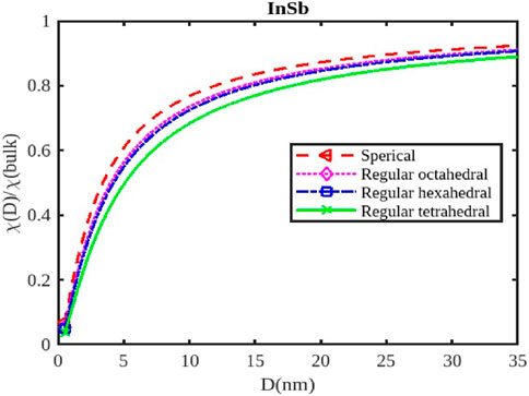
Figure 7. The variation of the electrical susceptibility with the size of the InSb nanoparticle.
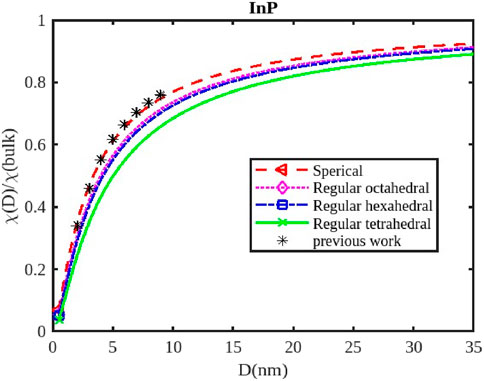
Figure 8. The variation of the electrical susceptibility with the size of the InP nanoparticle. The previous work was reported in Ref. [3].
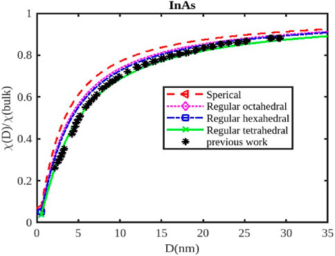
Figure 9. The variation of the electrical susceptibility with the size of the InAs nanoparticle. The previous work was reported in Ref. [3].
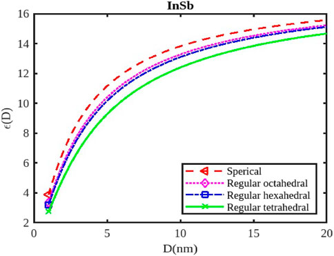
Figure 10. The variation of the dielectric constant with the size of the InSb nanoparticle.
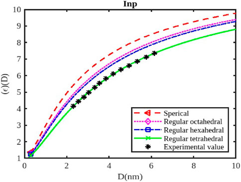
Figure 11. The variation of the dielectric constant with the size of the InP nanoparticle. The experimental data are taken from [57].
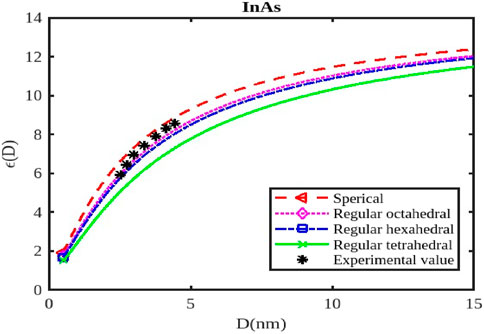
Figure 12. The variation of the dielectric constant with the size of the InAs nanoparticle. The experimental data are taken from [57].
The size and shape of InX (X = As, Sb, P) nanoparticles significantly affect their phonon frequencies, influencing their thermal properties, vibrational modes, and interactions with light. As nanoparticle size decreases, the surface-to-volume ratio increases, leading to a greater contribution from surface phonons. These surface modes have lower frequencies compared to bulk phonons (Figures 1–3), affecting the overall phonon spectrum. Quantum confinement effects in smaller nanoparticles can alter the vibrational modes and phonon frequencies due to the restricted movement of atoms within the confined space. This can lead to shifts in phonon frequencies and changes in the overall phonon spectrum. The density of states for phonons can change with size, influencing the specific phonon frequencies and the intensity of vibrational modes. When the size of semiconductor nanocrystals falls below 5 nm, which is comparable to the exciton radius, the confinement effect becomes significantly stronger, leading to a rapid decline in phonon frequency, as illustrated in Figures 1, 2.
Different shapes (Figures 1–3) of nanoparticles exhibit anisotropic phonon properties, meaning their vibrational modes and frequencies vary depending on the direction of propagation. This anisotropy arises from the unique geometry and symmetry of different shapes. The specific morphology of the surface (e.g., corners, edges, facets) can affect the vibrational modes and phonon frequencies by influencing the local atomic arrangement and interactions. The phonon frequencies of InX nanoparticles are also influenced by the specific material (InAs, InSb, or InP), as each material has distinct atomic masses and bonding strengths. Figures 1–3 illustrate the relative changes in phonon frequency for InAs, InSb, and InP nanosolids across various sizes and shapes. It is clear that for the same particle size, the order of phonon frequency size effects, from strongest to weakest, is as follows: spherical, octahedral, hexahedral, and tetrahedral. This indicates that the confinement effects are more significant in spherical shapes compared to tetrahedral, hexahedral, and octahedral shapes. Figure 2 illustrates the impact of shape and size on the variation of phonon frequency for InP nanosolids, comparing spherical, octahedral, hexagonal, and tetrahedral shapes, along with available experimental data [47, 48]. It has been observed that the phonon frequency, denoted as
Surface passivation can alter the phonon frequencies by modifying the surface chemistry and reducing surface defects. Strain introduced by the size or shape of the nanoparticle can lead to shifts in phonon frequencies and changes in the phonon spectrum. The phonon frequencies of InX nanoparticles can influence their thermal conductivity and heat dissipation properties, impacting their use in thermal management applications. Changes in phonon frequencies due to size and shape can be observed using Raman spectroscopy, providing a powerful tool for characterizing and understanding the properties of nanoparticles. Phonon properties can affect the efficiency and performance of optoelectronic devices like LEDs and solar cells by influencing electron-phonon interactions and heat dissipation.
The band gap energy of InX (X = As, Sb, P) semiconductor nanoparticles is a fascinating area of research with significant implications for optoelectronic applications. Our computations, along with existing experimental and theoretical models for the energy gap
As the size of the InX nanoparticles decreases, the electrons are confined within a smaller space, leading to a phenomenon called quantum confinement. This confinement quantizes the energy levels of the electrons, resulting in a wider band gap (Figures 4–6). The widening of the band gap due to quantum confinement leads to a blue shift in the optical absorption spectrum. This means that smaller nanoparticles absorb higher-energy (shorter wavelength) light, while larger nanoparticles absorb lower-energy (longer wavelength) light. Overall, the energy band gap for semiconductor nanoparticles increases with decreasing size. This significant increase in the band gap allows for tuning the optical properties of semiconductor nanoparticles for applications like infrared detectors or solar cells.
Different shapes of nanoparticles (Figures 4–6), such as spherical shapes exhibit different degrees of quantum confinement along specific directions. This leads to anisotropic band gaps, where the band gap energy varies depending on the direction of light absorption or emission. By controlling the shape of InX nanoparticles, researchers can precisely tune the band gap energy, tailoring the material’s optical properties for specific applications. Size and shape are not independent parameters. The shape of a nanoparticle can influence its effective size and, in turn, the degree of quantum confinement.
The specific size and shape effects vary depending on the InX material (InAs, InSb, or InP). Understanding the size and shape effects on the band gap of InX nanoparticles allows researchers to design and synthesize these materials with specific optical properties for a wide range of applications. By tailoring the band gap of InX nanoparticles, researchers can optimize solar cell efficiency by maximizing light absorption. The size-dependent band gap allows for tuning the wavelength sensitivity of photodetectors, making them suitable for specific applications like infrared detection. The anisotropic band gap in shaped nanoparticles can be utilized to develop LEDs with polarized light emission. This exploration of the size and shape effects on the band gap energy of InX nanoparticles highlights the tremendous potential of these materials for advancing optoelectronic technologies. Slight variations in the experimental data underscore the necessity for a deeper understanding to fully interpret them. Nonetheless, it has been observed that a consistent trend of band gap expansion occurs for the selected compounds as the particle size decreases. Our model, which simultaneously considers voids in the crystal structure, dangling surface atoms, and the shape of the material, is supported by this observation. Consequently, the packing factor, size, and shape of a semiconductor nanomaterial influence the expansion of its band gap.
For InX (X = As, Sb, P) III-V semiconductor nanoparticles, the size dependence of electrical susceptibility has been calculated using Equation 26 for spherical, octahedral, hexahedral, and tetrahedral shapes. Figures 7–9 graphically depict the computed results for the size and shape dependency of the electrical susceptibility of the InSb, InP, and InAs semiconductor nanomaterials respectively, along with the data from other existing theories. The graphs indicate that electrical susceptibility reduces as the particle size decreases. At a given particle size D, the variation of the electrical susceptibility follows the order:
The electrical susceptibility of InX (X = As, Sb, P) nanoparticles is significantly influenced by their size and shape, impacting their response to external stimuli like magnetic fields and electric fields. As nanoparticles shrink in size, their surface-to-volume ratio increases dramatically (Figures 7–9). This means a larger proportion of atoms reside on the surface, leading to; increased surface reactivity: Nanoparticles exhibit higher reactivity due to their increased surface area, making them more electrically susceptible to interactions with the environment, surface passivation: Surface passivation strategies are crucial for stabilizing nanoparticles and minimizing their reactivity, which can significantly influence their electrical susceptibility, quantum Confinement: Quantum confinement effects in smaller nanoparticles (Figures 7–9) can alter their electronic structure and energy levels, affecting their response to external fields.
Different shapes of nanoparticles exhibit anisotropic properties, meaning their behavior varies depending on the direction of the applied field. For instance; Electric Susceptibility-Shape anisotropy can also lead to different responses to electric fields, affecting their dielectric properties and polarizability, Surface Morphology- The specific morphology of the surface (e.g., corners, edges, facets) can further influence the susceptibility of nanoparticles by affecting their surface charge distribution and interaction with external fields. The susceptibility of InX nanoparticles is influenced by the specific material (InAs, InSb, or InP), as each material has distinct electronic and magnetic properties. Understanding the size and shape effects on susceptibility is critical for designing nanoparticles with tailored properties for magnetic resonance imaging (MRI) applications, drug delivery, sensors, and more. InX nanoparticles can be engineered to enhance contrast in MRI imaging, improving diagnostic capabilities. Their susceptibility can be tuned by controlling their size and shape to optimize their interaction with the magnetic field. By manipulating the magnetic susceptibility of nanoparticles, they can be directed to specific locations within the body for targeted drug delivery or therapy. Changes in the susceptibility of InX nanoparticles due to external stimuli can be used to detect changes in the environment, creating sensitive sensors for various applications.
The calculations of the dielectric constants are stated in Figures 10–12 by Equation 25 for the InSb, InP, and InAs semiconductor nanostructured materials at the nanoscale. The variations in the dielectric constant for InSb nanomaterial in different shapes; spherical, octahedral, hexahedral, and tetrahedral are illustrated in Figure 10, along with their size dependencies. The figure illustrates that the relative change in the dielectric constant initially starting from its bulk dielectric constant decreases gradually and then drops sharply as the particle size reduces. To verify our model for InSb the experimental data is not available in the works of literature. The variations of the dielectric constant of InP nanosolid have been calculated by Equation 25 and results are projected along with the available experimental data as shown in Figure 11 for tetrahedral [57]. It is observed that
The dielectric constant of InX (X = As, Sb, P) nanoparticles is significantly affected by their size and shape, influencing their response to electric fields and their potential for various applications like capacitors, sensors, and optoelectronic devices. As nanoparticles shrink, quantum confinement effects become prominent, altering the electronic energy levels and, consequently, the dielectric constant. Smaller nanoparticles generally exhibit higher dielectric constants (Figures 10–12) due to increased electronic polarizability resulting from quantum confinement. This enhanced polarizability arises from the greater confinement of electrons, allowing them to respond more readily to applied electric fields. The dielectric constant typically increases as the particle size decreases, reaching a maximum value at a certain critical size. Beyond this point, the dielectric constant might decrease again due to surface effects or other factors.
Different shapes of nanoparticles exhibit anisotropic dielectric properties, meaning their response to electric fields varies depending on the direction of the applied field. This anisotropy can be exploited to create materials with specific dielectric properties for applications like capacitors or sensors. The surface morphology of nanoparticles (e.g., corners, edges, facets) can significantly influence their dielectric constant due to changes in surface charge distribution and interactions with the electric field. The dielectric constant of InX nanoparticles is also influenced by the specific material (InAs, InSb, or InP), as each material has distinct electronic properties. Surface passivation strategies can significantly impact the dielectric constant of nanoparticles by reducing surface defects and modifying their interactions with the environment. External factors like temperature, pressure, and the presence of other materials can influence the dielectric constant of nanoparticles. By tuning the size and shape of InX nanoparticles, researchers can create materials with significantly higher dielectric constants than bulk materials, suitable for high-performance capacitors. Changes in the dielectric constant of InX nanoparticles due to external stimuli (temperature, pressure, or chemical exposure) can be used to develop sensitive sensors for various applications. The dielectric constant plays a crucial role in the performance of optoelectronic devices like LEDs and solar cells. By controlling the dielectric properties of InX nanoparticles, researchers can optimize the efficiency and functionality of these devices.
This research introduces a unified model that can accurately predict the phonon frequency, energy band gap, electrical susceptibility, and dielectric constant of InSb, InP, and InAs semiconductor nanoparticles. The model takes into account the varying shapes, sizes, packing efficiency, and relaxation factor of these nanoparticles, providing a deeper understanding of their electronic and optical properties. Our findings demonstrate a correlation between the size and shape of semiconductor nanoparticles and their optoelectronic properties. As the nanoparticles shrink, their band gap widens, while the phonon frequency, electrical susceptibility, and dielectric constant decrease. Additionally, deviations from a spherical shape result in a greater expansion band gap at the nanoscale, but minimum reduction of the phonon frequency, electrical susceptibility, and dielectric constant. Thus, taking into account different shapes and size ranges that have not been previously studied, this comprehensive model may be utilized to analyze the differences in the phonon frequency, band gap, electrical susceptibility, and dielectric constant of distinct semiconductor nanoparticles.
The conclusions drawn from this study shed light on the significance of size and shape engineering in tailoring the electronic and optical characteristics of these semiconductor nanoparticles. The size and shape of InX nanoparticles play a crucial role in determining their susceptibility. This knowledge is essential for designing and tailoring nanoparticles for specific applications that leverage their unique properties for advancing fields like medical imaging, drug delivery, and sensing. The size and shape of InX nanoparticles exert significant influence on their dielectric constant, offering a powerful tool for tailoring these materials for a wide range of applications. This understanding paves the way for developing novel materials with enhanced dielectric properties. The size and shape of InX nanoparticles significantly impact their phonon frequencies, leading to changes in their thermal properties, vibrational modes, and interactions with light. This understanding is crucial for tailoring these materials for various applications in thermal management, sensing, and optoelectronics, as well as energy storage, sensing, and optoelectronic applications.
Future research directions may involve exploring the combined effects of size, shape, and composition on the electrical susceptibility and dielectric constant of In (X = As, Sb, P) nanoparticles. Additionally, the investigation of novel synthesis techniques to achieve precise control over the size and shape of these nanoparticles will be essential for advancing their applications in cutting-edge technologies. In summary, the variation of electrical susceptibility and dielectric constant with size and shape in In (X = As, Sb, P) nanoparticles highlights the importance of these parameters in understanding and tailoring the electrical properties of nanomaterials. By harnessing the size- and shape-dependent effects, researchers can unlock new possibilities for designing and utilizing In (X = As, Sb, P) nanoparticles in advanced electronic and optoelectronic applications.
The original contributions presented in the study are included in the article/supplementary material, further inquiries can be directed to the corresponding authors.
GS: Conceptualization, Data curation, Formal Analysis, Investigation, Methodology, Software, Validation, Visualization, Writing–original draft, Writing–review and editing. HB: Conceptualization, Formal Analysis, Investigation, Methodology, Supervision, Validation, Writing–review and editing.
The author(s) declare that no financial support was received for the research, authorship, and/or publication of this article.
The authors declare that the research was conducted in the absence of any commercial or financial relationships that could be construed as a potential conflict of interest.
All claims expressed in this article are solely those of the authors and do not necessarily represent those of their affiliated organizations, or those of the publisher, the editors and the reviewers. Any product that may be evaluated in this article, or claim that may be made by its manufacturer, is not guaranteed or endorsed by the publisher.
1. Lindl JD, McCrory RL, Campbell EM. Progress toward ignition and burn propagation in inertial confinement fusion. Phys Today (1992) 45(9):32–40. doi:10.1063/1.881318
3. Pachauri U, Joshi DP, Arora N. Theoretical model for size, dimension and shape effect on electrical behavior of semiconductor nanomaterials. Appl Phys A (2020) 126:253–11. doi:10.1007/s00339-020-3411-1
4. Hu H, Zhang W. Synthesis and properties of transition metals and rare-earth metals doped ZnS nanoparticles. Opt Mater (Amst) (2006) 28(5):536–50. doi:10.1016/j.optmat.2005.03.015
5. Brus L. Electronic wave functions in semiconductor clusters: experiment and theory. J Phys Chem (1986) 90(12):2555–60. doi:10.1021/j100403a003
6. Rossetti R, Hull R, Gibson JM, Brus LE. Excited electronic states and optical spectra of ZnS and CdS crystallites in the≊ 15 to 50 Å size range: evolution from molecular to bulk semiconducting properties. J Chem Phys (1985) 82(1):552–9. doi:10.1063/1.448727
8. Coe S, Woo W-K, Bawendi M, Bulović V. Electroluminescence from single monolayers of nanocrystals in molecular organic devices. Nature (2002) 420(6917):800–3. doi:10.1038/nature01217
9. Duan X, Huang Y, Agarwal R, Lieber CM. Single-nanowire electrically driven lasers. Nature (2003) 421(6920):241–5. doi:10.1038/nature01353
10. Zhang H, Wang L, Xiong H, Hu L, Yang B, Li W. Hydrothermal synthesis for high-quality CdTe nanocrystals. Adv Mater (2003) 15(20):1712–5. doi:10.1002/adma.200305653
11. Tan OK, Zhu W, Yan Q, Kong LB. Size effect and gas sensing characteristics of nanocrystalline xSnO2-(1−x) α-Fe2O3 ethanol sensors. Sensors Actuators B Chem (2000) 65(1–3):361–5.
12. Campbell CT, Parker SC, Starr DE. The effect of size-dependent nanoparticle energetics on catalyst sintering. Science (80) (2002) 298(5594):811–4. doi:10.1126/science.1075094
13. Christenson HK. Confinement effects on freezing and melting. J Phys Condens Matter (2001) 13(11):R95–R133. doi:10.1088/0953-8984/13/11/201
14. Veprek S, Argon AS. Towards the understanding of mechanical properties of super-and ultrahard nanocomposites. J Vac Sci Technol B Microelectron Nanom Struct Process Meas Phenom (2002) 20(2):650–64. doi:10.1116/1.1459722
15. Tersoff J, Ruoff RS. Structural properties of a carbon-nanotube crystal. Phys Rev Lett (1994) 73(5):676–9. doi:10.1103/physrevlett.73.676
16. Guisbiers G, Van Overschelde O, Wautelet M. Theoretical investigation of size and shape effects on the melting temperature and energy bandgap of TiO2 nanostructures. Appl Phys Lett (2008) 92(10). doi:10.1063/1.2897297
17. Yang CC, Jiang Q. Size effect on the bandgap of semiconductor nanocrystals. Solid State Phenom (2007) 121:1069–72. doi:10.4028/www.scientific.net/ssp.121-123.1069
18. Singh M, Taele BM, Goyal M. Modeling of size and shape dependent band gap, dielectric constant and phonon frequency of semiconductor nanosolids. Chin J. Phys. (2021) 70:26–36. doi:10.1016/j.cjph.2021.01.001
19. Singh M, Lara S, Matjelo NJ, Lepekola L, Kao M, Matobako MT. Modeling size and dimension dependence of electrical and optical properties of semiconductor materials at nanoscale. Int J Sci Res Phys Appl Sci (2023) 11(3):21–8.
20. Goyal M, Singh M. Size and shape dependence of optical properties of nanostructures. Appl Phys A (2020) 126:176–8. doi:10.1007/s00339-020-3327-9
21. Patel G, Singh M, Pandya T. Effect of size and shape on refractive index, dielectric constant and band gap of semiconducting nanowire. Nanosci Nanotechnology-asia (2020) 10(3):279–85. doi:10.2174/2210681209666181212154219
22. Qi WH. Size effect on melting temperature of nanosolids. Phys B Condens Matter (2005) 368(1–4):46–50. doi:10.1016/j.physb.2005.06.035
23. Mishra S, Pandey BK, Jaiswal RL, Gupta J, Sachin . Unified model for the studies of band gap of nanosolids with their varying shape and size. Chem Phys Lett (2024) 841:141177. doi:10.1016/j.cplett.2024.141177
24. Sachin BKP, Jaiswal RL. Theoretical prediction for band gap of semiconducting nanoparticles (2021).
25. Pandey BK, Jaiswal RL. Theoretical prediction for band gap of semiconducting nanoparticles. Adv Mater Lett (2021) 12(10):1–4. doi:10.5185/aml.2021.15700
26. Singh M, Goyal M, Devlal K. Size and shape effects on the band gap of semiconductor compound nanomaterials. J Taibah Univ Sci (2018) 12(4):470–5. doi:10.1080/16583655.2018.1473946
27. Liang L-H, Shen C-M, Chen X-P, Liu W-M, Gao H-J. The size-dependent phonon frequency of semiconductor nanocrystals. J Phys Condens Matter (2004) 16(3):267–72. doi:10.1088/0953-8984/16/3/007
28. Delerue C, Lannoo M, Allan G. Concept of dielectric constant for nanosized systems. Phys Rev B (2003) 68(11):115411. doi:10.1103/physrevb.68.115411
29. Suresh S. Studies on the dielectric properties of CdS nanoparticles. Appl Nanosci (2014) 4:325–9. doi:10.1007/s13204-013-0209-x
30. Yang Y, Guo W, Wang X, Wang Z, Qi J, Zhang Y. Size dependence of dielectric constant in a single pencil-like ZnO nanowire. Nano Lett (2012) 12(4):1919–22. doi:10.1021/nl204353t
31. Pan LK, Sun CQ, Chen TP, Li S, Li CM, Tay BK. Dielectric suppression of nanosolid silicon. Nanotechnology (2004) 15(12):1802–6. doi:10.1088/0957-4484/15/12/019
32. Dambrine G, Bollaert S, Roellens Y, Noudeviwa A, Danneville F, Olivier A. Narrow band gap III–V based-FET for ultra low power high frequency analog applications. IEEE (2009) 149–15.
33. Grant IR. Progress in III-V materials technology. Opt Mater Defence Syst Technology (2004) 5621:58–65.
34. Srivastava S, Singh P, Pandey AK, Dixit CK. Melting temperature of semiconducting nanomaterials at different shape and size. Nano-Structures and Nano-Objects (2023) 36:101067. doi:10.1016/j.nanoso.2023.101067
35. Qi WH, Wang MP. Size and shape dependent melting temperature of metallic nanoparticles. Mater Chem Phys (2004) 88(2–3):280–4. doi:10.1016/j.matchemphys.2004.04.026
36. Shanker J, Kumar M. Studies on melting of alkali halides. Phys Status Solidi (1990) 158(1):11–49. doi:10.1002/pssb.2221580102
37. Qi WH, Wang MP, Xu GY. Comment on ‘Size effect on the lattice parameters of nanoparticles. J Mater Sci Lett (2003) 22:1333–4.
38. Kittel C, McEuen P. Introduction to solid state physics. Hoboken, NJ: John Wiley and Sons (2018).
39. Yang CC, Li S. Size-dependent Raman red shifts of semiconductor nanocrystals. J Phys Chem B (2008) 112(45):14193–7. doi:10.1021/jp804621v
40. Kumar R, Sharma G, Kumar M. Effect of size and shape on the vibrational and thermodynamic properties of nanomaterials. J Thermodyn (2013) 2013:1–5. doi:10.1155/2013/328051
41. Li M, Li JC. Size effects on the band-gap of semiconductor compounds. Mater Lett (2006) 60(20):2526–9. doi:10.1016/j.matlet.2006.01.032
43. Lu H, Meng X. Correlation between band gap, dielectric constant, Young’s modulus and melting temperature of GaN nanocrystals and their size and shape dependences. Sci Rep (2015) 5(1):16939. doi:10.1038/srep16939
44. Sun CO, Sun XW, Tay BK, Lau SP, Chen TP, Huang HT, et al. Dielectric suppression, blue-shift in photo luminescence and absorption of nanometric semiconductors. In: Conference on Lasers and Electro-Optics/Pacific Rim; 15–19 July 2001; Chiba Japan (2001).
45. Qi W. Nanoscopic thermodynamics. Acc Chem Res (2016) 49(9):1587–95. doi:10.1021/acs.accounts.6b00205
46. Qi WH, Huang BY, Wang MP, Li Z, Yu ZM. Generalized bond-energy model for cohesive energy of small metallic particles. Phys Lett A (2007) 370(5–6):494–8. doi:10.1016/j.physleta.2007.06.062
47. Gao Y, Zhao X, Yin P, Gao F. Size-dependent Raman shifts for nanocrystals. Sci Rep (2016) 6(1):20539. doi:10.1038/srep20539
48. Liu Y, Wang Y, Dong S, Wu J. Prediction of the size-dependent Raman shift of semiconductor nanomaterials via deep learning. Spectroscopy (2023) 38(4):21–6. doi:10.56530/spectroscopy.ai8969n2
50. Vogel AT, Boor JD, Becker M, Wittemann JV, Mensah SL, Werner P, et al. Ag-assisted CBE growth of ordered InSb nanowire arrays. Nanotechnology (2010) 22(1):015605. doi:10.1088/0957-4484/22/1/015605
51. Lockwood DJ, Yu G, Rowell NL. Optical phonon frequencies and damping in AlAs, GaP, GaAs, InP, InAs and InSb studied by oblique incidence infrared spectroscopy. Solid State Commun (2005) 136(7):404–9. doi:10.1016/j.ssc.2005.08.030
52. Singh M, Phantsi TD. Bond theory model to study cohesive energy, thermal expansion coefficient and specific heat of nanosolids. Chin J. Phys. (2018) 56(6):2948–57. doi:10.1016/j.cjph.2018.09.029
53. Berry HD, Zhang Q. Theoretical investigation of size and shape dependent melting temperature of transition metal clusters. Solid State Commun (2023) 376:115357. doi:10.1016/j.ssc.2023.115357
54. Rajska D, Hnida-Gut KE, Gajewska M, Chlebda D, Brzózka A, Sulka GD. Adjusting the crystal size of InSb nanowires for optical band gap energy modification. Mater Chem Phys (2020) 254:123498. doi:10.1016/j.matchemphys.2020.123498
55. Yu H, Li J, Loomis RA, Wang L-W, Buhro WE. Two-versus three-dimensional quantum confinement in indium phosphide wires and dots. Nat Mater (2003) 2(8):517–20. doi:10.1038/nmat942
56. Wang F, Yu H, Jeong S, Pietryga JM, Hollingsworth JA, Gibbons PC, et al. The scaling of the effective band gaps in indium− arsenide quantum dots and wires. ACS Nano (2008) 2(9):1903–13. doi:10.1021/nn800356z
Keywords: size and shape, band gap, dielectric constant, packing factor, phonon frequency
Citation: Sherka GT and Berry HD (2024) Insight into impact of size and shape on optoelectronic properties of InX (X = As, Sb, and P) semiconductor nanoparticles: a theoretical study. Front. Phys. 12:1447997. doi: 10.3389/fphy.2024.1447997
Received: 12 June 2024; Accepted: 07 August 2024;
Published: 16 August 2024.
Edited by:
Yogesh A. Sonvane, Sardar Vallabhbhai National Institute of Technology Surat, IndiaReviewed by:
Gang Tang, Beijing Institute of Technology, ChinaCopyright © 2024 Sherka and Berry. This is an open-access article distributed under the terms of the Creative Commons Attribution License (CC BY). The use, distribution or reproduction in other forums is permitted, provided the original author(s) and the copyright owner(s) are credited and that the original publication in this journal is cited, in accordance with accepted academic practice. No use, distribution or reproduction is permitted which does not comply with these terms.
*Correspondence: Gebru Tesfaye Sherka, Z2VicnV0NzBrQGdtYWlsLmNvbQ==; Habte Dulla Berry, aGFidGl4MDdAZ21haWwuY29t
Disclaimer: All claims expressed in this article are solely those of the authors and do not necessarily represent those of their affiliated organizations, or those of the publisher, the editors and the reviewers. Any product that may be evaluated in this article or claim that may be made by its manufacturer is not guaranteed or endorsed by the publisher.
Research integrity at Frontiers
Learn more about the work of our research integrity team to safeguard the quality of each article we publish.