
94% of researchers rate our articles as excellent or good
Learn more about the work of our research integrity team to safeguard the quality of each article we publish.
Find out more
ORIGINAL RESEARCH article
Front. Phys., 26 February 2024
Sec. Medical Physics and Imaging
Volume 12 - 2024 | https://doi.org/10.3389/fphy.2024.1258832
This article is part of the Research TopicMultidisciplinary Approaches to The FLASH RadiotherapyView all 12 articles
 Elisabetta Medina1,2†
 Arianna Ferro1,2*†
 Mohammad Abujami1,2
 Aurora Camperi2
 Matteo Centis Vignali3Emanuele Data1,2
 Damiano Del Sarto4,5
 Umberto Deut1,2
 Fabio Di Martino4,5,6
 Mohammad Fadavi Mazinani2
 Marco Ferrero2
 Veronica Ferrero2
 Simona Giordanengo2
 Oscar A. Martì Villarreal3
 Mohammad Amin Hosseini1,2
 Felix Mas Milian2,7
 Luigi Masturzo5,6,8,9
 Diango M. Montalvan Olivares1,2
 Marco Montefiori6,8
 Giovanni Paternoster3
 Jake Harold Pensavalle5,6,8,9
 Valentina Sola1,2
 Roberto Cirio1,2
 Roberto Sacchi1,2‡
 Anna Vignati1,2‡
Monitoring Ultra-High Dose Rate (UHDR) beams is one of the multiple challenges posed by the emergent FLASH radiotherapy. Technologies (i.e., gas-filled ionization chambers) nowadays used in conventional radiotherapy are no longer effective when applied to UHDR regimes, due to the recombination effect they are affected by, and the time required to collect charges. Exploiting the expertise in the field of silicon sensors’ applications into clinics, the medical physics group of the University and INFN Torino is investigating thin silicon sensors as possible candidates for UHDR beam monitoring, exploiting their excellent spatial resolution and well-developed technology. Silicon sensors of 30 and 45 µm active thicknesses and 0.25, 1 and 2 mm2 active areas were tested at the SIT ElectronFlash machine (CPFR, Pisa) on 9 MeV electron beams, featuring a pulse duration of 4 µs, a frequency of 1 Hz, and a dose-per-pulse ranging from 1.62 to 10.22 Gy/pulse. The silicon sensors were positioned at the exit of the ElectronFlash applicator, after a solid water build-up slab, and were readout both with an oscilloscope and with a multi-channel front-end readout chip (TERA08). A response linearity extending beyond 10 Gy/pulse was demonstrated by comparison with a reference dosimeter (FlashDiamond), thus fulfilling the first requirement of a potential application in UHDR beam monitoring.
In recent preclinical studies, Ultra-High Dose Rate (UHDR) beams have demonstrated a tumoricidal effect comparable to the one of conventional radiotherapy (RT), with an increased sparing effect on surrounding healthy tissue (FLASH effect) [1]. This led to the concept of FLASH RT: an emerging irradiation approach that involves delivering an average dose rate of more than 40 Gy/s in a total time of less than 200 ms, with extremely high instantaneous dose rates (above 106 Gy/s in microsecond-long pulses). FLASH RT could then represent a breakthrough in the field of cancer treatment, if confirmed by in vivo biological validations. Most preclinical studies performed up to now have relied on passive dosimeters, which implies a time delay before the readout of the delivered dose. However, the role of detectors capable of real-time monitoring UHDR beams is crucial to allow fine tuning of the dose delivery, improving the study of irradiation parameters (e.g., average dose rate, instantaneous dose rate, dose-per-pulse, beam time structure), and unfolding their contribution in triggering the FLASH effect [2]. Standard ionization chambers cannot withstand the requirements of FLASH RT, since the amount of ions generated per unit volume and unit time leads to high recombination rates, and the typical charge collection time (30–300 μs for air gaps of 0.5–5 mm) cannot resolve in time-pulsed beam timing structures. Besides modifications and optimizations of the ionization chambers themselves (e.g., by reducing the active gap distance, increasing the bias voltage [3, 4], filling the chamber gap with helium [5], filling the cavity of the chamber with a suitably depressurized noble gas [6], or by using two consecutive chambers [7]), new technologies are being investigated to monitor FLASH beams, such as beam current transformers (BCTs) [8–10], scintillators [11, 12], approaches based on air fluorescence measurement [13], and solid state detectors [14–16]. Preliminary results have already been obtained with SiC sensors on high dose rate beams [14] and promise to take advantage of the excellent temporal and spatial resolution. The latter is gaining interest in the realm of Very High Electron Energy (VHEE) beams, whenever a pencil-beam-like scanning modality is considered [17, 18]. Based on the experience gained in applying innovative silicon sensors for beam monitoring in charged particle therapy [19–21], the University and INFN of Torino are contributing to the INFN FRIDA project by studying the response linearity with dose-per-pulse, the recombination effect and the radiation resistance of silicon sensors in order to investigate their applicability in beam monitoring in FLASH therapy. This work shows the results of the test of thin silicon sensors on UHDR electron beams delivered by the SIT ElectronFLASH (EF) machine of the Centro Pisano Multidisciplinare sulla Ricerca e Implementazione Clinica della Flash Radiotherapy (CPFR) in Pisa (Italy). The successful integration of the sensors with the TERA08 front-end readout is also reported, thus providing a possible framework for developing a multi-channel readout system for large area segmented silicon sensors.
The EF LINAC (Figure 1) of the CPFR in Pisa was funded by Fondazione Pisa and manufactured by the Italian company SIT-Sordina [22]. The system can produce and accelerate electron pulsed beams of 7 and 9 MeV and employs a radial focusing technique in its accelerating waveguide. The electron beam at the exit window has a gaussian shape of around 1 cm FWHM. The uniformity of the dose profile at the surface of a patient or water phantom is obtained by means of special PMMA plastic applicators of different lengths and diameters, directly attached to the radiant head. For a fixed beam current, the size of the applicator (from 1 to 12 cm diameter) changes the dose-per-pulse values at the irradiation point. Maintaining the energy spectrum unchanged (i.e., keeping the same experimental setup), it is possible to choose among twelve values of beam current (in the range 1–100 mA at the exit window), and change the pulse duration (in the range 0.5–4 µs) and the pulse frequency (in the range 1–249 Hz). This allows varying each beam parameter of interest for the FLASH effect investigation, such as dose-per-pulse, pulse duration, average dose rate, instantaneous dose-per-pulse in a wide range, one independently from the others, minimizing the setup uncertainties. Real-time beam monitoring of the fluence is performed by a beam current transformer (BCT), a toroid positioned in the proximity of the exit window, and by a pickup in the resonant cavity for real-time verification of the beam energy [23]. During the experiment the electron beam energy of 9 MeV and the applicator of 30 mm diameter and 15 cm length were used. The pulse duration was set at 4 µs, and 10 pulses were delivered in each shot of the accelerator at a frequency of 1 Hz. A trigger signal, provided by the accelerator control, was used to synchronize the data acquisition with the beam pulse delivery. Measurements performed with the FlashDiamond (FD) [24] set in the same position of the silicon sensors were considered as reference.
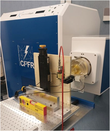
Figure 1. SIT ElectronFlash (EF) accelerator of the Centro Pisano Multidisciplinare sulla Ricerca e Implementazione Clinica della Flash Radiotherapy (CPFR) in Pisa, Italy. The experimental setup positioned on the table is shown.
The use of silicon sensors of small sensitive thickness reduces the generation of charge carriers in the active volume and the charge collection time, thus limiting the recombination and saturation effects. In addition, by etching the support wafer, sensor with a total thickness smaller than 100 microns can be obtained which would reduce the beam perturbation as required for an ideal beam monitor device. The samples chosen for the experiment are PiN silicon sensors, manufactured within the FBK [25] EXFLU1 production batch [26, 27]. Two silicon square devices (4.5 mm side length) were selected from two wafers featuring different active thickness (30 μm and 45 µm) and a total thickness of 655 and 570 μm, respectively. Each device hosts six different pad sensors of different active areas, and three of them from both wafers were tested, featuring areas of 2, 1, and 0.25 mm2 (Figure 2). The active thickness is epitaxially grown (Epi) over a thick low-resistivity handling wafer. The sensors were preliminary characterized in our department lab to verify their electrical properties. Through the analysis of the I-V curves, it was verified that they fully deplete at 10 V and the breakdown voltage occurs over 300 V of reverse bias. The sensors were mounted with conductive glue on high-voltage distribution boards, shown in Figure 2, allowing simultaneous reading of the three chosen pads connected to the output channels through wire-bonding. The guard ring of each pad was grounded.
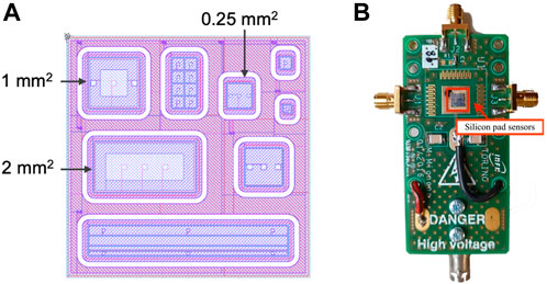
Figure 2. (A) Technical drawing of the sensors used in the experiment. Among the different implanted pads, the arrows point out the ones tested (0.25, 1, and 2 mm2). (B) The sensor mounted on the HV distribution board is represented.
The readout system used is based on the TERA08 integrated circuit, designed for medical applications by the INFN group of Torino [28]. Initially developed as a front-end electronic readout for gas monitor chambers, TERA08 performs a conversion from the instantaneous current to a digital pulse frequency, where each digital pulse corresponds to a fixed input charge quantum. It implements 64 identical channels, each featuring a converter followed by a 32 bit counter. The maximum conversion frequency is 20 MHz and the charge quantum can be selected in a range extending up to 1.115 pC [29]. For all measurements presented in this work, the value of the charge quantum was measured to be (211 ± 1) fC, in accordance with the chosen nominal setting of 200 fC. The counters were read out using a NI FlexRIO FPGA module at a frequency of 100 Hz. A data acquisition program, developed using LabView, allowed to display online the count rates of each channel and to store the data for the offline analysis.
The silicon device was aligned along the beamline, at the exit of the EF applicator, at the center of the beam spot and it was mounted on a fixed motor system positioned on a table in the EF room (Figure 3). This configuration allowed moving the silicon sensors and the FD, used to provide the reference dose measurements, in and out of the beam in the same experimental conditions. All the measurements were performed at the maximum of the depth-dose distribution in water for the 9 MeV electron beam, obtained by placing a 12 mm thick solid water slab sandwiched between the applicator and the detector holder. Both silicon sensors and FD were enclosed in 3D-printed PLA boxes with an opening window in front of the active sensor surface to ensure the same air-gap distance (7 mm) between the sensors and the 12 mm thick solid water slab. For twelve values of the beam current at the exit window in the available range (1–100 mA), several EF parameters, such as magnetron power and bias of the cathode, have been optimized in order to have a constant energy spectrum. These twelve “working points” have been named according to the dose values measured in water at the build-up depth, using the 10 cm diameter applicator during the commissioning procedure. The “working points” labels (WPlabels) need to be converted into the actual dose related to the specific irradiation point and applicator considered. Table 1 reports the correspondence between the nine (out of the twelve possible) WPlabels considered in the test and the corresponding values measured by the FD for the 30 mm diameter applicator. The reference setup for measurements with the FD relies in positioning it in a cylindrical PMMA phantom of 120 mm diameter (ref setup), while in the experimental setup considered in this test the FD was positioned in the already described 3D-printed PLA box (test setup). Therefore, in order to obtain the values of effective dose-in-water, the discrepancy in the response of the FD in the ref or test setup was studied by means of Geant4 Monte Carlo simulations. More specifically, the Monte Carlo simulations included the support structure of the sensor, the 3D-printed PLA box and the 12 mm thick build-up slab for the test setup, the PMMA cylindrical water equivalent holder and the build-up slab for the ref setup. All the components were positioned at the applicator exit. In both cases, simulations were based on the “eFLASH radiotherapy” example code, available in Geant4 11.0, which includes the EF accelerator and different applicator geometries. The energy spectrum of the primary electrons was measured, showing a slight decrease in the beam’s mean energy due to the low-energy tail presence. The lateral scattering contribution due to the presence of the FD holder was quantified. The Geant4 simulations were run with “G4EmStandardPhysics_option4,” “G4RadioactiveDecayPhysics,” and “G4DecayPhysics” physics list, while cut-offs for all particle productions were set to 0.01 mm. The electron dose was scored along a 1.9 × 1.9 × 10 cm3 water volume in a grid with 1.9 × 1.9 × 1 mm3 resolution, with and without a 10 × 10 × 10 cm3 water phantom all around to simulate the contribution of the cylindrical PMMA phantom. The simulations were performed with 108 particles. In these conditions, a 3.9% increase in the deposited dose was found when considering the cylindrical PMMA phantom. The values reported in the following table were corrected for this effect. A maximum dose-per-pulse of 10.2 ± 0.3 Gy was reached.
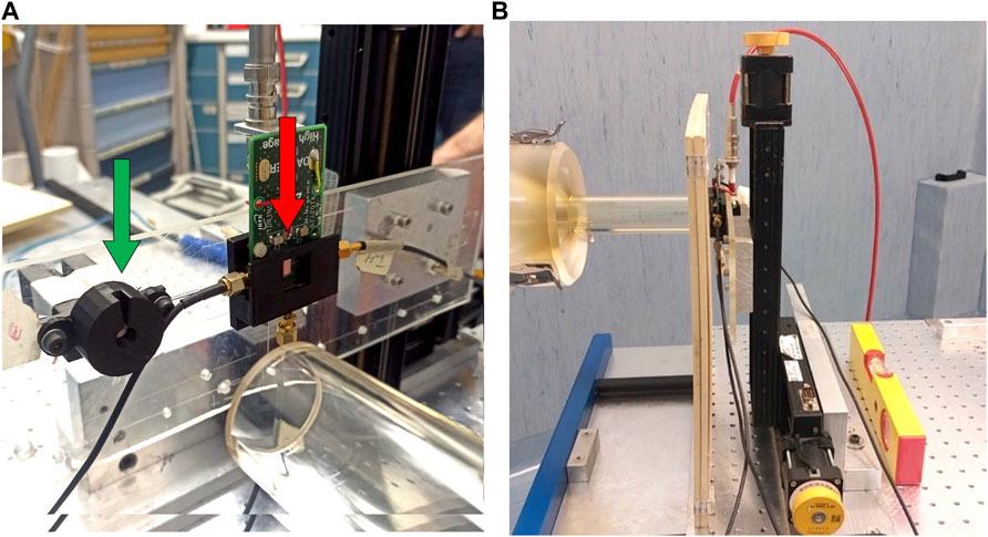
Figure 3. (A) The silicon sensor (right arrow) and the FlashDiamond (left arrow) mounted on the same supporting structure. The two 3D printed boxes (in black) in which the sensors are positioned are visible. (B) The EF applicator, in contact with the solid water slab, adjacent to the sensor support box is shown.
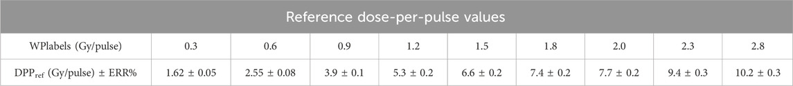
Table 1. Reference dose-per-pulse (DPP) values measured by the FlashDiamond at nine increasing beam current values, identified by the corresponding nine “working points” labels (WPlables), for the irradiation point and the EF applicator considered in the test experimental setup. One measurement was performed for each WPlabel. The values measured with the FlashDiamond are reported with the corresponding error (± 3%).
For part of the test, a sensor pad of 2 mm2 active area from the device of 45 µm thickness was connected to the TERA08 chip. Since the latter can read a maximum current of 4 µA per channel before saturation, the sensor signal was split into 64 channels. As reported in a previous publication [29], such an arrangement allows to extend the current range up of 256 µA preserving a linearity better than 1% in the whole range. A specific fan-in board was used to allow the splitting of the input into the TERA08 channels. Moreover, in order to cope with the large instantaneous input current during each pulse, an RC circuit was added between the sensor output and the TERA08 input such that the charge produced by each pulse is stored in the capacitor, which discharges into the TERA08 input with a time constant much larger than the pulse duration. A series resistance value of 156 kΩ and a capacitance value of 470 nF, connected to the reference voltage of the TERA08 input, were used. Figure 4A shows a typical signal consisting of 10 pulses at a frequency of 5 Hz after software acquisition. In Figure 4B, the value of the time constant τ, determined by fitting an exponential curve to a single-pulse discharge data, is reported and is found to be in good agreement with the product RC.
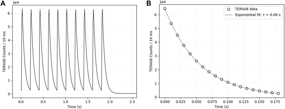
Figure 4. Example of acquisition with the TERA08 chip. (A) TERA08 counts as a function of acquisition time for an entire run, where 10 pulses with a frequency of 5 Hz are clearly distinguishable. (B) Zoom on a single signal of the discharge of the capacitor. The exponential fit results for the τ value is reported in the figure legend.
A second part of the beam time was dedicated to the test of three sensor pads of active areas 2, 1 and 0.25 mm2 from the 45 µm active thickness wafer connected directly to three input channels of an oscilloscope (Keysight Infiniium S-series DSOS254, 20 G/s sampling rate), with input impedance of 50 Ω. Through the oscilloscope, it was possible to visualize and store the voltage signal generated from the pulses delivered by the EF and its temporal structure. An example of an acquisition with the oscilloscope of one single pulse of 4 µs duration is shown in Figure 5, where three waveforms corresponding to each output channel are represented with three different colors. The shapes of the signals, characterized by an initial spike followed by an increase up to a broad maximum at the center of the pulse, were found to be perfectly compatible with those recorded by the machine’s internal BCTs. The total charge of each pulse was obtained by dividing the integral of the acquired waveforms by the input impedance of the oscilloscope.
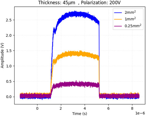
Figure 5. Waveforms acquired by the oscilloscope for a 4 μs pulse delivered by the EF at 3.89 Gy/pulse dose-per-pulse. Three sensors of different active areas (2, 1, and 0.25 mm2) were connected to 3 channels of the oscilloscope, represented in different colors in the plot. The data correspond to the 45 µm thick sensor inversely biased at 200 V.
The charge per pulse measurements acquired with a silicon pad of 2 mm2 area and 45 µm active thickness, using both TERA08 and the oscilloscope, are shown in Figure 6 as a function of the dose-per-pulse up to ∼10 Gy/pulse. The sensor was reverse-biased at 200 V, well above his depletion voltage, to ensure operating the sensor under saturated drift velocity of charge carriers. Each point represents the average charge of the ten pulses used for the measurement. The charges measured with TERA08 and using the oscilloscope are found to be compatible within the uncertainties. Both data sets show very good linearity, resulting in a coefficient of determination of a linear fit R2 > 0.99.
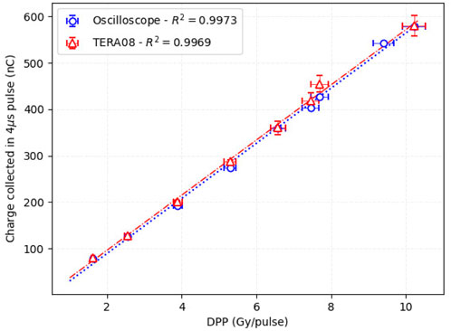
Figure 6. The charge produced in one pulse of 4 μs duration as a function of the dose-per-pulse is represented for both TERA08 and oscilloscope data. A coefficient of determination R2 > 0.99 was obtained in both cases. The data correspond to the pad of 2 mm2 area and 45 µm active thickness, inversely polarized at 200 V.
Figure 7 shows the charge collected in the six different pads considered (2, 1, and 0.25 mm2 active areas for both 45 and 30 µm thicknesses), where the bias voltage in the case of the thinner device was set to 133.34 V to achieve the same internal electric field (∼4.44 V/μm) and thus saturation of the charge carriers drift velocity. For all the pads, the collected charge showed a very linear behavior as a function of the dose-per-pulse. At the same dose per pulse, the collected charge varies proportionally to the pad area and to the sensor thickness. In addition, the ratio between charges collected in different pads is found to be independent of the dose-per-pulse, indicating that volume-dependent effects of recombination of charge carriers are playing a negligible effect.
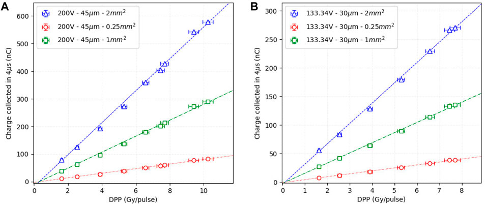
Figure 7. The results of the charge collected in each pulse for the 3 sensor pads of the 45 µm device are shown in (A), while the ones of the 30 µm macro-sensor in (B). In order to have the same electric field condition within the active thickness, the first sensor was inversely polarized at 200 V, while the second one at 133.34 V.
The energy deposited in the active layer of silicon sensors of different geometries and the corresponding total charge produced was simulated with Allpix Squared framework (v 2.4.0) [30]. The electron source was defined with a radius of 2 mm and the energy spectrum was set as the one obtained at the applicator exit from the “eFLASH radiotherapy” Geant4 example. The deposited charges have been assumed to be equal to the propagated charges at the readout electronics.
For both sensor thicknesses 107 events have been simulated. Assuming a linear increase of the charge with the number of initial particles, the collection of charge can be estimated for a larger number of initial particles. In the case of 30 μm thick sensors, the simulation results are compatible with all those obtained experimentally within 2.0% for the 2 mm2 area, 6.2% for the 1 mm2 one, and 4.1% for the 0.25 mm2 one. In the case of 45 μm thick sensors, the simulation results are compatible with the experimental ones within 8.1% for the 2 mm2 area, 13.5% for the 1 mm2 area, and 17.6% for the 0.25 mm2 area. Although the grounded guard ring, a slight broadening of the depletion region into the silicon could explain the higher value of the charge collected in respect to the simulated one, and this has a larger impact in the 45 μm case. Further studies are ongoing to investigate and verify this effect.
As previously reported, data acquired at 200 V bias voltage show perfect linearity for the whole range of dose-per-pulse values investigated. However, by decreasing the bias voltage, a saturation effect of the charge collected was observed from values of dose-per-pulse >3.89 Gy/pulse. This effect is illustrated in Figure 8 which shows the charge collected in a 4 µs pulse in a 2 mm2 area pad, 45 µm thick, as a function of the dose-per-pulse for different polarization voltages.
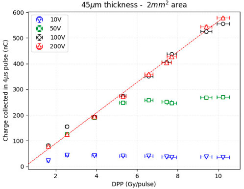
Figure 8. Charge produced in 4 μs pulses as a function of the dose in each pulse in a 2 mm2 area and 45 µm active thickness pad inversely polarized at 10, 50, 100, and 200 V. The data were acquired with the oscilloscope.
To further investigate the effect, Figure 9A shows the waveforms of a pulse as a function of the dose-per-pulse for 200 V polarization, as acquired with the oscilloscope. As expected, the signal amplitude increases as the dose-per-pulse increases, while keeping the pulse duration constant (4 µs). A peak is present at the beginning of the pulse, which is more evident at higher dose-per-pulse, and was also present in the BCT signal, thus not relying on the internal effects of the sensor. On the other hand, the waveforms for the measurements taken at 50 V (Figure 9B) show a distortion of the signal shape for dose-per-pulse values >3.89 Gy/pulse. The signal duration is shorter than 4 µs, and the integrated value reaches a constant value. The detector continues to be irradiated but the e/h pairs created are no longer collected. The hypothesis that the high density of charge carriers generates an opposing electric field that cancels the drift field, inhibiting charge collection, is currently under study by models and simulations.
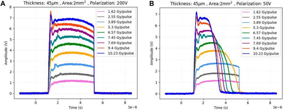
Figure 9. Waveforms acquired with the oscilloscope for pulses at nine different dose-per-pulse conditions. The data correspond to the pad with 2 mm2 area and 45 µm active thickness, inversely polarized at 200 V (A) and 50 V (B).
The UHDR scenario poses challenges, mainly related to ion recombination effects, for radiation detectors dedicated to both real-time beam monitoring and reference dosimetry. However, beam monitors are characterized by supplementary specifications with respect to dosimeters, which are more demanding when dealing with FLASH beams: high spatial and temporal resolution to measure the beam profile and provide a feedback/interlock signal to the acceleration system, beam transparency, large response dynamic range, large sensitive area to enclose the entire beam cross-section and radiation hardness.
In this study, the results of the test of different silicon sensor geometries exposed to 9 MeV electron beams from the EF machine of the CPFR (Pisa, Italy) were presented. The main advantages of using silicon sensors as beam monitoring devices lie in the possibility of a) polarizing them up to very high voltages, larger than 300 V, to overcome the problem of charge saturation and signal distortion, b) reducing the active area and thickness to lower the amount of charge produced in the device and to increase the beam transparency and c) exploiting the excellent spatial resolution. The latter does not represent a priority when a low energy dedicated FLASH LINAC, like the Pisa EF, is considered, since BCTs are perfectly suited to provide current measurements, while beam uniformity and flatness measurements are performed moving a point-like dosimeter (e.g., FD) in the irradiation field. However, even in this experimental setup, a silicon sensor able to cover the entire diameter of the EF applicator exit could provide a measure of the beam profile in a unique beam shot, reducing the number of spots needed to scan the field with a point-like detector and thus cutting down the delivered dose. In addition, the availability of detectors with excellent spatial resolution gains attention in the realm of Very High Electron Energy (VHEE) research. Recently, the idea of investigating the use of VHEE beams (50–200 MeV) aims at investigating and exploiting the FLASH effect of electrons at penetration depths larger than the superficial ones reached by low energy beams. Small diameter VHEE beams can be scanned in a pencil-beam-like modality and focused, producing finer resolution for intensity modulated treatments than photon beams, and accelerators may be constructed at significantly lower cost compared to the current installations required for protons beams [17, 18].
Silicon pads of 30/655 µm or 45/570 µm active/total thickness and areas 2, 1, 0.25 mm2 were investigated as potential solutions for monitoring UHDR beams. Future tests will be performed with thinner active thicknesses (10 and 20 μm, also available within the same batch) and with thinned down sensors (100 or 120 µm total thickness) to verify beam transparency. The charge collected by the sensors during irradiation was measured with an oscilloscope and the TERA08 chip. Several measurements were made up to very high dose rates of 2.5·106 Gy/s, corresponding to ∼10 Gy in pulses of 4 μs duration and a good linearity (R2 > 0.99) was verified for both readout systems, as well as a very good compatibility of the two measurements. This work aimed at studying the response linearity of silicon sensors as a first step towards their possible application in UHDR electron beams. However, it also allowed verifying that no sign of signal degradation, e.g., depletion voltage or leakage current increase [31], appeared after a total cumulative dose of more than 9 kGy. The cumulative dose a beam monitor needs to withstand to comply with the UHDR requirements is still difficult to be estimated, but the radiation hardness is obviously a critical characteristic for solid-state sensors in this realm. Although the larger bandgap and e-h pair production energy of SiC and diamond compared to silicon make them more suitable for applications in UHDR beams [14, 32], it is interesting to evaluate the limits in terms of radiation hardness of silicon sensors, which could benefit of a greater technological maturity in respect to SiC and diamonds.
Simulation tools (Geant4 Monte Carlo and Allpix Squared) were implemented, and the simulation results were in good agreement with the experimental data, opening the possibility to simulate the performance of different silicon geometries and experimental setups configurations. Further studies and simulations with Sentaurus TCAD are ongoing to better understand the distortion of the signal occurring at lower bias voltages.
The results obtained by splitting the sensor output in all 64 chip channels of the TERA08 chip open the way to the chip adaptation towards the readout of multiple silicon pads/strips, aiming at enlarging the sensitive area of the beam monitoring device. Taking into account the maximum current that a single channel of the TERA08 can sustain (4 µA), the total number of chip channels (64), and the charge measured by the chip under high dose rate conditions (about 600 nC at the maximum 10.2 Gy/pulse dose rate value), more than one chip can be considered to measure the charge collected in an hypothetical multiple strip/pad silicon sensor. Keeping constant the signal readout circuit (R ≃ 156 kΩ and C ≃ 470 nF) and the silicon pad characteristics (2 mm2, 45 µm thickness) used in the described test and by computing the maximum of the function describing the number of counts read by TERA08 chip (N(t) = Ntot (1—exp (t/τ))), splitting the sensor output in only 3 TERA08 channels (instead of the all 64 channels, as done in the test) would be sufficient to avoid reaching electronic saturation. This would then allow to simultaneously readout ∼20 sensors with the same chip. These estimations would improve with the use of sensors thinner than those presented in this work and with the use of an upgraded version of TERA08 with a higher current range (TERA09, 12 µA of maximum instantaneous current per channel using a charge quantum of 200 fC).
In conclusion, this preliminary work demonstrates the response linearity of thin silicon sensors’ prototypes in UHDR electron beam irradiation. Further studies will be performed to test the sensors radiation hardness, to enlarge the sensitive area of the detector, to develop the proper readout electronics, to test adapted prototypes to other beam types, such as UHDR proton beams.
The raw data supporting the conclusions of this article will be made available by the authors, without undue reservation.
EM: Conceptualization, Data curation, Formal Analysis, Investigation, Methodology, Software, Visualization, Writing–original draft, Writing–review and editing. AF: Conceptualization, Data curation, Formal Analysis, Investigation, Methodology, Software, Visualization, Writing–original draft, Writing–review and editing. MA: Investigation, Validation, Writing–review and editing. AC: Conceptualization, Data curation, Formal Analysis, Investigation, Methodology, Software, Writing–original draft. MC: Investigation, Methodology, Resources, Supervision, Validation, Writing–review and editing. ED: Investigation, Validation, Writing–review and editing. DD: Investigation, Methodology, Resources, Supervision, Validation, Writing–review and editing. UD: Conceptualization, Data curation, Formal Analysis, Investigation, Methodology, Software, Writing–original draft. FD: Investigation, Methodology, Resources, Supervision, Validation, Writing–review and editing. MFM: Investigation, Validation, Writing–review and editing. MF: Investigation, Methodology, Resources, Supervision, Validation, Writing–review and editing. VF: Investigation, Validation, Writing–review and editing. SG: Conceptualization, Funding acquisition, Investigation, Methodology, Project administration, Supervision, Validation, Writing–review and editing. OM: Conceptualization, Data curation, Formal Analysis, Investigation, Methodology, Software, Writing–original draft. MAH: Investigation, Validation, Writing–review and editing. FM: Conceptualization, Funding acquisition, Investigation, Methodology, Project administration, Supervision, Validation, Writing–review and editing. LM: Investigation, Methodology, Resources, Supervision, Validation, Writing–review and editing. DM: Conceptualization, Data curation, Formal Analysis, Investigation, Methodology, Software, Writing–original draft. MM: Investigation, Methodology, Resources, Supervision, Validation, Writing–review and editing. GP: Investigation, Methodology, Resources, Supervision, Validation, Writing–review and editing. JP: Investigation, Methodology, Resources, Supervision, Validation, Writing–review and editing. VS: Investigation, Methodology, Resources, Supervision, Validation, Writing–review and editing. RC: Conceptualization, Funding acquisition, Investigation, Methodology, Project administration, Supervision, Validation, Writing–review and editing. RS: Conceptualization, Funding acquisition, Investigation, Methodology, Project administration, Supervision, Validation, Writing–review and editing. AV: Conceptualization, Funding acquisition, Investigation, Methodology, Project administration, Supervision, Validation, Writing–review and editing.
The author(s) declare that financial support was received for the research, authorship, and/or publication of this article. This research was supported by INFN CSN5 funded project “FRIDA” and by the VIGA_S1921_EX-POST_21_01 (Compagnia di San Paolo). Part of the EXFLU1 batch has been funded by the European Union’s Horizon 2020 Research and Innovation programme under Grant Agreement No 101004761.
We thank INFN CSN5 funded project “eXFlu” for the collaboration and “Fondazione Pisa” for funding CPFR with the grant “prog. n. 134/2021".
The authors declare that the research was conducted in the absence of any commercial or financial relationships that could be construed as a potential conflict of interest.
All claims expressed in this article are solely those of the authors and do not necessarily represent those of their affiliated organizations, or those of the publisher, the editors and the reviewers. Any product that may be evaluated in this article, or claim that may be made by its manufacturer, is not guaranteed or endorsed by the publisher.
1. Farr J, Grilj V, Malka V, Sudharsan S, Schippers M. Ultra-high dose rate radiation production and delivery systems intended for FLASH. Med Phys (2022) 49(7):4875–911. doi:10.1002/MP.15659
2. Romano F, Bailat C, Jorge PG, Lerch MLF, Darafsheh A. Ultra-high dose rate dosimetry: challenges and opportunities for FLASH radiation therapy. Med Phys (2022) 49(7):4912–32. doi:10.1002/MP.15649
3. Gómez F, Gonzalez-Castaño DM, Fernández NG, Pardo-Montero J, Schüller A, Gasparini A, et al. Development of an ultra-thin parallel plate ionization chamber for dosimetry in FLASH radiotherapy. Med Phys (2022) 49(7):4705–14. doi:10.1002/MP.15668
4. Zou W, Diffenderfer ES, Ota K, Boisseau P, Kim MM, Cai Y, et al. Characterization of a high-resolution 2D transmission ion chamber for independent validation of proton pencil beam scanning of conventional and FLASH dose delivery. Med Phys (2021) 48(7):3948–57. doi:10.1002/MP.14882
5. Tinganelli W, Sokol O, Quartieri M, Puspitasari A, Dokic I, Abdollahi A, et al. Ultra-high dose rate (FLASH) carbon ion irradiation: dosimetry and first cell experiments. Int J Radiat Oncol Biol Phys (2022) 112(4):1012–22. doi:10.1016/J.IJROBP.2021.11.020
6. Di Martino F, Del Sarto D, Giuseppina Bisogni M, Capaccioli S, Galante F, Gasperini A, et al. A new solution for UHDP and UHDR (Flash) measurements: theory and conceptual design of ALLS chamber. Physica Med (2022) 102:9–18. doi:10.1016/J.EJMP.2022.08.010
7. Giordanengo S, Guarachi LF, Braccini S, Cirrone GAP, Donetti M, Fausti F, et al. Fluence beam monitor for high-intensity particle beams based on a multi-gap ionization chamber and a method for ion recombination correction. Appl Sci (2022) 12(23):12160. doi:10.3390/APP122312160
8. Gonçalves Jorge P, Grilj V, Bourhis J, Vozenin MC, Germond JF, Bochud F, et al. Technical note: validation of an ultrahigh dose rate pulsed electron beam monitoring system using a current transformer for FLASH preclinical studies. Med Phys (2022) 49(3):1831–8. doi:10.1002/MP.15474
9. Liu K, Palmiero A, Chopra N, Velasquez B, Li Z, Beddar S, et al. Dual beam-current transformer design for monitoring and reporting of electron ultra-high dose rate (FLASH) beam parameters. J Appl Clin Med Phys (2023) 24(2):e13891. doi:10.1002/ACM2.13891
10. Oesterle R, Gonçalves Jorge P, Grilj V, Bourhis J, Vozenin MC, Germond JF, et al. Implementation and validation of a beam-current transformer on a medical pulsed electron beam LINAC for FLASH-RT beam monitoring. J Appl Clin Med Phys (2021) 22(11):165–71. doi:10.1002/ACM2.13433
11. Ashraf MR, Rahman M, Zhang R, Williams BB, Gladstone DJ, Pogue BW, et al. Dosimetry for FLASH radiotherapy: a review of tools and the role of radioluminescence and cherenkov emission. Front Phys (2020) 8:570033. doi:10.3389/fphy.2020.00328
12. Levin DS, Ferretti C, Ristow N, Tecchio M, Friedman PS, Litzenberg DW, et al. A scintillator beam monitor for real-time FLASH radiotherapy. ArXiv (2023).
13. Trigilio A, De Gregorio A, Fischetti M, Franciosini G, Garbini M, Lippa G, et al. The FlashDC project: development of a beam monitor for FLASH radiotherapy. Nucl Instr Methods Phys Res Section A: Acc Spectrometers, Detectors Associated Equipment (2022) 1041:167334. doi:10.1016/J.NIMA.2022.167334
14. Romano F, Milluzzo G, Di Martino F, D’Oca MC, Felici G, Galante F, et al. First characterization of novel silicon carbide detectors with ultra-high dose rate electron beams for FLASH radiotherapy. Appl Sci (2023) 13(5):2986. doi:10.3390/APP13052986
15. Vignati A, Giordanengo S, Fausti F, Martì Villarreal OA, Mas Milian F, Mazza G, et al. Beam monitors for tomorrow: the challenges of electron and photon FLASH RT. Front Phys (2020) 8:375. doi:10.3389/fphy.2020.00375
16. Fausti F, Olave J, Giordanengo S, Ali OH, Mazza G, Rotondo F, et al. A single ion discriminator ASIC prototype for particle therapy applications. Nucl Instr Methods Phys Res Section A: Acc Spectrometers, Detectors Associated Equipment (2021) 985:164666. doi:10.1016/J.NIMA.2020.164666
17. Ronga MG, Cavallone M, Patriarca A, Maia Leite A, Loap P, Favaudon V, et al. Back to the future: very high-energy electrons (VHEEs) and their potential application in radiation therapy. Cancers (2021) 13(19):4942. doi:10.3390/CANCERS13194942
18. Sarti A, De Maria P, Battistoni G, De Simoni M, Di Felice C, Dong Y, et al. Deep seated tumour treatments with electrons of high energy delivered at FLASH rates: the example of prostate cancer. Front Oncol (2021) 11:777852. doi:10.3389/FONC.2021.777852
19. Marti Villarreal OA, Vignati A, Giordanengo S, Abujami M, Borghi G, Centis Vignali M, et al. Characterization of thin LGAD sensors designed for beam monitoring in proton therapy. Nucl Instr Methods Phys Res Section A: Acc Spectrometers, Detectors Associated Equipment (2023) 1046:167622. doi:10.1016/J.NIMA.2022.167622
20. Vignati A, Abujami M, Bersani D, Borghi G, Centis Vignali M, Data E, et al. Monitoring therapeutic proton beams with LGAD silicon detectors. J Instrumentation (2022) 17(11):C11001. doi:10.1088/1748-0221/17/11/C11001
21. Vignati A, Giordanengo S, Milian FM, Ganjeh ZA, Donetti M, Fausti F, et al. A new detector for the beam energy measurement in proton therapy: a feasibility study. Phys Med Biol (2020) 65(21):215030. doi:10.1088/1361-6560/ABAB58
22. SIT. S.I.T. Sordina IORT technologies S.P.A (2023). Available at: https://www.soiort.com/ (Accessed on July 12, 2023).
23. Di Martino F, Barca P, Barone S, Bortoli E, Borgheresi R, De Stefano S, et al. FLASH radiotherapy with electrons: issues related to the production, monitoring, and dosimetric characterization of the beam. Front Phys (2020) 8:570697. doi:10.3389/fphy.2020.570697
24. Marinelli M, Felici G, Galante F, Gasparini A, Giuliano L, Heinrich S, et al. Design, realization, and characterization of a novel diamond detector prototype for FLASH radiotherapy dosimetry. Med Phys (2022) 49(3):1902–10. doi:10.1002/MP.15473
25. FBK. FBK center for sensors and devices (2023). Available at: https://sd.fbk.eu/en/ (Accessed on July 12, 2023).
26. Croci T, Morozzi A, Sola V, Asenov P, Fondacci A, Giordanengo S, et al. TCAD optimization of LGAD sensors for extremely high fluence applications. J Instrumentation (2023) 18(01):C01008. doi:10.1088/1748-0221/18/01/C01008
27. Sola V, Paternoster G, Arcidiacono R, Asenov P, Borghi G, Boscardin M, et al. Advances in LGAD technology for high radiation environments (2023). doi:10.1088/1748-0221/6/06/P06013
28. La Rosa A, Mazza G, Donetti M, Marchetto F, Luetto L, Attili A, et al. Design and test of a 64-channel charge measurement ASIC developed in CMOS 0.35 μm technology. Nucl Instr Methods Phys Res Section A: Acc Spectrometers, Detectors Associated Equipment (2007) 583(2–3):461–8. doi:10.1016/J.NIMA.2007.09.024
29. Cirio R, Fausti F, Fanola Guarachi L, Giordanengo S, Marchetto F, Mazza G, et al. A simple method to increase the current range of the TERA chip in charged particle therapy applications. Nucl Instr Methods Phys Res Section A: Acc Spectrometers, Detectors Associated Equipment (2015) 798:107–10. doi:10.1016/J.NIMA.2015.07.013
30. Allpix Squared. Semiconductor detector Monte Carlo simulation framework (2023). Available at: https://allpix-squared.docs.cern.ch/ (Accessed on July 12, 2023).
31. Radu R, Fretwurst E, Klanner R, Lindstroem G, Pintilie I. Radiation damage in n-type silicon diodes after electron irradiation with energies between 1.5 MeV and 15 MeV. Nucl Instr Methods Phys Res Section A: Acc Spectrometers, Detectors Associated Equipment (2013) 730:84–90. doi:10.1016/j.nima.2013.04.080
Keywords: FLASH radiotherapy, ultra-high dose rate electron beams, beam monitoring, silicon sensors, TERA chip
Citation: Medina E, Ferro A, Abujami M, Camperi A, Centis Vignali M, Data E, Del Sarto D, Deut U, Di Martino F, Fadavi Mazinani M, Ferrero M, Ferrero V, Giordanengo S, Martì Villarreal OA, Hosseini MA, Mas Milian F, Masturzo L, Montalvan Olivares DM, Montefiori M, Paternoster G, Pensavalle JH, Sola V, Cirio R, Sacchi R and Vignati A (2024) First experimental validation of silicon-based sensors for monitoring ultra-high dose rate electron beams. Front. Phys. 12:1258832. doi: 10.3389/fphy.2024.1258832
Received: 14 July 2023; Accepted: 02 February 2024;
Published: 26 February 2024.
Edited by:
Marco Borghesi, Queen’s University Belfast, United KingdomReviewed by:
Pedro M. M. Correia, University of Aveiro, PortugalCopyright © 2024 Medina, Ferro, Abujami, Camperi, Centis Vignali, Data, Del Sarto, Deut, Di Martino, Fadavi Mazinani, Ferrero, Ferrero, Giordanengo, Martì Villarreal, Hosseini, Mas Milian, Masturzo, Montalvan Olivares, Montefiori, Paternoster, Pensavalle, Sola, Cirio, Sacchi and Vignati. This is an open-access article distributed under the terms of the Creative Commons Attribution License (CC BY). The use, distribution or reproduction in other forums is permitted, provided the original author(s) and the copyright owner(s) are credited and that the original publication in this journal is cited, in accordance with accepted academic practice. No use, distribution or reproduction is permitted which does not comply with these terms.
*Correspondence: Arianna Ferro, YXJpYW5uYS5mZXJybzc2N0BlZHUudW5pdG8uaXQ=
†These authors have contributed equally to this work and share first authorship
‡These authors share last authorship
Disclaimer: All claims expressed in this article are solely those of the authors and do not necessarily represent those of their affiliated organizations, or those of the publisher, the editors and the reviewers. Any product that may be evaluated in this article or claim that may be made by its manufacturer is not guaranteed or endorsed by the publisher.
Research integrity at Frontiers
Learn more about the work of our research integrity team to safeguard the quality of each article we publish.