
95% of researchers rate our articles as excellent or good
Learn more about the work of our research integrity team to safeguard the quality of each article we publish.
Find out more
ORIGINAL RESEARCH article
Front. Phys. , 03 January 2024
Sec. Radiation Detectors and Imaging
Volume 11 - 2023 | https://doi.org/10.3389/fphy.2023.1321541
This article is part of the Research Topic Pushing Frontiers - Imaging For Photon Science View all 19 articles
 Heinz Graafsma1,2,3*†
 Jonathan Correa1,2†Sergei Fridman1,2†Helmut Hirsemann1,2†S. M. A. Hosseini-Saber1,2†Alexandr Ignatenko4†
 Alexander Klujev1,2†Sabine Lange1,2†
 Torsten Laurus1,2†
 Alessandro Marras1,2†
 David Pennicard1,2†Seungyu Rah1,2†Sandra Schneider1†Ofir Shefer Shalev1†Thorsten Stoye1†Ulrich Trunk1,2†
 Cornelia B. Wunderer1,2†
The past, current and planned future developments of X-ray imagers in the Photon-Science Detector Group at DESY-Hamburg is presented. the X-ray imagers are custom developed and tailored to the different X-ray sources in Hamburg, including the storage ring PETRA III/IV; the VUV-soft X-ray free electron laser FLASH, and the European Free-Electron Laser. Each source puts different requirements on the X-ray detectors, which is described in detail, together with the technical solutions implemented.
The continuous exponential improvement in X-ray sources at synchrotron storage rings [1, 2] and Free-Electron Lasers [3] means that significant improvements in X-ray imagers are needed in order to maximize the scientific output, both in quality and quantity. Keeping up with the increase in source brilliance by an order of magnitude every 3 years, is, however, a major challenge. To put this into perspective, to develop a new detector from idea to installation at the experimental station takes roughly 10 years when the concept is new. This means that the source brilliance increases by 3 orders of magnitude during the development time of the detector. In addition, the large variety of experimental techniques, especially at storage rings [2], results in very diverse, and often conflicting detector requirements, so that different detector systems need to be developed.
In Hamburg the situation is even more challenging due to very different photon sources. PETRA III is a 6 GeV storage ring catering mainly to the medium to high photon energy synchrotron community. This is very different to the FLASH facility, which is a 1.35 GeV Free-Electron Laser using super conducting accelerator technology. It produces photons in the VUV to soft X-ray regime in a burst mode operation. It produces pulse trains up to 800 micro-seconds long, with a train repetition frequency of 10 Hz and up to 500 pulses in each train. The European X-ray Free-Electron Laser uses the same superconducting accelerator technology as FLASH, but runs at 17 GeV and produces photons in the soft, medium and hard X-ray regime. The pulse trains are 600 micro-seconds long, are repeated with a 10 Hz frequency, and can contain up to 2,700 pulses.
There are many fundamental differences between a storage ring and a Free-Electron Laser, both from an experimental and a detector point of view. Storage rings can often be regarded as continuous sources and data is mostly collected with many consecutive pulses. Free-Electron Lasers on the other hand are mostly used as pulsed sources, where an image is recorded for every single pulse. This is both useful, since single FEL pulses are often strong enough to produce a statistically significant image, and also required, since a single pulse often destroys the sample. This has many consequences for the detectors at Free-Electron Lasers. First, the photon-counting technique, widely applied at storage rings, cannot be used, since all photons arrive at the same time, and charge integrating front-ends are required instead. At storage rings, the desired dynamic range can be obtained by either extended exposure times, or multiple exposures. At Free-Electron Lasers, a single shot image has to be able to cover the entire dynamic range. For Free-Electron Lasers based on superconducting accelerators, frame rates of up to 4.5 MHz, corresponding to the pulse rate of the source, are additionally required. Even though the time structure of the European XFEL and FLASH are comparable, their photon energies are so different that conceptually different detectors are required.
In the following section we will present the detector systems that we have developed specifically for the European XFEL and FLASH, including ongoing improvements and additional systems under construction. Based on these developments and other previous projects, we are developing two new systems, CoRDIA and TEMPUS, which are tailored for the upgraded source PETRA-IV. The developments and current status will be presented in the subsequent section. In the final section we will discuss the future directions of our developments.
With the construction of the European X-ray Free-Electron Laser, conceptually new X-ray imagers were required [4]. A few of the most challenging requirements were that in a single shot the entire dynamic range from single photons to more than 104 photons per pixel had to be covered, with a frame rate of 4.5 MHz. Additionally, as many frames as possible needed to be recorded during the 600 micro-second long pulse trains. Following a call for proposals three projects were selected; The Large Pixel Detector (LPD) [5], the DePMOS Sensor with Signal Compression (DSSC) [6], and the Adaptive Gain Integrating Pixel Detector, AGIPD [7]. Each system tackled the challenges with a different concept and targeted different applications [4]. Here only the AGIPD system, developed under the leadership of the DESY photon science detector group, will be described. The LPD system was developed by the Rutherford-Appleton Laboratory in the United Kingdom. The DSSC system was developed by a larger consortium, initially under the leadership of the Max-Planck Semiconductor Laboratory in Munich, and later under the leadership of the European XFEL itself.
The AGIPD system was developed by a consortium of DESY, PSI, University of Hamburg and University of Bonn. The AGIPD ASIC employs a charge integrating frontend with adaptive gain, where every pixel automatically and autonomously adapts its gain to the number of incoming photons [7]. Every pixel starts in high gain mode, with a small feedback capacitor, allowing for single photons to be distinguished from the noise. As soon as the voltage over the feedback capacitor reaches a preset threshold, a second, larger, feedback capacitor is added reducing the gain and extending the dynamic range. For very strong signals a third, even larger, feedback capacitor is added, resulting in a low gain and corresponding dynamic range of 104 photons of 12 keV. At the end of the integration time the final voltage over the feedback capacitors is stored in an analog memory, together with the information of the final gain setting, i.e., which feedback capacitors were used. In this manner the required dynamic range is achieved. In pixel frame storage allows for frame rates up to 4.5 MHz, compatible with the highest pulse rate of the European XFEL. During the 99.4 millisecond interval between pulse trains, the analogue memory is read out and digitized by external ADCs and the digital information is transmitted over 10G links to the DAQ system. The pixel concept is given in Figure 1. The main parameters of the AGIPD readout ASIC are given in Table 1.
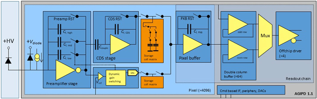
FIGURE 1. Pixel concept of the AGIPD detector.
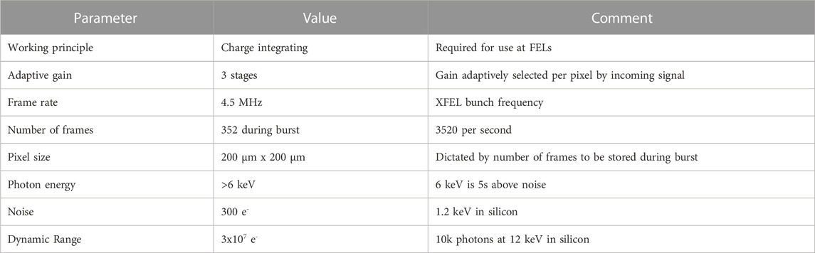
TABLE 1. Main parameters of the AGIPD readout ASIC.
An additional complication for building the system was the requirement of maximum flexibility. Two 1-million-pixel systems operate in a moderate vacuum of ≈10−6 mbar and consist of four individually movable quadrants that protrude into the sample chamber. Figure 2 shows a picture of the systems in operation at the MID and SPB/SFX instruments of the European XFEL.
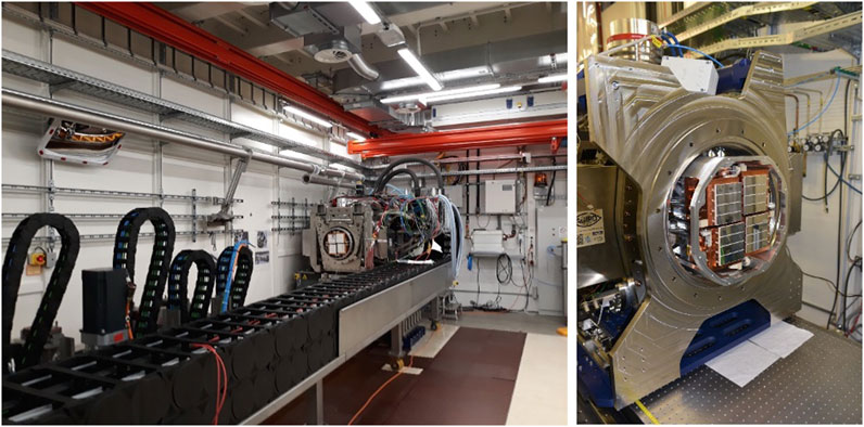
FIGURE 2. Picture of the 1-million-pixel AGIPD detector system in operation at the MID (left) and SPB/SFX (right) beamlines at the European XFEL.
The 1M-AGIPD systems have been in user operation at the SPB/SFX and MID stations since 2017 and 2019 respectively, and together produced the vast majority of the scientific user publications of the European XFEL.
Since commissioning, various improvements have been made to the system [8].
One improvement concerned the so-called late gain-switching. Wrong signal values occur when a pixel changes its gain too close to the end of the integration window, so that the output signal of the pre-amp is not yet settled when it is stored into the storage cell matrix. The proper solution to the problem is to block gain switching within the last 40 ns of the integration window, but this would require a significant redesign of the ASIC. Instead, two mitigation strategies were implemented. For experiments that do not require single photon sensitivity, automatic gain switching is disabled and the system is operated in fixed medium gain. For experiments that do not require the highest repetition rate of 4.5 MHz, extended integration times can be used. Studies have shown that extending the integration time reduces the occurrence of late gain switching in the transition region by at least three orders of magnitude.
Both MID and SPB/SFX systems will undergo an upgrade, where all the front-end modules will be replaced with new ones equipped with AGIPD1.2 ASICs. This new version fixes an issue of poor gain bit separation in the AGIPD1.1 ASICs, which resulted in an ambiguity whether medium or low gain was used.
We are currently constructing two more AGIPD cameras for the European XFEL. The first one is a 4 megapixel version for the Serial Femto-second Crystallography (SFX) user consortium, which will also be installed at the SPB/SFX instrument. This in-vacuum camera consists of two-halves, which can move independently, by 400 mm along the beam axis and ±15 mm perpendicular to it. The frontend modules will be equipped with AGIPD1.2 ASICs and silicon sensors. A CAD rendering of the 4M-AGIPD is given in Figure 3.
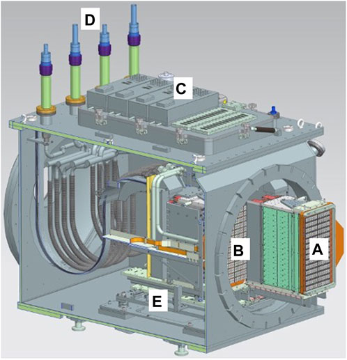
FIGURE 3. CAD rendering of the AGIPD-4M system in vacuum for the SFX user consortium at the European XFEL. (A) right half of the detector in forward position; (B) left half of detector in retracted position; (C) electrical feed-through connections for signal, power and control; (D) cooling inlets and outlets for frontend modules and readout boards; (E) translation stages.
The second system is a 1 megapixel version with high-Z sensors for the Helmholtz International Beamline for Extreme Fields (HIBEF), which will be installed at the HED instrument. High-Z sensor material is required for high photon-energies of up to 25 keV. Since the original AGIPD is hole collecting an electron collecting version of the AGIPD ASIC had to be developed [9]. The camera will initially be equipped with 500 μm silicon sensors and hole-collecting AGIPD1.2 ASICs and will later be upgraded to front-end modules with the electron collecting AGIPD1.3 ASICs and high-Z sensors. The camera is in vacuum and can be moved along the beam over 550 mm. Special care was taken for electromagnetic compatibility (EMC), required by the very high pulsed electro-magnetic fields in the experiments. A CAD rendering of the system is given in Figure 4.
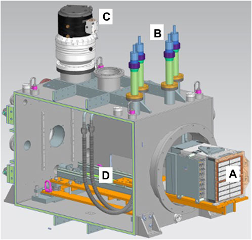
FIGURE 4. CAD rendering of the AGIPD-1M system in vacuum for the HIBEF user consortium at the European XFEL. (A) frontend modules in forward position; (B) cooling inlets and outlets for frontend and readout boards; (C) turbo pump; (D) translation stage.
To enable the long in-vacuum travel ranges along the beam axis of the two new cameras, the entire readout electronics were revised. The core idea was to combine all the functionality previously distributed over many different boards on a single readout board, which is located directly behind the frontend module in vacuum. This drastically increases modularity and improves reliability, which was compromised by the large number of connectors in the first generation systems.
A 0.5 megapixel prototype camera system based on the new readout electronics, often reffered to as mini-half, is in operation at HED instrument as part of the dDAC (dynamic Diamond Anvil Cell) compression platform [10]. Numerous user experiments have already been successfully completed with the prototype. Installation and commissioning of both new AGIPD cameras, the AGIPD-4M for the SFX user consortium and the AGIPD-1M for the HIBEF user consortium, are planned for 2024.
The Free-Electron Laser in Hamburg (FLASH) produces photons in the XUV and soft X-ray range. Developing imagers for soft X-rays is particularly hard, since in order to get the low-energy photons into the sensitive volume of the sensor, entrance windows and passivation layer thicknesses have to be kept to a minimum. As for photons below 250 eV, attenuation lengths fall significantly below 100 nm, the dead layer at the entrance should be on the order of 10 nm or less. As each photon does not create many electron-hole pairs (e.g., 69e-for 250 eV in Si), in addition care must be taken to have favorable electric fields at the surface, and the readout electronics must have low noise, preferably on the order of 10–15 electrons or less to avoid false positives in a megapixel-scale system. In order to meet the requirements for imaging experiments at FLASH, a backside-illuminated CMOS sensor, PERCIVAL, was custom designed by Rutherford Appleton Laboratory. Like AGIPD, every pixel can adapt its gain according to the incoming signal strength, using an in-pixel lateral overflow that auto-selects the capacitance used depending on the charge deposited in the pixel [11]. During pixel readout, thresholding is used to determine which capacitor(s) were needed and thus which gain was used, the corresponding voltage level is digitized on-chip, and ADC output and gain are transmitted via LVDS. The pixel concept is given in Figure 5. The main parameters of the system are given in Table 2.
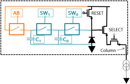
FIGURE 5. Pixel concept of the PERCIVAL sensor. The standard CMOS 3T pixel is enhanced by three switches and two capacitors. All three switches are biased at ∼0.7 V, enabling lateral overflow as the diode, then C0, then C1 reach low voltages. While SW0 and SW1 enable adding in more capacitance as needed, the third “AntiBlooming” switch provides controlled overflow for even larger charges, a preventive measure to avoid ‘blooming’ effects.
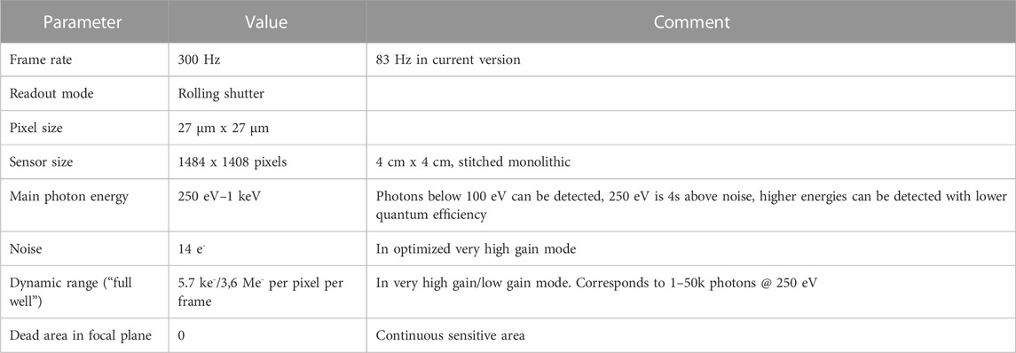
TABLE 2. Main parameters of the Percival imager.
It is the combination of these features that makes Percival an especially well-suited detector for soft X-ray scattering experiments. Detailed description of the system and its performance can be found in [11–18].
Even though the current first version of the sensor has a number of shortcomings [16] it has been used in a number of proof-of-principle user experiments, including Holography and XPCS of magnetic skyrmions at Petra III’s soft X-ray beamline P04, and single-shot Ptychography at FLASH. These exploratory experiments showed the great potential of the large dynamic range and high frame rates of Percival [18]. The shortcomings of the first version sensor–crosstalk between ADC and digital control lines, and insufficient ground connections for the pixel array that resulted in uneven biasing–are understood and are corrected in a second version of the sensor which was recently submitted to the foundry. In addition, a more compact version of the camera head has been designed; a CAD rendering is given in Figure 6.
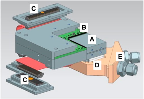
FIGURE 6. CAD rendering of the compact Percival 2M backside-illuminated CMOS camera. (A) CMOS sensor; (B) Low-Temperature Co-fired Ceramic (LTCC) interface board; (C) connectors for signals, power and control; (D) Peltier cooler (white layers); (E) water connection for Peltier cooling.
Thanks to the technological developments in accelerator technology, synchrotron storage rings world-wide are currently being upgraded [19] giving 2 or more orders of magnitude improvement in the horizontal emittance and overall source brilliance. At DESY the plan is to upgrade the accelerator PETRA III to PETRA IV, which will give an improvement of the source brilliance by a factor 500 at 10 keV and a factor of 1,000 at 60 keV photon energies [2]. This creates many new scientific possibilities, but also requires an upgrade of the current X-ray imagers. Even though an increased source brilliance does not always translate to the same increase in the number of photons to be detected, it is clear that the X-ray imagers need to have both higher flux handling capabilities (count rates), and higher frame rates. As an example, there will be enough incident photons to obtain statistically significant ptychographic images by raster scanning entire microelectronic chips with more than 100 kHz frame rates. This makes it possible, for example, to investigate a silicon chip for either defects or unwanted structures within a reasonable period of days. Another example is 3D tomography of batteries on millisecond timescales during charging and discharging, in order to follow ongoing processes at the microscopic level. All these and many more examples require X-ray imagers with a large dynamic range and frame rates of more than 100 kHz.
As described above, the European XFEL operates in a burst mode, where all X-ray pulses arrive in less than 1% of the time, the remaining 99% of the time are needed for the superconducting accelerator to cool down again. For many reasons this mode of operation is not ideal for the experiments and more evenly distributed pulses would be beneficial. Studies and developments are underway for the accelerator to stretch the pulse trains, and ultimately to distribute the pulses evenly over time, which is called continuous wave or CW operation. From a detector point of view, PETRA IV and a CW-XFEL would become more similar than PETRA III and European XFEL are at the moment. However, a 100 kHz frame rate is not sufficient for a CW-XFEL operation, where pulse frequencies of 1 MHz are expected. Since PETRA IV will almost certainly be realized before an upgrade of the European XFEL towards more CW operation, we have started the development of an imager driven by the specifications of PETRA IV. This development, CoRDIA, will be described in the next section. PETRA IV will have a large variety of experiments and techniques and not all needs will be covered by the capabilities of CoRDIA. Specifically, there will be needs for photon counting based systems, particularly in experiments with moderate X-ray flux but extremely high time resolution requirements. For these applications a system called TEMPUS is being developed, which is based on the TimePix-4 readout chip and can operate in either photon counting or time stamping modes. This system will be described in the subsequent section.
For the diffraction limited storage ring PETRA IV, a dedicated development was started at DESY building on the successful development of the AGIPD system. Some of the target specifications are given in Table 3.
TABLE 3. Target specifications for CoRDIA.
The CoRDIA (Continuous Readout Digitising Imager Array) project is a collaboration between DESY and University of Bonn. Like AGIPD, CoRDIA is a hybrid pixel detector in which read-out ASICs will be bump bonded to the semiconductor sensor. CoRDIA utilizes the same architecture for the analogue front-end in the ASIC as AGIPD, a charge-integrating pre-amplifier with adaptive gain. This allows for a dynamic range from single up to thousands of photons. To provide continuous operation without any dead time beyond the reset phase of the front-end, the readout architecture had to be developed from scratch. Compared to the systems developed for the European XFEL, frame recording is slower by a factor of ≈30, while readout frame rate needs to be faster by 2 orders of magnitude. The latter rules out analogue signal transmission due to the poor performance expected, while the input rate of ≈150 kHz conveniently allows for the digitization of multiple pixels with a single ADC. In such a scenario, memory is only needed on the level of a 2-stage S&H (sample and hold) per pixel, in order to allow simultaneous frame recording and digitization of the previous frame. As a benefit, pixel size can be shrunk considerably.
An analog stage front-end (FE) is used to collect charge generated by photons in a bump-bonded sensor. The FE circuit is compatible with electron-collecting sensors, so that a p-doped silicon sensor could be used for the main energy range (around 12 keV), while high-Z sensors could be used for harder X-ray imaging. The circuit uses the same adaptive-gain approach as AGIPD to modulate the signal amplification to the incoming photon flux. The response of the analog circuit to a charge injection, emulating photon fluxes of variable intensity (with modulation of the gain), has been tested on a test chip, at a frequency of 150k frame/s, i.e., exceeding our frame-rate requirements [20].
While a new image is stored as an analog signal in one memory circuits, the previous image stored in the other memory circuit is retrieved, processed by a correlated-double-sampling (CDS) circuit, and digitized. As soon as digital bits are produced by the ADC, they are packaged, encoded, and transmitted off-chip by a high-speed driver.
To reach a suitable trade-off between frame rate, layout size and power dissipation, a successive approximation register (SAR) ADC was designed, capable of digitizing 11 bits at 2.5 MS/s while reaching 10 ENOBs (effective number of bits net resolution). While its layout is reasonably compact, it is too large to fit within our target pixel size (110 μm × 110 µm); on the other hand, the ADC sampling speed is high enough that the signal from 16 FE circuits can sequentially be processed by the same ADC without impairing our frame rate requirements. We defined our basic structure as a 440 μm × 440 µm pixel block (“super pixel”), each including 16 analog FE circuits, a CDS and ADC circuit serving sequentially the 16 pixels, and 1/128 of the digital readout circuit.
Space has been reserved in the pixel block layout for through silicon via (TSV) landing pads that could be used for vertical integration as an alternative to traditional periphery wirebonding, so that blind silicon areas could be minimized. The inputs of the FE circuits are distributed evenly to pads on the “super pixel” surface, allowing the ASIC to be bump-bonded to a 110 µm -pixel-pitch sensor.
The readout circuit has been developed by NIKHEF, and implements the physical layer defined in the IEEE 802.3ae standard. The circuit consists of the Physical Coding Sublayer (digital) part, preparing the data for high-speed throughput (scrambling to ensure DC balance, and 64-to-66-bit encoding), and fast driver (Gigabit Wire Transmitter) able to stream out data at several GHz. The circuit has already been used in the Timepix4 ASIC (discussed later) and has been successfully tested by the Medipix4 collaboration [21] at 5.12 GHz. In our architecture, each block of 2k pixels is streamed out by one such circuits: since each pixel output is digitized with less than 16 bits, the 5.12 GHz frequency is enough to cover our frame rate requirements.
Several MPW prototypes have been designed and manufactured in TSMC 65 nm technology, see Figure 7, to validate the circuits described above as standalone blocks, up to now confirming expected performances. We acknowledge CERN and the RD53 collaboration for developing several IO blocks that were used in the design of the MPWs. A further ASIC prototype, embedding some of the blocks in a “superpixel” layout, is currently under test. We aim at developing the first version of the imager so that it will be ready for the first experiments at the PETRA-IV upgraded ring, expected in 2029.
FIGURE 7. MPW prototypes including standalone circuits for validation. From left to right: CoRDIA01 - front-end and CDS, HIS-ADC01 - SAR ADC, CoRDIA03 - multi-gigabit transmitter, CoRDA02 “superpixel” layout including front-end, CDS and ADC.
A large number of different experiments at PETRAIII have benefited from the use of one of the detectors developed at DESY, the LAMBDA detector [22]. Based on the Medipix3 photon counting readout chip [23], it has become a workhorse for many different experimental stations. The combination of a small pixel size, of 55 μm, with relatively high readout rates have made it attractive for X-ray imaging at synchrotrons. Moreover, the use of high-Z sensors (mainly CdTe and GaAs) and the option of tiling up several ASICs covering a large area, has pushed the project to a full commercialization of the detector by the DESY spin-off company X-Spectrum GmbH [24].
In that context, a new readout chip has been recently developed by the Medipix4 collaboration using 65 nm technology, Timepix4 [21]. This chip, almost 4 times as large as the previous generation while keeping the same 55 μm pixel pitch, offers an array of 448 × 512 pixels. One crucial difference with this new device is the combination of two distinct operation modes, whose specifications can be found in Table 4. Firstly, there is a Photon Counting mode, similar to the Medipix3, but it improves frame rate up to 40 kfps, and maximum counting rates by an order of magnitude compared to its predecessor. Secondly, there is a time-stamping mode, where for each photon detected a packet of data is sent out containing the pixel coordinates, a timestamp and an energy measurement; this can provide extremely high time resolution in experiments with moderate fluxes. Compared to the previous generation, the Timepix3 readout chip [25], the hit rate has been increased by an order of magnitude and the time resolution can achieve a value of 192 ps with suitable sensors.
TABLE 4. Timepix4 chip readout specifications.
To reach these high frame and event rates, the chip has 16 high speed readout links developed by Nikhef; the design of these links is being re-used in the CoRDIA detector. In the chip’s original specifications, these were targeted at 5.12 Gbps, but during development a 10.24 Gbit/s mode was also developed. Since this speed has not yet been fully demonstrated, Table 4 conservatively lists the frame and event rates with 5.12 Gbps readout, but the readout system is designed to be compatible with 10.24 Gbps readout.
At DESY, the development of a readout system based on this new ASIC has started: TEMPUS, the Timepix4-based Edgeless Multi-Purpose Sensor. The initial system developed is a single-chip system, consisting of a custom chip carrier board connected to an off-the-shelf Xilinx evaluation board–see Figure 8 left. The board has a Zynq system-on-chip, incorporating a CPU for high-level control functions, and an FPGA fabric for low-level interfacing with Timepix4. In particular, this provides high-speed transceivers for receiving the high amount of data from the chip and sending serialized data out over 100 Gigabit Ethernet links. To send the data from the Xilinx evaluation board to the outside world, an FMC + FireFly daughter board with up to 6 Samtec FireFly links is used to reach the 160 Gbps data bandwidth. To make effective use of Timepix4, TEMPUS uses high-data-rate board designs and firmware.
FIGURE 8. Left: The TEMPUS system, comprising the custom carrier board, the Xilinx evaluation board, and the FMC + Firefly board; middle: acquisition made in the time-stamping mode using a55Fe source and a DESY logo as target (the fuzzy edges are due in part to the logo itself, which was a printed metal structure); right: future concept of a TEMPUS multi-chip system in collaboration with X-Spectrum.
The chip can be configured for sending the data out using the control link, as a debugging tool. This, although limited to a much lower hit rate of ∼5,000 hits/s, has already allowed us to obtain a number of images of background radiation and measurements of X-ray sources–see Figure 8 middle. Operating in timestamping mode, Timepix4 offers nanosecond timing while detecting X-rays with a silicon sensor.
There are a range of anticipated applications in photon science. Photon counting detectors nowadays are widely-used in X-ray diffraction experiments, and Timepix4’s high frame rate in photon counting mode will enable higher-speed measurements, for example, when rapidly raster-scanning large samples. Time-stamping mode will enable much higher time resolution in X-ray diffraction experiments with moderate flux; for example, experiments such as XPCS and XCCA studying dynamics of proteins in solution. Furthermore, Timepix4 can potentially replace detectors such as delay lines or APDs in experiments measuring emission of photoelectrons or nuclear fluorescence from a sample excited by an X-ray pulse.
Finally, the Timepix4 chip has been designed to be fully TSV compatible. As described in the next section, this technology will allow powering, control and data read out from the back of the chip, eliminating the use of wire-bonds. This 4-side buttable chip will make it possible to build multi-chip systems with reduced gaps between the ASICs, therefore minimizing the dead area in the imaging plane. DESY, together with X-Spectrum, has already started the development of a multi-chip module–see Figure 8 right–which in turn can be tiled to create multi-megapixel systems.
In addition to the above-described developments of new systems, there are also a number of technological and component developments in the DESY photon science detector group. One of them is focused on high-Z sensors for higher photon energies. This is a very important energy range for PETRA and the European XFEL, both being high energy machines. Over the past decades DESY together with partners have successfully developed large area GaAs sensors with acceptable quality [26]. We will continue these activities, further improving the performance and contributing to establish multiple suppliers. GaAs shows a number of advantages over other high-Z sensor materials like Cd(Zn)Te, one being the much shorter range of fluorescent photons generated by the sensor itself. The shorter range leads to less blurring and makes charge summing techniques more efficient [27]. However, for photon energies above 50 keV the efficiency of GaAs sensors drops to unacceptable levels, and higher Z sensors are required. High-flux CdZnTe is the most promising material also for experiments with high instantaneous intensities, e.g., at the European XFEL [28]. We at DESY are participating in the world-wide efforts to further improve the quality, availability and size of this material.
At the other end of the energy spectrum, we are involved with the development of inverted-Low Gain Avalanche Diodes (i-LGADs) with thin entrance windows. The high energy physics community has initiated the developments of LGADs mainly for their timing performance. The photon science community is now pushing the development of inverted LGADs in order to boost the weak signals produced by low energy photons [29]. The enormous advantage of such sensors becoming available is, that the entire detection chain developed over many decades for the intermediate photon energies can be used also for the low photon energies. Even though imaging at DESY is mainly done in the medium X-ray energy range, soft X-ray imaging, especially at FLASH, remains a scientifically important area.
Another technological development that will bring significant improvements to the X-ray imaging experiments is the use of through silicon vias (TSVs). TSVs with redistribution layers will almost completely eliminate the dead areas required for wire bond connections in the imaging plane of large multi-module imagers. This avoids the loss of important information, in particular for non-repeatable scattering experiments. One example is high pressure experiments on small unit cell compounds using dynamic diamond anvil cells, where only a few reflections are produced and some fall in the gap between modules. At DESY we successfully developed TSV based modules with the Medipix3 readout chip [30]. However, manufacturing time was too long and the yield too low for it to be a viable option to produce multi-module systems. One of the reasons was the non-ideal layout of the metal stack in Medipix3; the TSV landing pad consisted of a single layer with a mesh structure, and over-etching could result in making contact with structures in the next layer. In Timepix4 and other chips, multiple metal layers are used for landing pads, to avoid this problem. Another reason was the developmental nature of the chip processing we were using. TSV technology has been around for a long time, but has not been readily available to the scientific community. An important reason is that the required volumes are often too small for foundries to be interested. It is hoped that a concerted effort by the larger photon science detector community might change this situation.
Over last decades, a number of X-ray imagers have successfully been custom developed by DESY for the different photon sources operating in the Hamburg area. Due to the continual improvement in source performance these systems are continuously upgraded, and new system are developed. For the future source PETRA IV, DESY is focusing its developments on a high frame rate integrating imager, CORDIA, and a high time resolution photon-counting imager TEMPUS.
The original contributions presented in the study are included in the article/Supplementary material, further inquiries can be directed to the corresponding author.
HG: Conceptualization, Funding acquisition, Investigation, Project administration, Supervision, Writing–original draft, Writing–review and editing. JC: Conceptualization, Formal Analysis, Investigation, Methodology, Software, Supervision, Writing–original draft, Writing–review and editing. SF: Conceptualization, Data curation, Software, Validation, Writing–review and editing. HH: Conceptualization, Methodology, Writing–review and editing. SH-S: Data curation, Formal Analysis, Investigation, Software, Validation, Writing–review and editing. AI: Data curation, Formal Analysis, Investigation, Software, Writing–review and editing. AK: Conceptualization, Data curation, Formal Analysis, Investigation, Validation, Writing–review and editing. SL: Conceptualization, Methodology, Writing–review and editing. TL: Conceptualization, Data curation, Formal Analysis, Investigation, Supervision, Validation, Writing–original draft, Writing–review and editing. AM: Conceptualization, Formal Analysis, Investigation, Methodology, Software, Validation, Writing–original draft, Writing–review and editing. DP: Conceptualization, Data curation, Formal Analysis, Investigation, Methodology, Software, Supervision, Writing–review and editing. SR: Conceptualization, Methodology, Writing–review and editing. SS: Methodology, Validation, Writing–review and editing. OS: Conceptualization, Methodology, Software, Validation, Writing–review and editing. TS: Conceptualization, Methodology, Writing–review and editing. UT: Conceptualization, Formal Analysis, Investigation, Methodology, Writing–review and editing. CW: Conceptualization, Data curation, Formal Analysis, Investigation, Supervision, Writing–original draft, Writing–review and editing.
The author(s) declare financial support was received for the research, authorship, and/or publication of this article. Acknowledges funding from QuCoLiMa (Quantum Cooperativity of Light and Matter) CRC-TR 306 Project A03.
Acknowledge support from DESY (Hamburg, Germany), a member of the Helmholtz Association HGF.
The authors declare that the research was conducted in the absence of any commercial or financial relationships that could be construed as a potential conflict of interest.
All claims expressed in this article are solely those of the authors and do not necessarily represent those of their affiliated organizations, or those of the publisher, the editors and the reviewers. Any product that may be evaluated in this article, or claim that may be made by its manufacturer, is not guaranteed or endorsed by the publisher.
1. Raimondi P, Benabderrahmane C, Berkvens P, Biasci JC, Borowiec P, Bouteille J-F, et al. The extremely brilliant source storage ring of the European synchrotron radiation facility. Commun Phys (2023) 6:82. doi:10.1038/s42005-023-01195-z
2. Schroer CG, Wille HC, Seeck OH, Bagschik K, Schulte-Schrepping H, Tischer M, et al. The synchrotron radiation source PETRA III and its future ultra-low-emittance upgrade PETRA IV. Eur Phys J Plus (2022) 137:1312. doi:10.1140/epjp/s13360-022-03517-6
3. Decking W, Abeghyan S, Abramian P, Abramsky A, Aguirre A, Albrecht C, et al. A MHz-repetition-rate hard X-ray free-electron laser driven by a superconducting linear accelerator. Nat Photon (2020) 14:391–7. doi:10.1038/s41566-020-0607-z
4. Graafsma H. Requirements for and development of 2 dimensional X-ray detectors for the European X-ray free electron laser in Hamburg. J Instrum (2009) 4:P12011. doi:10.1088/1748-0221/4/12/P12011
5. Hart M, Angelsen C, Burge S, Coughlan L, Halsall R, Koch A, et al. Development of the LPD, a high dynamic range pixel detector for the European XFEL. In: 2012 IEEE Nuclear Science Symposium and Medical Imaging Conference Record (NSS/MIC); 27 October 2012 - 03 November 2012; Anaheim, CA, USA. IEEE (2012). p. 534–7. doi:10.1109/NSSMIC.2012.6551165
6. Porro M, Andricek L, Aschauer S, Bayer M, Becker J, Bombelli L, et al. Development of the DEPFET sensor with signal compression: a large format X-ray imager with mega-frame readout capability for the European XFEL. IEEE Trans Nucl Sci (2012) 59(6):3339–51. doi:10.1109/TNS.2012.2217755
7. Allahgholi A, Becker J, Delfs A, Dinapoli R, Goettlicher P, Greiffenberg D, et al. The adaptive gain integrating pixel detector at the European XFEL. J Synchrotron Rad (2019) 26:74–82. doi:10.1107/s1600577518016077
8. Klačková I, Sztuk-Dambietz J, Graafsma H, Hosseini-Saber SMA, Klyuev A, Laurus T, et al. Five years operation experience with the AGIPD detectors at the European XFEL. Proc SPIE (2023) 23 12581. doi:10.1117/12.2666402
9. Allahgholi A, Becker J, Delfs A, Dinapoli R, Göttlicher P, Graafsma H, et al. Megapixels @ Megahertz – the AGIPD high-speed cameras for the European XFEL. Nucl Instr Methods Phys Res Section A: Acc Spectrometers, Detectors Associated Equipment (2019) 942:162324. doi:10.1016/j.nima.2019.06.065
10. Husband RJ, Strohm C, Appel K, Ball OB, Briggs R, Buchen J, et al. A MHz X-ray diffraction set-up for dynamic compression experiments in the diamond anvil cell. J Synchrotron Rad (2023) 30:671–85. doi:10.1107/s1600577523003910
11. Marsh B, Das D, Sedgwick I, Turchetta R, Bayer M, Correa J, et al. PERCIVAL: the design and characterisation of a CMOS image sensor for direct detection of low-energy X-rays. In: 2014 IEEE Nuclear Science Symposium and Medical Imaging Conference (NSS/MIC); 08-15 November 2014; Seattle, WA, USA. IEEE (2014). p. 1–4. doi:10.1109/NSSMIC.2014.7431113
12. Wunderer CB, Marras A, Bayer M, Correa J, Lange S, Shevyakov I, et al. Percival: an international collaboration to develop a MAPS-based soft X-ray imager. Synchrotron Radiat News (2014) 27(27):30–4. doi:10.1080/08940886.2014.930808
13. Wunderer CB, Marras A, Bayer M, Glaser L, Göttlicher P, Lange S, et al. The PERCIVAL soft X-ray imager. J Instrum (2014) 9:C03056. doi:10.1088/1748-0221/9/03/c03056
14. Correa J, Bayer M, Göttlicher P, Lange S, Marras A, Niemann M, et al. Characterisation of a PERCIVAL monolithic active pixel prototype using synchrotron radiation. J Instrum (2016a) 11:C02090. doi:10.1088/1748-0221/11/02/c02090
15. Correa J, Marras A, Wunderer CB, Göttlicher P, Lange S, Reza S, et al. On the charge collection efficiency of the PERCIVAL detector. J Instrum (2016b) 11:C12032. doi:10.1088/1748-0221/11/12/c12032
16. Wunderer CB, Correa J, Marras A, Aplin S, Boitrelle B, Goettlicher P, et al. The Percival 2-Megapixel monolithic active pixel imager. J Instrum (2019) 14:C01006. doi:10.1088/1748-0221/14/01/c01006
17. Marras A, Correa J, Lange S, Vardanyan V, Gerhardt T, Kuhn M, et al. Characterization of the Percival detector with soft X-rays. J Synchrotron Rad (2021) 28:131–45. doi:10.1107/s1600577520013958
18. Correa Magdalena J, Mehrjoo M, Battistelli R, Lehmkühler F, Marras A, Wunderer C, et al. The PERCIVAL detector: first user experiments. J Synchrotron Rad (2023) 1(1):242–50. doi:10.1107/S1600577522010347
19. Einfeld D, Plesko M, Schaper J. First multi-bend achromat lattice consideration. J Synchrotron Rad (2014) 21:856–61. doi:10.1107/S160057751401193X
20. Marras A, Klujev A, Lange S, Laurus T, Pennicard D, Trunk U, et al. (2023) Development of CoRDIA: an imaging detector for next-generation photon science X-ray sources. Nucl Instr Methods Phys Res Section A: Acc Spectrometers, Detectors Associated Equipment 1047:167814. doi:10.1016/j.nima.2022.167814
21. Llopart X, Alozy J, Ballabriga R, Campbell M, Casanova R, Gromov V, et al. Timepix4, a large area pixel detector readout chip which can be tiled on 4 sides providing sub-200 ps timestamp binning. J Instrum (2022) 17, C01044. doi:10.1088/1748-0221/17/01/C01044
22. Pennicard D, Lange S, Smoljanin S, Becker J, Hirsemann H, Epple M, et al. Development of LAMBDA: large area medipix-based detector array. J Instrum (2011) 6:C11009. doi:10.1088/1748-0221/6/11/C11009
23. Ballabriga R, Campbell M, Heijne EHM, Llopart X, Tlustos L. The Medipix3 prototype, a pixel readout chip working in single photon counting mode with improved spectrometric performance. IEEE Trans.Nucl.Sci. (2007) 54:1824–9. doi:10.1109/TNS.2007.906163
24. X-Spectrum GmbH. X-ray and electron detectors. Available at: https://x-spectrum.de/ (Accessed 01-11-2023).
25. Poikela T, Plosila J, Westerlund T, Campbell M, De Gaspari M, Llopart X, et al. Timepix3: a 65K channel hybrid pixel readout chip with simultaneous ToA/ToT and sparse readout. J Instrum (2014) 9:C05013. doi:10.1088/1748-0221/9/05/C05013
26. Pennicard D, Smoljanin S, Pithan F, Sarajlic M, Rothkirch A, Yu Y, et al. LAMBDA 2M GaAs—a multi-megapixel hard X-ray detector for synchrotrons. J Instrum (2018) 13:C01026. doi:10.1088/1748-0221/13/01/C01026
27. Pennicard D, Graafsma H. Simulated performance of high-Z detectors with Medipix3 readout. J Instrum (2011) 6:P06007. doi:10.1088/1748-0221/6/06/P06007
28. Veale MC, Angelsen C, Booker P, Coughlan J, French MJ, Hardie A, et al. Cadmium zinc telluride pixel detectors for high-intensity x-ray imaging at free electron lasers. J Phys D: Appl Phys (2019) 52:085106. doi:10.1088/1361-6463/aaf556
29. Zhang J, Barten R, Baruffaldi F, Bergamaschi A, Borghi G, Boscardin M, et al. Development of LGAD sensors with a thin entrance window for soft X-ray detection. J Instrum (2022) 17:C11011. doi:10.1088/1748-0221/17/11/C11011
Keywords: synchrotorn storage rings, free-electron lasers, X-ray imagers, integrating detectors, time-stamping detectors
Citation: Graafsma H, Correa J, Fridman S, Hirsemann H, Hosseini-Saber SMA, Ignatenko A, Klujev A, Lange S, Laurus T, Marras A, Pennicard D, Rah S, Schneider S, Shalev OS, Stoye T, Trunk U and Wunderer CB (2024) Detector developments for photon science at DESY. Front. Phys. 11:1321541. doi: 10.3389/fphy.2023.1321541
Received: 14 October 2023; Accepted: 01 December 2023;
Published: 03 January 2024.
Edited by:
Gabriella Carini, Brookhaven National Laboratory (DOE), United StatesReviewed by:
Gabriele Giacomini, Brookhaven National Laboratory (DOE), United StatesCopyright © 2024 Graafsma, Correa, Fridman, Hirsemann, Hosseini-Saber, Ignatenko, Klujev, Lange, Laurus, Marras, Pennicard, Rah, Schneider, Shalev, Stoye, Trunk and Wunderer. This is an open-access article distributed under the terms of the Creative Commons Attribution License (CC BY). The use, distribution or reproduction in other forums is permitted, provided the original author(s) and the copyright owner(s) are credited and that the original publication in this journal is cited, in accordance with accepted academic practice. No use, distribution or reproduction is permitted which does not comply with these terms.
*Correspondence: Heinz Graafsma, SGVpbnouZ3JhYWZzbWFAZGVzeS5kZQ==
†These authors have contributed equally to this work
Disclaimer: All claims expressed in this article are solely those of the authors and do not necessarily represent those of their affiliated organizations, or those of the publisher, the editors and the reviewers. Any product that may be evaluated in this article or claim that may be made by its manufacturer is not guaranteed or endorsed by the publisher.
Research integrity at Frontiers
Learn more about the work of our research integrity team to safeguard the quality of each article we publish.