
94% of researchers rate our articles as excellent or good
Learn more about the work of our research integrity team to safeguard the quality of each article we publish.
Find out more
REVIEW article
Front. Phys. , 26 September 2023
Sec. Quantum Engineering and Technology
Volume 11 - 2023 | https://doi.org/10.3389/fphy.2023.1270602
This article is part of the Research Topic Quantum Information Science with Solid-State Spin Defects View all 4 articles
 Qin-Yue Luo1†
 Qiang Li2,3,4†
 Jun-Feng Wang1*
 Pei-Jie Guo1Wu-Xi Lin2,5,6Shuang Zhao1Qi-Cheng Hu1Zi-Qi Zhu1
 Jin-Shi Xu2,5,6*Chuan-Feng Li2,5,6*
 Guang-Can Guo2,5,6
In the past decade, color centers in silicon carbide (SiC) have emerged as promising platforms for various quantum information technologies. There are three main types of color centers in SiC: silicon-vacancy centers, divacancy centers, and nitrogen-vacancy centers. Their spin states can be polarized by laser and controlled by microwave. These spin defects have been applied in quantum photonics, quantum information processing, quantum networks, and quantum sensing. In this review, we first provide a brief overview of the progress in single-color center fabrications for the three types of spin defects, which form the foundation of color center-based quantum technology. We then discuss the achievements in various quantum sensing, such as magnetic field, electric field, temperature, strain, and pressure. Finally, we summarize the current state of fabrications and quantum sensing of spin defects in SiC and provide an outlook for future developments.
Solid-state color centers have been one of the leading systems in quantum technology [1–5]. Color centers exist in many materials, including diamond [1–5], silicon carbide (SiC) [1–5], hexagonal boron nitride [6], and gallium nitride [7, 8]. There are five primary types of color centers in diamond, including nitrogen-vacancy (NV) centers and group-IV color centers, such as silicon-vacancy centers, germanium-vacancy centers, lead-vacancy centers, and tin-vacancy centers [9]. In particular, the NV center in diamond has been the most studied solid-state spin defect. Its spin state can be initialized and controlled by laser and microwave, respectively [1–3]. It has been used in various quantum technologies, such as 1.3-km spin–photon entanglement [10], ten-qubit quantum register [11], and high-sensitivity nanoscale quantum sensing [12], for its excellent properties, such as large optically detected magnetic resonance (ODMR) contrast [13] and long spin coherence time [14] at room temperature. However, the lack of established nanotechnology of diamond and visible-range fluorescence of the NV center limits its wider applications, such as long-distance quantum sensing and spin-photon entanglement [4, 15–17]. Additionally, while color centers in hexagonal boron nitride have been used in quantum photonics and quantum information processing [6], their coherence time is limited to a few microseconds at present [6]. These limitations have motivated scientists to search for other color centers in different host materials.
SiC is a wide-bandgap semiconductor material with mature inch-scale growth and micro- and nano-fabrication technologies [4, 15–17]. It has been widely applied in high-power and high-temperature electronic devices. SiC has approximately 250 known polytypes with the hexagonal 4H–SiC and 6H–SiC and the cubic 3C–SiC being the most widely used polytypes [4, 15–17]. Since the coherent control of divacancy center spin in 4H–SiC at room temperature was first realized in 2011, color centers in SiC have drawn much attention and become one of the promising platforms for quantum information [4, 15–17]. There are two types of color centers in SiC: one is room-temperature stable bright single-photon sources, and the other is the spin defects. The fluorescence range of these bright single photon sources covers from the visible range to the telecom range, with the fluorescence counts reaching greater than 1 Mcps [18, 19]. Due to the mature doping technology, integrated SiC p–n junction single-photon diodes are also fabricated [18]. Similar to NV centers in diamond, there are also three main types of spin defects in SiC: silicon-vacancy centers [1, 4, 17, 20], divacancy centers [1, 4, 15, 16], and nitrogen-vacancy centers [1, 4, 21–24]. Figures 1A, B, C show the atom configurations of the three main types of spin defects in SiC, respectively.
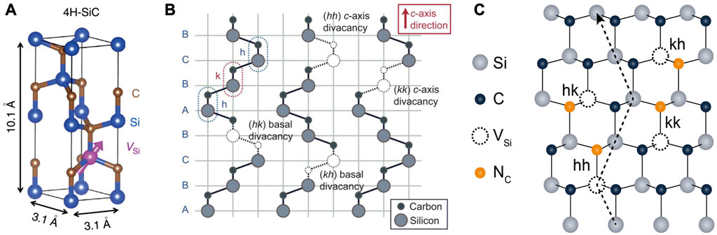
FIGURE 1. Atom configurations of the three main types of spin defects in silicon carbide. (A) Silicon-vacancy center [20], reprinted with permission from Macmillan Publishers Ltd.: Nature Communications [20], copyright (2015). (B) Divacancy center [15], reprinted with permission from Macmillan Publishers Ltd.: Nature [15], copyright (2011). (C) Nitrogen-vacancy centers [24], reprinted with permission from AAAS.
All three types of spin defects have achieved efficient fabrication of single spin and have been applied in various quantum technology applications [15, 16, 22], including integrated quantum photonics [18, 25], quantum information processing [15–17], quantum networks [26, 27], and quantum sensing [24]. In quantum photonics, nanopillars [25] and solid immersion lenses [17] have been used to enhance the silicon-vacancy center count several times. Photonic crystal cavities realize an 80-fold selective Purcell enhancement of the zero-phonon line (ZPL) for silicon-vacancy centers [28]. Most recently, the silicon carbide-on-insulator on-chip integrated nanophotonic cavity has efficiently enhanced the emission of a single silicon-vacancy center and the frequency conversion [29]. Moreover, silicon-vacancy centers can be integrated into nano-fabricated waveguide devices. In addition, the photonic crystal cavity also realizes a 50-fold Purcell enhancement of a single divacancy center [30]. In the quantum information process, coherent control of single silicon-vacancy and divacancy centers has been realized, demonstrating their longer coherence times of approximately 1 ms [16, 17]. The coherence time of divacancy centers has been extended to greater than 5 s using the dynamical decoupling methods and an isotopically purified SiC sample [31]. High-fidelity nuclear quantum registers have been demonstrated using a single silicon-vacancy center [32] and divacancy center [33]. The spin defects have advantages in long-distance quantum networks for their near-infrared fluorescence [26, 27, 34, 35]. A high-fidelity spin-photon interface has been realized in a single silicon-vacancy center [26] and divacancy center [27, 34, 35]. Moreover, the charge depletion technology has been found to narrow optical linewidths by more than 50-fold, approaching the lifetime limit [34]. Optical Rabi oscillations of single divacancy centers have also been realized [35]. All three spin defects have been widely used in high-sensitivity multiple quantum sensing, including magnetic field [36], electric field [37], temperature [38], strain [39], and pressure [40].
Given the rapid development of SiC-based quantum technologies, in this review, we discuss recent progress in the fabrication and quantum sensing of spin defects in SiC. We begin by focusing on the advances in single and ensemble fabrication methods of the three spin defects. Then, we discuss the achievements of the SiC-based multiple quantum sensing applications under atmospheric environments and high pressure. Finally, the conclusions and outlook of SiC spin defect fabrication and quantum sensing are discussed.
Spin defects in SiC, such as the silicon-vacancy center, divacancy center, and nitrogen-vacancy centers, exhibit excellent spin and optical properties for quantum technologies [41–43]. Efficient and controllable fabrication technologies are very important to fully realize their potential in various SiC-based quantum technologies. In this section, we first review the progress in the fabrication of three spin defects in SiC, respectively. Currently, four methods, including electron or neutron irradiation [17, 20], ion implantation [44, 45], focused ion beam implantation [46, 47], and laser writing [48], have been used in the fabrication of three types of spin defects in SiC.
The silicon-vacancy center is a paramagnetic defect consisting of a missing silicon atom in the SiC lattice [17, 20]. The negatively charged silicon-vacancy center has the spin state S = 3/2. There are two types of silicon-vacancy centers in 4H–SiC: V1 and V2, and their corresponding ZPLs are 861 nm (V1) and 915 nm (V2), respectively [17, 20, 44–46]. There are three types of silicon-vacancy centers in 6H–SiC, the ZPLs of which are at 865 nm (V1), 887 nm (V2), and 908 nm (V3), respectively [49]. Due to its spin state, which can be coherently controlled at room temperature, the V2 in 4H–SiC has become the most studied type of silicon-vacancy center [17, 20, 44–46]. The zero-field-splitting D of V2 is 35 MHz.
In order to isolate single silicon-vacancy centers, most of the experiments use commercially available high-purity SiC samples [17, 20, 44–46]. High-energy electron and neutron irradiations are used to generate single silicon-vacancy centers, and a confocal scanning microscopy image is shown in Figure 2A [17]. This method can generate silicon-vacancy centers throughout the sample. Particularly, F. Fuchs et al. used neutron irradiation (0.18 MeV–2.5 MeV) in a fission reactor to generate single silicon-vacancy centers [20]. The irradiation dose is varied over more than eight orders of magnitude, from 1 × 10⁹ to 5 × 1017 cm−2. The single silicon-vacancy center can be observed at the level of 1 × 109 cm−2.
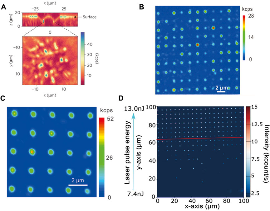
FIGURE 2. Confocal images of silicon-vacancy centers on SiC by using different methods. (A) PL confocal map of irradiation on 4H–SiC using 2 MeV electrons after annealing [17], reprinted with permission from Macmillan Publishers Ltd.: Nature Materials [17], copyright (2015). (B) PL image of the ion implantation confocal map after annealing at 600°C for 1 h [45], copyright (2019), American Chemical Society. (C) PL image of focused ion implantation using Si2+ [46], copyright (2017), American Chemical Society. (D) PL image of laser writing at an energy from 7.4 to 13 nJ [48], copyright (2019), American Chemical Society.
Compared to irradiation, ion implantation allows color centers’ predetermined location fabrication [44, 45]. Carbon, hydrogen, and helium ions are demonstrated to generate shallow single silicon vacancies over a wide dose ranging from 1011 cm−2 to 1014 cm−2. With the same energy, helium ions have better implantation conversion efficiency than carbon and hydrogen ions [45]. After using the optimized annealing, the conversion yield can be further increased more than 2 times. High-concentration silicon ensemble defects contribute to higher sensitivity in magnetic or temperature sensing [45]. To generate single silicon-vacancy center arrays, a polymethyl methacrylate (PMMA) layer, usually several hundred nanometers thick, should be deposited on the SiC surface by spin coating. Electron-beam lithography (EBL) is then employed to make an array of apertures with a specific separation [44]. Then, holes are made before ion implantation. The stopping and range of ions in matter (SRIM) simulation shows that carbon atoms can be blocked by the PMMA layer, which leads to the generation of defects only in the SiC layer below the holes of PMMA layer. By contrast, 20 keV helium and hydrogen ions can penetrate through the 200-nm PMMA layer. After implantation, the PMMA layer is removed in acetone, and the apertures are also cleaned by isopropanol ultrasonication. By using 30 keV carbon ions, the single defect generation ratio is approximately 34% ± 4%, and the conversion yield of the implanted carbon ions into the silicon-vacancy defects is approximately 19% ± 4% [44]. Furthermore, by adding the annealing process (temperature at 600°C for 1 h), the conversion yield can be improved to approximately 78% ± 5%, which is approximately four times higher than unannealed results and leads to less residual radiation damage [45]. Figure 2B shows the confocal image of the silicon-vacancy center array after annealing. This method can realize the on-demand generation of single silicon-vacancy centers [45]. However, since the ion implantation creates residual radiation damage, this method may degrade its effect on the coherence properties of silicon-vacancy centers.
As is mentioned in ion implantation, the determination of the location needs a PMMA mask, making it inconvenient to integrate with photonic devices [46, 47, 50]. Focused ion beam (FIB) implantation provides a method for three-dimensional silicon-vacancy center engineering, which needs no mask, and vacancies are generated by ion collision [46, 47]. The depth of defects is determined and can be predicted by SRIM simulation based on the ion energy and the relationship between the ion energy loss in a particular implanted material and the depth of implantation, while the lateral distribution is controlled by the focused ion beam with nanometer resolution implemented by predesigned computer files [46, 47]. The focused ion spot scale is a nanometer, and the implantation dose that determines the vacancy number can be precisely controlled by the beam current and the residence time [17]. So far, there are hydrogen (H+, 1.7 MeV) [47], silicon (Si2+, 35 keV) [46], and helium (He2+, 30 keV with a dose of 1×1013 cm-2) [50] ions used in focused ion beam implantation. The Si2+ and He2+ implantations need the annealing process to restore the lattice damage caused by implantation at 650°C in air for 6 h and 500°C for 2 h in a vacuum, respectively. In addition, in the He2+ ion implantation process, post-annealing at 600°C in vacuum is adopted to remove the interstitial defects and reduce background fluorescence. Figure 2C presents the PL confocal scan of focused Si2+ beam implantation. By optimizing the dose at 20 ions per spot, focused He2+ and Si2+ ion beam implantation can achieve a conversion yield of approximately 6.95% and 3.9% and a generation rate for a single silicon-vacancy center of approximately 35% and 38%, respectively [46, 50].
All the aforementioned methods inevitably cause residual damage to the lattice, which may degrade the defects’ optical and spin properties. Femtosecond (fs) laser writing minimizes the damage to the crystal lattice and is convenient to realize on-demand location vacancy center generation in 4H–SiC and 6H–SiC [48, 51, 52]. A femtosecond pulsed laser with a central wavelength of 790 nm and a duration time of 250 fs is used [48]. An objective is used to focus the laser beam onto the sample that is fixed on the three-dimensional highly precise translation stage. Before laser writing, samples need to be cleaned using Piranha solution to remove organic contaminants [18–20]. Generally, the separation between arrays is 5 μm, and laser energy from several to hundreds of nanojoules is performed per pulse for each line. Figure 2D shows the confocal image after different energy laser writing. Experimental results get an optically stable single VSi yield of up to 30% and a lateral position accuracy of 80 nm without post-annealing, which is sufficient for coupling VSi centers to optical structures, such as multi-mode waveguides, solid immersion lenses, or nanopillars. However, to enhance the photostability and yield, an extra annealing process can be employed. Moreover, the pulse laser can also be used to ablate 4H–SiC nanoparticles with silicon-vacancy centers [53].
Divacancy centers in SiC consist of a missing Si atom adjacent to a missing C atom, and the neutrally charged divacancy centers have spin state S = 1 [15, 16]. Divacancy centers exist in three polytypes of SiC: 4H–, 6H–, and 3C–SiC [15, 16, 54]. There are seven types of divacancy centers in 4H–SiC, named PL1–PL7. Similarly, there are also six types of divacancy centers in 6H–SiC, named QL1–QL6. There is only one type of divacancy center in 3C–SiC. Since the ODMR contrast and coherence time of the divacancy centers in 4H–SiC are larger than those of divacancy centers in 6H–SiC, most experiments focus on the divacancy centers in 4H–SiC [15, 16, 54]. The basic method for generating divacancy centers by irradiation is the same as for generating silicon-vacancy centers. Using 2 MeV electrons with a dose ranging from 5 × 1012 cm−2 (for generation single divacancy centers) to 1 × 1015 cm−2 to generate Si and C vacancies uniformly, followed by annealing at 750°C or 850°C (for neutral VV0) for 30 min in Ar gas, enables Si and C vacancies to migrate and form divacancies [16, 27]. As shown in Figures 3A, 3B, this method has been used to generate single divacancy centers in 4H– and 3C–SiC [16, 27]. However, the position of the divacancy center is random.
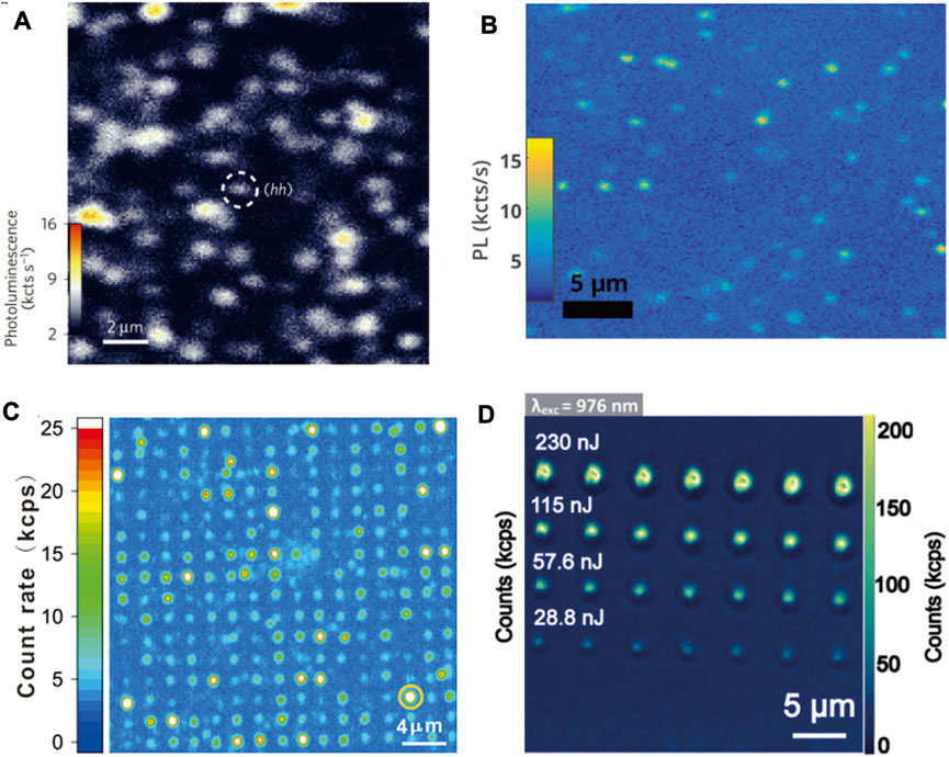
FIGURE 3. Confocal images of divacancy centers on SiC by using different methods and materials. (A) Irradiation at 1013 cm−2 fluence at a depth of 20 µm into the 4H–SiC membrane [16]. Not all spots are isolated single defects, reprinted with permission from Macmillan Publishers Ltd.: Nature Materials [16], copyright (2015). (B) PL scan of 3C–SiC by irradiation [27], copyright (2017), American Physical Society. (C) 30 keV carbon ion implantation on 4H–SiC [55], copyright (2021), China Science Publishing & Media Ltd. (D) Laser writing PL confocal image. No dots are observed under 28.8 nJ [56], reprinted with permission from Almutairi AFM et al., Copyright (2022), AIP Publishing LLC.
Similar to silicon-vacancy center generation using ion implantation, divacancy centers can be fabricated in the same way. A 200-nm-thick positive electron-beam photoresist PMMA layer is spin-coated onto the sample surface. EBL is performed to create a mask, on which an array of apertures with a separation distance of 2 μm and a diameter of 50 ± 10 nm are produced [55]. 30 keV C+ with a dose of 1.02 × 1015 cm−2 are implanted, making approximately 20 ions per spot. The results are shown in Figure 3C. After removing the mask in acetone solution with an ultrasonic bath, the sample is annealed at 900°C for 30 min in vacuum [55]. To reduce background fluorescence, the sample was cleaned again in a mixture of concentrated sulfuric acid and hydrogen peroxide with a ratio of 3:1 [23]. This method generates different types of divacancy centers. The coherent manipulation of single PL6 divacancy center spins in 4H–SiC with a high readout contrast (30%) and a high photon count rate (150 kcps) at room temperature is demonstrated [55]. The coupling between a single divacancy spin and a nearby silicon nuclear spin is also observed.
As divacancy centers generated by electron irradiation are randomly distributed, ion implantation with a PMMA mask causes residual lattice damage, and shallow color centers limit some applications, laser writing is adopted. Using a high-purity 4H–SiC sample as the host material, with a laser wavelength of 1,030 nm, and writing in an argon atmosphere [56], the procedure for generating divacancy centers is the same as that for silicon-vacancy centers. As presented in Figure 3D, divacancy centers in the same row are formed with the same laser energy of 230, 115, 57.7, and 28.8 nJ, respectively [56]. The post-annealing method is performed from 500°C to 1,000°C in a step of 100°C for 30 min in argon gas. Results show that the optimized annealing temperature is 800 °C [56].
The NCVSi center in SiC consists of a nitrogen impurity substituting a carbon atom (NC) and a silicon vacancy (VSi) adjacent to it [21–24]. It can be observed in three polytypes of SiC: 4H–, 6H–, and 3C–SiC [21–24, 57, 58]. The negatively charged state NV center has a spin state of 1. In n-type 4H–SiC, 12 MeV proton irradiation with a dose of 1 × 1014 cm-2 and post-annealing at 900°C can create NV centers [21]. High-energy protons and electrons can cause point defects, while heavy ions generate large residual lattice damage [21]. Except for n-type 4H–SiC with a nitrogen concentration of 1018 cm−3, high-purity semi-insulting 4H–SiC (nitrogen concentration = 3 × 1015 cm−2) is also used in NV center generation. Various ions, such as 240 keV hydrogen, 2 MeV nitrogen, 4 MeV silicon, and 7 MeV iodine ion beams, are utilized for irradiation to generate the NV center ensemble, as shown in Figure 4A [59]. Then, all samples are annealed in Ar gas (1 × 10⁵ Pa) at different temperatures for 30 min and naturally cooled down to room temperature. Results show that 1,000°C is the optimal annealing temperature to generate NV centers [59].
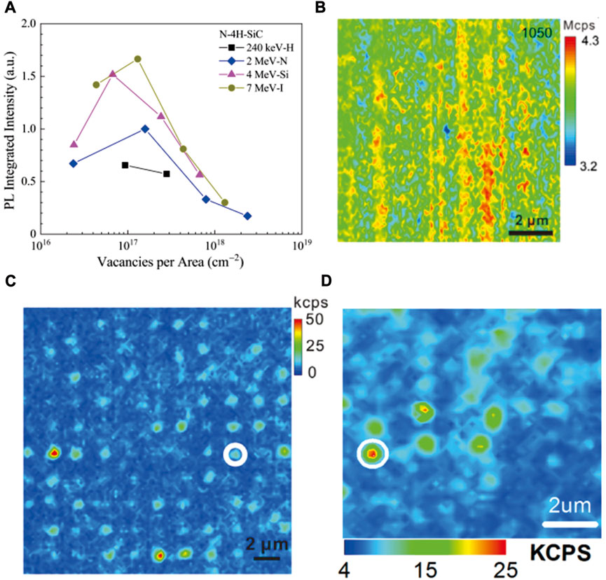
FIGURE 4. Confocal images of NV centers in 4H–SiC by using different methods and calculations of PL integrated intensity as a function of vacancy centers per area. (A) PL integrated intensity of the NV centers as a function of vacancy centers per area [59], reprinted with permission from Sato SI et al., Copyright (2019), AIP Publishing LLC. (B) PL images of the NV center ensemble by carbon ion implantation after annealing at 1,050°C [22], copyright (2020), American Physical Society. (C) Confocal scan image of the single NV center array [22], copyright (2020), American Physical Society. (D) Confocal scan image of single NV centers at a low dose (1010/cm2) [23], copyright (2020), American Chemical Society.
In addition, as shown in Figure 4B, 30 keV nitrogen ion implantation (dose 1 × 1014 cm−2) can create shallow single NV center ensemble at a depth of 60 nm in a bulk high-purity 4H–SiC epitaxy layer sample. After annealing under optimal conditions at 1,050°C for 2 h, NV centers’ concentration can increase by six times. Using the masked implantation methods, the single NV center array is generated. Figures 4C, 4D show confocal images of the single NV center array by nitrogen ion implantation. The single defect generation efficiency is around 30%, and the conversion yield of the implanted nitrogen ions into the NV center is approximately 4.3% [22]. The NV centers are proven as a three-energy-level electronic structure system. Both the excitation and the emission polarization degrees are approximately 90% for c-axis NV centers [60].
Color centers in SiC have been applied to various quantum sensing fields, such as magnetic field, electric field, temperature, strain, and pressure [36–40]. They have some advantages, including high sensitivity and high spatial resolution under ambient conditions. Combined with mature micro- and nano-fabrication and growth technologies of SiC, SiC color center-based quantum sensing will have widespread applications [36–40]. Figure 5 shows the Hamiltonian of the spin defects’ spin state and their relevant physical parameters [3, 61, 62]. The spin state S is 1 for the divacancy and NV centers in SiC, and it is 3/2 for the silicon-vacancy centers in SiC. The electron gyromagnetic ratio γ is 2.8 MHz/G. The first item is zero-field splitting (ZFS), and D is related to temperature and pressure, which can be used for temperature sensing and pressure sensing [3, 62]. The second item is the Zeeman splitting, which can be used for magnetic field sensing, and the last item is the Stark effect, which can be used for electric field and strain [3, 62]. We then discuss the progress of these various quantum sensing methods in detail.
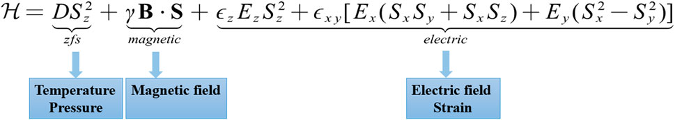
FIGURE 5. Spin Hamiltonian of the spin defects in SiC and related quantum sensing physical quantities for each term of the Hamiltonian.
Since these color centers in SiC are spin defects, one of the main quantum sensing is magnetic field sensing through measuring the Zeeman splitting [36]. SiC offers a platform for wafer-scale quantum sensing at room temperature, benefiting from its mature fabrication and generation technologies. Continuous wave ODMR is the most useful and simplest magnetic field detection method [36, 63–66]. The ODMR magnetic field sensitivity is [63]
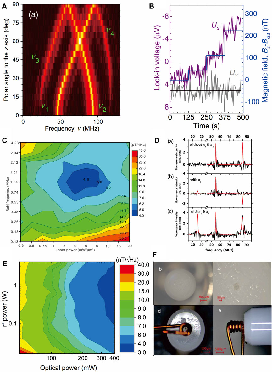
FIGURE 6. Magnetometry sensitivity maps and set-up images. (A) Experimental results of the angle evolution of Vsi ODMR spectra under an external magnetic field of B = 0.8 mT [66], copyright (2015), American Physical Society. (B) Lock in signal in-phase Ux and quadrature Uy as a function of sub-μT magnetic fields. The magnetic field increases in the sub-μT level every 125 s [68], copyright (2016), American Physical Society. (C) The magnetometry sensitivity as a function of laser power and Rabi frequency [64], copyright (2020), American Physical Society. (D) Pulsed ODMR spectra in the same magnetic field and at the same angle but using different pulse sequences. (a) Sweep pulse. (b) A π pulse before the sweep pulse. (c) A π pulse before and after the sweep pulse [36], copyright (2016), American Physical Society. (E) The shot-noise-limited sensitivity map in magnetometry after thermal quenching [65], copyright (2021), American Physical Society. (F) Images of the fiber-integrated probe. The probe consists of a multi-mode fiber tip, a copper wire, and a SiC sample pasted on the fiber tip. b, c, d, and e are pictures of the probe at different angles [69], copyright (2023), Optica Publishing Group.
The linewidth of the ODMR is fundamentally limited by the dephasing time T2∗ of the spin defects [63]. The laser- and MW-dependent power broadening also affects the ODMR linewidth [63, 64]. Increasing the ODMR contrast and decreasing the ODMR linewidth will generate higher sensitivity. Wang J. F. et al. investigated the ODMR contrast and linewidth as functions of laser power and the microwave (MW) power of the divacancy center at room temperature [64]. The results show that the ODMR contrast decreases with the laser power, while the ODMR linewidth only slightly increases as the laser power increases [64]. Both the ODMR contrast and the linewidth increase with the MW power. Finally, they present a two-dimensional experimental magnetic field sensitivity image as a function of laser and MW power as shown in Figure 6C. The sensitivity increases by approximately 10 times (4 μT/Hz1/2) for the optimized laser and MW power range [64]. In order to further decrease the linewidth of the ODMR, the pulsed ODMR spectra are used in the experiments as shown in Figure 6D [36]. The linewidth can be reached at approximately 500 kHz, which causes a sensitivity of 200 μT/Hz1/2 [36].
The ODMR contrast is one of the main factors limiting the SiC defects’ sensitivity. Recently, a study found that the ODMR contrast and count rate can increase approximately ten and two times by using thermally quenched methods as shown in Figure 6E [65]. After optimizing the laser and microwave power broadening of the ODMR, the experimental sensitivity can increase to approximately 3.5 nT/Hz1/2 [65]. However, all the previous magnetometers use the confocal system, which is not suitable for applications in practical environments. To further increase the capability of the magnetometer and make it compatible with practical environments, it needs to integrate the silicon-vacancy center-based magnetometer with optical fiber [69, 70]. SiC is a technology-friendly semiconductor material, which has mature growth and fabrication techniques. SiC-based magnetic field sensing is compatible with the semiconductor industry and could be widely used. Moreover, since the wavelengths of the spin defects in SiC are near-infrared, they are useful for long-distance magnetometry. Quan W. K. et al. realized the fiber-integrated SiC-based magnetometer [69, 70]. As shown in Figure 6F they pasted a pasted a 100-µm-diameter sample on a fiber tip and realized an efficient coupling of the silicon-vacancy and divacancy centers with the fiber. After optimizing the laser and MW powers broadening the linewidth of ODMR peaks, they obtained a sensitivity of 12.3 μT/Hz1/2 and 3.9 μT/Hz1/2, respectively [69, 70]. It has been used to sense external magnetic field strength and angle.
The basic principle of SiC-based temperature sensing is that the ground zero-field-splitting (ZFS) D of the divacancy center decreases with the temperature [38, 71, 72]. The three types of divacancy centers’ D parameters in 4H–SiC decrease when the temperature increases, and PL5 and PL6 divacancy centers’ ZFS linearly decrease around room temperature with a slope of approximately −109.5 and 100 kHz/Hz1/2 as shown in Figure 7A, respectively. Those values are approximately 1.5 times larger than that of the NV centers in diamond [38, 73]. On this basis, the Ramsey methods have been used to measure the temperatures and the results are shown in Figure 7B. The dephasing time T2* is approximately 2 μs, and it does not change as the temperature decreases from 300 K to 20 K [38]. The change of the Ramsey oscillation frequency is due to the change of the temperature, which can be used for temperature sensing. The sensitivity is
where
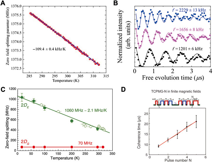
FIGURE 7. ODMR, Ramsey, and TCPMG measurements under different temperatures. (A) ODMR resonant frequency as a function of temperature [38]. The blue line is a linear fitting to the data, copyright (2017), American Physical Society. (B) Ramsey oscillation under three representative temperatures [38], copyright (2017), American Physical Society. (C) The ground-state (GS) and excited-state (ES) ZFS as a function of temperature [77], reprinted with permission from Macmillan Publishers Ltd.: Scientific Reports [77], copyright (2016). (D) The TCPMG-N pulse sequences and corresponding coherence time experimental results [73], copyright (2023), the Royal Society of Chemistry.
Except for the ground-state ZFS, the excited-state ZFS can also be used for temperature sensing [77, 78]. The ground-state ZFS of the silicon-vacancy centers in SiC does not change as the temperature decreases from 320 K to approximately 20 K, which is due to Kramers’ theorem [76, 77, 79]. The half-integer spin system is insensitive to fluctuations in strain, temperature, and electric field [79]. However, as shown in Figure 7C, the excited-state ZFS is found to have a large thermal shift of 2.1 MHz/K in 4H–SiC, and the sensitivity is approximately 100 mK/Hz1/2 [77]. Combined with the 4H–SiC p–n diode using proton beam writing, the temperature change induced by an injected current is measured [78]. The results pave the way for practical applications inside SiC power devices like thermometers. In order to further increase the sensitivity, the coherence time needs to be further increased. The thermal Carr–Purcell–Meiboom–Gill (TCPMG) methods are performed on the PL6 divacancy center at room temperature [73]. As shown in Figure 7D, the coherence time linearly increases with the pulse numbers, and the longest coherence time is approximately 21 μs, which is 10 times higher than T2*. The corresponding sensitivity is 13.4 mK/Hz1/2, which is approximately 15 times higher than that of the Ramsey results [73]. In order to apply the SiC-based thermometer to practical environments, fiber-coupled PL5 divacancy center thermometers are prepared. A 100-μm-diameter SiC with divacancy centers is pasted on the fiber tips. The ODMR and Ramsey methods are used for wide-range and highly precise temperature sensing, respectively. The sensitivity can reach approximately 163 mK/Hz1/2 [70].
The basic principle of electric field sensing of spin defects in SiC is the Stark effect. For divacancy centers, their Hamiltonian (the defects are z-axis) is as follows [39]:
where h is Planck’s constant; D, Ex, and Ey are the zero-magnetic-field splitting parameters, g is the electron g factor, μB is the Bohr magneton, B is the magnetic field, and σ is the vector of spin-1 Pauli matrices. D can be written as
In order to detect the AC electric field, the ± Vmem pulses are applied across a 53-μm-thick SiC membrane sample with divacancy centers (see Figure 8A). The Hahn-echo pulse scheme is used for T2-limited AC electric field sensing [39]. During the free evolution periods, Vmem pulses can cause an electric field-induced phase shift of the spin superposition. Five types of divacancy centers, including both basal and c-axis-oriented, are used to measure the electric field both at 20 K and 300 K [39]. The fits use exponentially decaying sine curves, and fitted frequencies are spin–electric field coupling parameters. Experimentally measured and calculated Stark parameters for the PL1–PL6 ground-state-spin Hamiltonians in 4H–SiC are shown in Table 1.
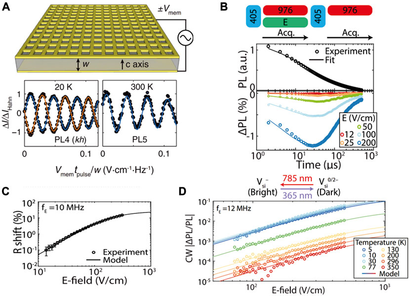
FIGURE 8. Experimental setup and measurements under different electric fields. (A) Schematic of the SiC sample and the voltage applied on the sample for electric field measurement (upper part) and experimental results by utilizing the pulse sequence (lower part) [39], copyright (2014), American Physical Society. (B) Pulse sequence used in measurement (upper part) and the normalized PL at different electric fields (lower part) [37], reproduced from [37], CC BY 4.0. (C) R shift as a function of the electric field. The points are experimental results, and the black line is the fitting by using the model [37], reproduced from [37], CC BY 4.0. (D) EOCC contrast as a function of the electric field under different temperatures by using silicon-vacancy centers [37], reproduced from [37], CC BY 4.0.
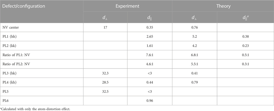
TABLE 1. Experimentally measured and calculated Stark parameters for the PL1–PL6 ground-state-spin Hamiltonians in 4H–SiC [39], copyright (2014), American Physical Society.
Except for the spin methods, all-optical method electrometry is also realized. The optical charge conversion (OCC) rate between the bright and dark charge states of both divacancy and silicon-vacancy centers is strongly modulated by the applied microwave (megahertz to gigahertz) electric field and, therefore, can be used to detect the electric field through changes in photoluminescence (PL). G. Wolfowicz et al. characterized OCC transient decays by resetting the charge state with 405 nm illumination followed by a 976-nm pump laser (pulse sequence is shown at the top of Figure 8B) [37]. As shown in Figure 8B, the decay can be fitted by an exponential decay function: f(t) is exp (−(Rt)n), where R is the decay time. The electric field-induced changed R is
Electrical field and strain interactions with spin defects are intertwined, so the spin defects can also be used to detect the strain. The D and Ex,y in Eq. 2 are also related to strain as follows:
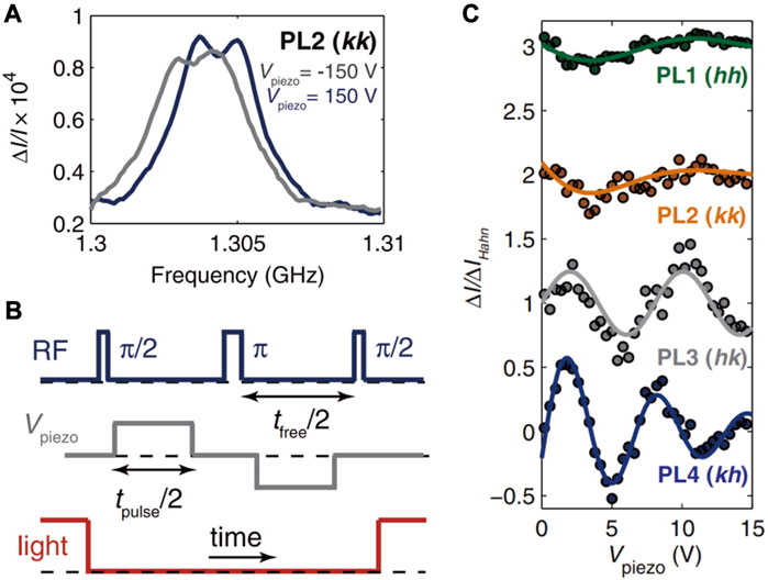
FIGURE 9. ODMR measurements and Hahn-echo pulse sequence and corresponding results. (A) DC ODMR results for strain sensing at a temperature of 20 K. By utilizing the opposite voltage, a 0.8 MHz shift is observed [39], copyright (2014), American Physical Society. (B) The Hahn-echo pulse sequence used to measure the strain [39], copyright (2014), American Physical Society. (C) Hahn-echo results for PL1–PL4 without external magnetic field [39], copyright (2014), American Physical Society.
Strain also affects the spin states. Transverse strain shifts the ODMR of the PL2 for approximately 0.8 MHz, with a 300 V piezo value [39]. The DC strain sensing is limited by T2*, which is the inhomogeneous spin-dephasing time (approximately 1.5 μs). It can also be used to detect AC strain. The Hahn-echo pulse scheme is used for T2-limited AC strain sensing, as shown in Figure 9B. The corresponding AC strain sensing data are shown in Figure 9C.
High-pressure technologies have been widely applied in physics, geophysics, and material sciences, inducing many unusual and important phenomena at high pressures [81–83]. In the last few decades, pressure-induced high-critical-temperature (Tc) superconductivity has drawn much attention [82, 83]. For example, the Tc of lanthanum hydride increases to 250 K at 170 GPa [82, 83]. However, measuring the local magnetic field in the diamond anvil cell (DAC) is still a great challenge due to the micrometer-sized sample chamber [84–87]. It is important to generate new methods to overcome the challenges. The ZFS of the NV centers linearly increases with a slope of 14.6 MHz/GPa at high pressure [88]. Using the ODMR of the NV centers in diamond, the pressure-induced magnetization of the Fe particles and the Meissner effect of superconductors have been measured [84–87]. However, the NV centers have four axes, and their ZFS decreases with temperature, which makes it a little difficult to analyze the ODMR spectra [84–87]. Similar to NV centers in diamond, defects in silicon carbide (SiC) could also be used to measure the magnetic properties of materials at high pressure [40, 89]. SiC is a widely used semiconductor, which has mature inch-scale growth and micro/nano-fabrication technologies.
The silicon-vacancy center in SiC has only a single axis, and the ODMR has only two resonant peaks at an external magnetic field. Moreover, it also has a temperature-independent ZFS. The two superior properties make it convenient to analyze the ODMR spectra [40, 76]. Recently, Wang J. F. et al. realized a magnetic detection under high pressures using designed silicon-vacancy centers in SiC [40]. As presented in Figure 10A, two high-quality single-crystal 4H-SiC cubes are used to fabricate SiC anvils with 200-µm-diameter culets. A 100-nm-deep high-density shallow silicon-vacancy center is generated (20keV He implantation) for magnetic detection. The ZFS increases with the pressure with a slope of 0.31 MHz/GPa (Figure 10B), which is obviously smaller than the coefficient of 14.6 MHz/GPa for NV centers in diamond. The coherence time T2 remains invariable up to 25 GPa. Then, a tiny Nd2Fe14B sample is placed on the culet surface, and using the ODMR of the shallow silicon-vacancy centers, the pressure-induced magnetic phase transition is observed and presented in Figure 10C. The phase transition range is from 6 GPa to 10 GPa, which is consistent with previous results [87]. Finally, they used the ODMR methods to measure the Meissner effect of a well-known superconductor YBa2Cu3O6.6 (Figure 10D) and map the Tc–pressure phase diagram. The Tc increases as the pressure increases to approximately 17.1 GPa (Figure 10E), which is consistent with the results obtained by AC susceptibility methods in the DAC [40]. The experiments prove that the silicon-vacancy center is an excellent quantum sensor at high pressure.
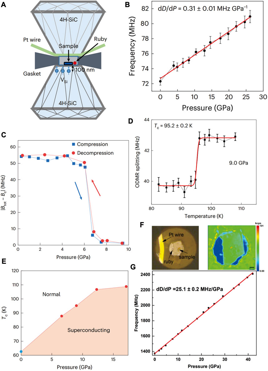
FIGURE 10. (A) Schematic of the SiC anvil cell [40], reprinted with permission from Macmillan Publishers Ltd.: Nature Materials [40], copyright (2023). (B) The D shifts under different pressure. The red line shows that the D value has a linear dependence on pressure [40], reprinted with permission from Macmillan Publishers Ltd.: Nature Materials [40], copyright (2023). (C) The magnetometry of the Nd2Fe14B sample by using silicon-vacancy centers under compression (blue) and decompression (red) processes, respectively [40], reprinted with permission from Macmillan Publishers Ltd.: Nature Materials [40], copyright (2023). (D) ODMR splitting as a function of temperature under 9.0 GPa. The mutation point shows the superconducting transition [40], reprinted with permission from Macmillan Publishers Ltd.: Nature Materials [40], copyright (2023). (E) The YBa2Cu3O6.6 phase diagram [40]. By measuring Tc under different pressures, the Tc–pressure phase diagram can be obtained. The orange part is in the superconducting phase, and the white part is in the normal state, reprinted with permission from Macmillan Publishers Ltd.: Nature Materials [40], copyright (2023). (F) Optical image of the culet surface (left) and the fluorescence scanning confocal image of the sample (right), respectively [89], copyright (2022), American Chemical Society. (G) The D shift as a function of pressure. The red line is a linear fitting to the data [89], copyright (2022), American Chemical Society.
Divacancy centers can also be used in quantum sensing at high pressure. As shown in Figure 10F, a tiny SiC sample with high-concentration divacancy centers is placed in the DAC chamber. The ZPLs of the PL5 and PL6 are also blueshifted with pressure. The ZFS D of the PL5, PL6, and PL7 linearly increases with pressure with coefficients of 25.1, 11.8, and 23.6 MHz/GPa, respectively (Figure 10G). The ZFS E of PL5 values keep stable at 17 MHz as the pressure increases to 8 GPa. The ODMR contrast decreases with the pressure. The pressure sensing sensitivity of the divacancy center ensemble at room temperature is
In this review, we focused on the fabrication of three spin defects and various quantum sensing of the spin defects in SiC. We first summarize four main methods used to generate the three spin defects: electron or neutron irradiation, ion implantation, focused ion implantation, and laser writing, discussing the specific advantages of the efficiency and position accuracy of these methods. On this basis, we discuss the progress in various quantum sensing fields, including magnetic field, temperature, electric field, strain, and high pressure. We introduce the basic working principles, sensing sensitivities, and spatial resolutions of these quantum sensing methods.
Because of the low counts of the single-spin defects, one of the challenges in spin defect fabrication is the on-demand generation with high spatial accuracy, which will be beneficial for coupling with the photonic structures. For quantum sensing, there are some methods to further increase the sensitivity. The first one is using photonic structures, such as nanopillars [25], solid immersion lenses [17], ring resonators, and photonic crystal cavities [29], to increase the counts of the spin defects. The second is using the isotope purification SiC sample or dynamical decoupling methods to increase the coherence time [31]. The third is optimizing the generation method to increase the concentration of spin defects. Combining nano SiC samples with an atomic force microscope (AFM), spin defects can be used to realize nanoscale quantum sensing imaging [53, 90]. Various SiC spin defect-based quantum sensing have high sensitivity and spatial resolution, opening up wide applications in physics, biology, and materials science. With the progress of this technology, quantum sensing will extend the range of applications and make them more feasible in practical environments.
Q-YL: Writing–original draft, Writing–review and editing. QL: Writing–original draft, Writing–review and editing. J-FW: Writing–original draft, Writing–review and editing, Funding acquisition, Supervision. P-JG: Writing–original draft. W-XL: Writing–original draft. SZ: Writing–original draft. Q-CH: Writing–original draft. Z-QZ: Writing–original draft. J-SX: Writing–original draft, Writing–review and editing, Funding acquisition, Supervision. C-FL: Writing–original draft, Writing–review and editing, Funding acquisition, Supervision. G-CG: Writing–review and editing, Supervision.
The authors declare financial support was received for the research, authorship, and/or publication of this article. This work was supported by the Innovation Program for Quantum Science and Technology (Grant No. 2021ZD0301400), the National Natural Science Foundation of China (Grant Nos. 11975221, 61905233, U19A2075, and 11821404), Anhui Initiative in Quantum Information Technologies (Grant No. AHY060300), and the Fundamental Research Funds for the Central Universities (Grant No. WK2470000026).
J-FW also acknowledges financial support from the Science Specialty Program of Sichuan University (Grant No. 2020SCUNL210).
The authors declare that the research was conducted in the absence of any commercial or financial relationships that could be construed as a potential conflict of interest.
The authors declare that they were editorial board members of Frontiers, at the time of submission. This had no impact on the peer review process and the final decision.
All claims expressed in this article are solely those of the authors and do not necessarily represent those of their affiliated organizations, or those of the publisher, the editors, and the reviewers. Any product that may be evaluated in this article, or claim that may be made by its manufacturer, is not guaranteed or endorsed by the publisher.
1. Zhang G, Cheng Y, Chou JP, Gali A. Material platforms for defect qubits and single-photon emitters. Appl Phys Rev (2020) 7:31308. doi:10.1063/5.0006075
2. Atatüre M, Englund D, Vamivakas N, Lee SY, Wrachtrup J. Material platforms for spin-based photonic quantum technologies. Nat Rev Mater (2018) 3:38–51. doi:10.1038/s41578-018-0008-9
3. Schirhagl R, Chang K, Loretz M, Degen CL. Nitrogen-vacancy centers in diamond: Nanoscale sensors for physics and biology. Annu Rev Phys Chem (2014) 65:83–105. doi:10.1146/annurev-physchem-040513-103659
4. Son NT, Anderson CP, Bourassa A, Miao KC, Babin C, Widmann M, et al. Developing silicon carbide for quantum spintronics. Appl Phys Lett (2020) 116:190501. doi:10.1063/5.0004454
5. Awschalom DD, Hanson R, Wrachtrup J, Zhou BB. Quantum technologies with optically interfaced solid-state spins. Nat Photon (2018) 12:516–27. doi:10.1038/s41566-018-0232-2
6. Gottscholl A, Kianinia M, Soltamov V, Orlinskii S, Mamin G, Bradac C, et al. Initialization and read-out of intrinsic spin defects in a van der Waals crystal at room temperature. Nat Mater (2020) 19:540–5. doi:10.1038/s41563-020-0619-6
7. Berhane AM, Jeong KY, Bodrog Z, Fiedler S, Schröder T, Triviño NV, et al. Bright room-temperature single-photon emission from defects in gallium nitride. Adv Mater (2017) 29:1605092. doi:10.1002/adma.201605092
8. Zhou Y, Wang ZY, Rasmita A, Kim S, Berhane A, Bodrog Z, et al. Room temperature solid-state quantum emitters in the telecom range. Sci Adv (2018) 4:3580. doi:10.1126/sciadv.aar3580
9. Iwasaki T, Miyamoto Y, Taniguchi T, Siyushev P, Metsch MH, Jelezko F, et al. Tin-vacancy quantum emitters in diamond. Phy Rev Lett (2017) 119:253601. doi:10.1103/physrevlett.119.253601
10. Hensen B, Bernien H, Dréau AE, Reiserer A, Kalb N, Blok MS, et al. Loophole-free Bell inequality violation using electron spins separated by 1.3 kilometres. Nature (2015) 526:682–6. doi:10.1038/nature15759
11. Bradley CE, Randall J, Abobeih MH, Berrevoets R, Degen M, Bakker M, et al. A ten-qubit solid-state spin register with quantum memory up to one minute. Phys Rev X (2019) 9:031045. doi:10.1103/physrevx.9.031045
12. Balasubramanian G, Chan IY, Kolesov R, Al-Hmoud M, Tisler J, Shin C, et al. Nanoscale imaging magnetometry with diamond spins under ambient conditions. Nature (2008) 455:648–51. doi:10.1038/nature07278
13. Dréau A, Lesik M, Rondin L, Spinicelli P, Arcizet O, Roch JF, et al. Avoiding power broadening in optically detected magnetic resonance of single NV defects for enhanced dc magnetic field sensitivity. Phys Rev B (2011) 84:195204. doi:10.1103/physrevb.84.195204
14. Balasubramanian G, Neumann P, Twitchen D, Markham M, Kolesov R, Mizuochi N, et al. Ultralong spin coherence time in isotopically engineered diamond. Nat Mater (2009) 8:383–7. doi:10.1038/nmat2420
15. Koehl WF, Buckley BB, Heremans FJ, Calusine G, Awschalom DD. Room temperature coherent control of defect spin qubits in silicon carbide. Nature (2011) 479:84–7. doi:10.1038/nature10562
16. Christle DJ, Falk AL, Andrich P, Klimov PV, Hassan JU, Son N, et al. Isolated electron spins in silicon carbide with millisecond coherence times. Nat Mater (2015) 14:160–3. doi:10.1038/nmat4144
17. Widmann M, Lee SY, Rendler T, Son NT, Fedder H, Paik S, et al. Coherent control of single spins in silicon carbide at room temperature. Nat Mater (2015) 14:164–8. doi:10.1038/nmat4145
18. Lohrmann A, Johnson BC, Mccallum JC, Castelletto S. A review on single photon sources in silicon carbide. Rep Prog Phys Soc (Great Britain) (2017) 80:034502. doi:10.1088/1361-6633/aa5171
19. Wang JF, Zhou Y, Wang ZY, Rasmita A, Yang J, Li X, et al. Bright room temperature single photon source at telecom range in cubic silicon carbide. Nat Commun (2018) 9:4106. doi:10.1038/s41467-018-06605-3
20. Fuchs F, Stender B, Trupke M, Simin D, Pflaum J, Dyakonov V, et al. Engineering near-infrared single-photon emitters with optically active spins in ultrapure silicon carbide. Nat Commun (2015) 6:7578. doi:10.1038/ncomms8578
21. van Bardeleben HJ, Cantin JL, Rauls E, Identification and magneto-optical properties of the NV center in 4H-SiC. Phys Rev B (2015) 92:64104. doi:10.1103/PhysRevB.92.020104
22. Wang JF, Yan FF, Li Q, Liu ZH, Liu H, Guo GP, et al. Coherent control of nitrogen-vacancy center spins in silicon carbide at room temperature. Phys Rev Lett (2020) 124:223601. doi:10.1103/physrevlett.124.223601
23. Zhao M, Soroush AZ, von Bardeleben HJ, Fröch JE, Nonahal M, Cai H, et al. Coherent manipulation with resonant excitation and single emitter creation of nitrogen vacancy centers in 4H silicon carbide. Nano Lett (2020) 20:6142–7. doi:10.1021/acs.nanolett.0c02342
24. Jiang ZZ, Cai HB, Cernansky R, Liu X, Gao W. Quantum sensing of radio-frequency signal with NV centers in SiC. Sci Adv (2023) 9:g2080. doi:10.1126/sciadv.adg2080
25. Radulaski M, Widmann M, Niethammer M, Zhang JL, Lee SY, Rendler T, et al. Scalable quantum photonics with single color centers in silicon carbide. Nano Lett (2017) 17:1782–6. doi:10.1021/acs.nanolett.6b05102
26. Nagy R, Niethammer M, Widmann M, Chen YC, Udvarhelyi P, Bonato C, et al. High-fidelity spin and optical control of single silicon-vacancy centres in silicon carbide. Nat Commun (2019) 10:1954. doi:10.1038/s41467-019-09873-9
27. Christle DJ, Klimov PV, de Las Casas CF, Szász K, Ivády V, Jokubavicius V, et al. Isolated spin qubits in SiC with a high-fidelity infrared spin-to-photon interface. Phys Rev X (2017) 7:021046. doi:10.1103/physrevx.7.021046
28. Bracher DO, Zhang XY, Hu EL, Selective Purcell enhancement of two closely linked zero-phonon transitions of a silicon carbide color center. Proc Natl Acad Sci USA (2017) 114:4060–5. doi:10.1073/pnas.1704219114
29. Lukin Daniil M, Dory C, Guidry MA, Yang KY, Mishra SD, Trivedi R, et al. 4H-silicon-carbide-on-insulator for integrated quantum and nonlinear photonics. Nat Photon (2020) 14:330–4. doi:10.1038/s41566-019-0556-6
30. Crook AL, Anderson CP, Miao KC, Bourassa A, Lee H, Bayliss SL, et al. Purcell enhancement of a single silicon carbide color center with coherent spin control. Nano Lett (2020) 20:3427–34. doi:10.1021/acs.nanolett.0c00339
31. Anderson CP, Glen EO, Zeledon C, Bourassa A, Jin Y, Zhu Y, et al. Five-second coherence of a single spin with single-shot readout in silicon carbide. Sci Adv (2022) 8:eabm5912. doi:10.1126/sciadv.abm5912
32. Babin C, Stöhr R, Morioka N, Linkewitz T, Steidl T, Wörnle R, et al. Fabrication and nanophotonic waveguide integration of silicon carbide colour centres with preserved spin-optical coherence. Nat Mater (2022) 21:67–73. doi:10.1038/s41563-021-01148-3
33. Bourassa A, Anderson CP, Miao KC, Onizhuk M, Ma H, Crook AL, et al. Entanglement and control of single nuclear spins in isotopically engineered silicon carbide. Nat Mater (2020) 19:1319–25. doi:10.1038/s41563-020-00802-6
34. Miao KC, Bourassa A, Anderson CP, Whiteley SJ, Crook AL, Bayliss SL, et al. Electrically driven optical interferometry with spins in silicon carbide. Sci Adv (2019) 5:y0527. doi:10.1126/sciadv.aay0527
35. Anderson CP, Bourassa A, Miao KC, Wolfowicz G, Mintun PJ, Crook AL, et al. Electrical and optical control of single spins integrated in scalable semiconductor devices. Science (2019) 366:1225–30. doi:10.1126/science.aax9406
36. Niethammer M, Widmann M, Lee SY, Stenberg P, Kordina O, Ohshima T, et al. Vector magnetometry using silicon vacancies in 4H-SiC under ambient conditions. Phys Rev Appl (2016) 6:034001. doi:10.1103/physrevapplied.6.034001
37. Wolfowicz G, Whiteley SJ, Awschalom DD. Electrometry by optical charge conversion of deep defects in 4H-SiC. Proc Natl Acad Sci (2018) 115:7879–83. doi:10.1073/pnas.1806998115
38. Zhou Y, Wang JF, Zhang XM, Li K, Cai J, Gao W. Self-protected thermometry with infrared photons and defect spins in silicon carbide. Phys Rev Appl (2017) 8:044015. doi:10.1103/physrevapplied.8.044015
39. Falk AL, Klimov Paul V, Buckley BB, Ivády V, Abrikosov IA, Calusine G, et al. Electrically and mechanically tunable electron spins in silicon carbide color centers. Phys Rev Lett (2014) 112:187601. doi:10.1103/physrevlett.112.187601
40. Wang JF, Liu L, Liu XD, Li Q, Cui JM, Zhou DF, et al. Magnetic detection under high pressures using designed silicon vacancy centres in silicon carbide. Nat Mater (2023) 22:489–94. doi:10.1038/s41563-023-01477-5
41. Lukin DM, Guidry MA, Vučković J. Integrated quantum photonics with silicon carbide: Challenges and prospects. PRX Quan (2020) 1:020102. doi:10.1103/prxquantum.1.020102
42. Castelletto S, Boretti A. Silicon carbide color centers for quantum applications. J Phys Photon (2020) 2:022001. doi:10.1088/2515-7647/ab77a2
43. Yi A, Wang CL, Zhou LP, Zhu Y, Zhang S, You T, et al. Silicon-carbide for integrated photonics. Appl Phys Rev (2022) 9:031302. doi:10.1063/5.0079649
44. Wang JF, Zhou Y, Zhang XM, Liu F, Li Y, Li K, et al. Efficient generation of an array of single silicon-vacancy defects in silicon carbide. Phys Rev Appl (2017) 7:064021. doi:10.1103/physrevapplied.7.064021
45. Wang JF, Li Q, Yan FF, Liu H, Guo GP, Zhang WP, et al. On-demand generation of single silicon vacancy defects in silicon carbide. ACS Photon (2019) 6:1736–43. doi:10.1021/acsphotonics.9b00451
46. Wang JF, Zhang XM, Yu Z, Li K, Wang Z, Peddibhotla P, et al. Scalable fabrication of single silicon vacancy defect arrays in silicon carbide using focused ion beam. ACS Photon (2017) 4:1054–9. doi:10.1021/acsphotonics.7b00230
47. Kraus H, Simin D, Kasper C, Suda Y, Kawabata S, Kada W, et al. Three-dimensional proton beam writing of optically active coherent vacancy spins in silicon carbide. Nano Lett (2017) 17:2865–70. doi:10.1021/acs.nanolett.6b05395
48. Chen YC, Salter PS, Niethammer M, Widmann M, Kaiser F, Nagy R, et al. Laser writing of scalable single color centers in silicon carbide. Nano Lett (2019) 19:2377–83. doi:10.1021/acs.nanolett.8b05070
49. Singh H, Anisimov AN, Breev ID, Baranov PG, Suter D. Optical spin initialization of spin-3/2 silicon vacancy centers in 6H-SiC at room temperature. Phys Rev B (2021) 103:104103. doi:10.1103/physrevb.103.104103
50. He ZX, Li Q, Wen XL. Maskless generation of single silicon vacancy arrays in SiC by a focused He+ ion beam. Washington, DC: ACS Photonics (2023) 10:2234–40. doi:10.1021/acsphotonics.2c01209
51. Castelletto S, Almutairi AFM, Kumagai K, Katkus T, Hayasaki Y, Johnson BC, et al. Photoluminescence in hexagonal silicon carbide by direct femtosecond laser writing. Opt Lett (2018) 43:6077–80. doi:10.1364/ol.43.006077
52. Castelletto S, Maksimovic J, Katkus T, Ohshima T, Johnson BC, Juodkazis S. Color centers enabled by direct femto-second laser writing in wide bandgap semiconductors. Nanomaterials (Basel) (2020) 11:72. doi:10.3390/nano11010072
53. Castelletto S, Almutairi AFM, Thalassinos G, Lohrmann A, Buividas R, Lau DWM, et al. Fluorescent color centers in laser ablated 4H-SiC nanoparticles. Opt Lett (2017) 42:1297–300. doi:10.1364/ol.42.001297
54. Falk AL, Buckley BB, Calusine C, Koehl WF, Dobrovitski VV, Politi A, et al. Polytype control of spin qubits in silicon carbide. Nat Commun (2013) 4:1819. doi:10.1038/ncomms2854
55. Li Q, Wang JF, Yan FF, Zhou JY, Wang HF, Liu H, et al. Room-temperature coherent manipulation of single-spin qubits in silicon carbide with a high readout contrast. Natl Sci Rev (2022) 9:nwab122. doi:10.1093/nsr/nwab122
56. Almutairi AFM, Partridge JG, Chenglong X, Cole IS, Halland AS. Direct writing of divacancy centers in silicon carbide by femtosecond laser irradiation and subsequent thermal annealing. Appl Phys Lett (2022) 120:014003. doi:10.1063/5.0070014
57. Zargaleh SA, von Bardeleben HJ, Cantin JL, Gerstmann U, Hameau S, Eblé B, et al. Electron paramagnetic resonance tagged high-resolution excitation spectroscopy of NV-centers in 4H-SiC. Phys Rev B (2018) 98:214113. doi:10.1103/physrevb.98.214113
58. von Bardeleben HJ, Cantin JL, Csóré A, Gali A, Rauls E, Gerstmann U. NV centers in 3C, 4H, and 6H silicon carbide: A variable platform for solid-state qubits and nanosensors. Phys Rev B (2016) 94:121202. doi:10.1103/physrevb.94.121202
59. Sato SI, Narahara T, Abe Y, Hijikata Y, Umeda T, Ohshima T. Formation of nitrogen-vacancy centers in 4H-SiC and their near infrared photoluminescence properties. J Appl Phys (2019) 126:083105. doi:10.1063/1.5099327
60. Wang JF, Liu ZH, Yan FF, Li Q, Yang XG, Guo L, et al. Experimental optical properties of single nitrogen vacancy centers in silicon carbide at room temperature. ACS Photon (2020) 7:1611–6. doi:10.1021/acsphotonics.0c00218
61. Chen M, Meng C, Zhang Q, Duan C, Shi F, Du J. Quantum metrology with single spins in diamond under ambient conditions. Natl Sci Rev (2018) 5:346–55. doi:10.1093/nsr/nwx121
62. Klimov PV, Falk AL, Buckley BB, Awschalom D. Electrically driven spin resonance in silicon carbide color centers. Phys Rev Lett (2014) 112:087601. doi:10.1103/physrevlett.112.087601
63. Dréau A, Lesik M, Rondin L, Spinicelli P, Arcizet O, Roch JF, et al. Avoiding power broadening in optically detected magnetic resonance of single NV defects for enhanced dc magnetic field sensitivity. Phys Rev B (2011) 84:195204. doi:10.1103/physrevb.84.195204
64. Wang JF, Cui JM, Yan FF, Li Q, Cheng ZD, Liu ZH, et al. Optimization of power broadening in optically detected magnetic resonance of defect spins in silicon carbide. Phys Rev B (2020) 101:064102. doi:10.1103/physrevb.101.064102
65. Abraham JBS, Gutgsell C, Todorovski D, Sperling S, Epstein JE, Tien-Street BS, et al. Nanotesla magnetometry with the silicon vacancy in silicon carbide. Phys Rev Appl (2021) 15:064022. doi:10.1103/physrevapplied.15.064022
66. Simin D, Fuchs F, Kraus H, Sperlich A, Baranov P, Astakhov G, et al. High-precision angle-resolved magnetometry with uniaxial quantum centers in silicon carbide. Phys Rev Appl (2015) 4:014009. doi:10.1103/physrevapplied.4.014009
67. Yan FF, Wang JF, He ZX, Li Q, Lin WX, Zhou JY, et al. Magnetic-field-dependent spin properties of divacancy defects in silicon carbide. Nanoscale (2023) 15:5300–4. doi:10.1039/d2nr06624f
68. Simin D, Soltamov VA, Poshakinskiy AV, Anisimov A, Babunts R, Tolmachev D, et al. All-optical dc nanotesla magnetometry using silicon vacancy fine structure in isotopically purified silicon carbide. Phys Rev X (2016) 6:031014. doi:10.1103/physrevx.6.031014
69. Quan WK, Liu L, Luo QY, Liu XD, Wang JF. Fiber-integrated silicon carbide silicon-vacancy-based magnetometer. Opt Lett (2023) 48:1423–6. doi:10.1364/ol.476305
70. Quan WK, Liu L, Luo QY, Liu XD, Wang JF. Fiber-coupled silicon carbide divacancy magnetometer and thermometer. Opt Expr (2023) 31:15592–8. doi:10.1364/oe.483411
71. Acosta VM, Bauch E, Ledbetter MP, Waxman A, Bouchard LS, Budker D. Temperature dependence of the nitrogen-vacancy magnetic resonance in diamond. Phys Rev Lett (2010) 104:070801. doi:10.1103/physrevlett.104.070801
72. Kraus H, Soltamov VA, Fuchs F, Simin D, Sperlich A, Baranov PG, et al. Magnetic field and temperature sensing with atomic-scale spin defects in silicon carbide. Sci Rep (2014) 4:5303. doi:10.1038/srep05303
73. Luo QY, Zhao S, Hu QC, Quan WK, Zhu ZQ, Li JJ, et al. High-sensitivity silicon carbide divacancy-based temperature sensing. Nanoscale (2023) 15:8432–6. doi:10.1039/d3nr00430a
74. Wang JF, Feng F, Zhang J, Chen J, Zheng Z, Guo L, et al. High-sensitivity temperature sensing using an implanted single nitrogen-vacancy center array in diamond. Phys Rev B (2015) 91:155404. doi:10.1103/physrevb.91.155404
75. Yan FF, Wang JF, Li Q, Cheng ZD, Cui JM, Liu WZ, et al. Coherent control of defect spins in silicon carbide above 550 K. Phys Rev Appl (2018) 10:044042. doi:10.1103/physrevapplied.10.044042
76. Wang JF, Yan FF, Li Q, Liu ZH, Cui JM, Liu ZD, et al. Robust coherent control of solid-state spin qubits using anti-Stokes excitation. Nat Commun (2021) 12:3223. doi:10.1038/s41467-021-23471-8
77. Anisimov AN, Simin D, Soltamov VA, Lebedev SP, Baranov PG, Astakhov GV, et al. Optical thermometry based on level anticrossing in silicon carbide. Sci Rep (2016) 6:33301. doi:10.1038/srep33301
78. Hoang T, Ishiwata H, Masuyama Y, Yamazaki Y, Kojima K, Lee SY, et al. Thermometric quantum sensor using excited state of silicon vacancy centers in 4H-SiC devices. Appl Phys Lett (2021) 118:044001. doi:10.1063/5.0027603
79. Nagy R, Widmann M, Niethammer M, Dasari DB, Gerhardt I, Soykal ÖO, et al. Quantum properties of dichroic silicon vacancies in silicon carbide. Phys Rev Appl (2018) 9:034022. doi:10.1103/physrevapplied.9.034022
80. Klimov PV, Falk AL, Buckley BB, Awschalom D. Electrically driven spin resonance in silicon carbide color centers. Phys Rev Lett (2014) 112:087601. doi:10.1103/physrevlett.112.087601
81. Dalladay-Simpson P, Howie RT, Gregoryanz E. Evidence for a new phase of dense hydrogen above 325 gigapascals. Nature (2016) 529:63–7. doi:10.1038/nature16164
82. Somayazulu M, Ahart M, Mishra AK, Geballe ZM, Baldini M, Meng Y, et al. Evidence for superconductivity above 260 K in lanthanum superhydride at megabar pressures. Phys Rev Lett (2019) 122:027001. doi:10.1103/physrevlett.122.027001
83. Drozdov AP, Kong PP, Minkov VS, Besedin SP, Kuzovnikov MA, Mozaffari S, et al. Superconductivity at 250 K in lanthanum hydride under high pressures. Nature (2019) 569:528–31. doi:10.1038/s41586-019-1201-8
84. Yip KY, Ho KO, Yu KY, Chen Y, Zhang W, Kasahara S, et al. Measuring magnetic field texture in correlated electron systems under extreme conditions. Science (2019) 366:1355–9. doi:10.1126/science.aaw4278
85. Lesik M, Plisson T, Toraille L, Renaud J, Occelli F, Schmidt M, et al. Magnetic measurements on micrometer-sized samples under high pressure using designed NV centers. Science (2019) 366:1359–62. doi:10.1126/science.aaw4329
86. Hsieh S, Bhattacharyya P, Zu C, Mittiga T, Smart TJ, Machado F, et al. Imaging stress and magnetism at high pressures using a nanoscale quantum sensor. Science (2019) 366:1349–54. doi:10.1126/science.aaw4352
87. Shang YX, Hong F, Dai JH, Hui-Yu , Lu YN, Liu EK, et al. Magnetic sensing inside a diamond anvil cell via nitrogen-vacancy center spins. Chin Phys Lett (2019) 36:086201. doi:10.1088/0256-307x/36/8/086201
88. Doherty MW, Struzhkin VV, Simpson DA, McGuinness LP, Meng Y, Stacey A, et al. Electronic properties and metrology applications of the diamond NV-center under pressure. Phys Rev Lett (2014) 112:047601. doi:10.1103/physrevlett.112.047601
89. Liu L, Wang JF, Liu XD, Xu HA, Cui JM, Li Q, et al. Coherent control and magnetic detection of divacancy spins in silicon carbide at high pressures. Nano Lett (2022) 22:9943–50. doi:10.1021/acs.nanolett.2c03378
Keywords: spin defects, fabrication, quantum sensing, silicon carbide, high pressure
Citation: Luo Q-Y, Li Q, Wang J-F, Guo P-J, Lin W-X, Zhao S, Hu Q-C, Zhu Z-Q, Xu J-S, Li C-F and Guo G-C (2023) Fabrication and quantum sensing of spin defects in silicon carbide. Front. Phys. 11:1270602. doi: 10.3389/fphy.2023.1270602
Received: 01 August 2023; Accepted: 08 September 2023;
Published: 26 September 2023.
Edited by:
Gang-Qin Liu, Chinese Academy of Sciences (CAS), ChinaReviewed by:
Panyu Hou, National Institute of Standards and Technology (NIST), United StatesCopyright © 2023 Luo, Li, Wang, Guo, Lin, Zhao, Hu, Zhu, Xu, Li and Guo. This is an open-access article distributed under the terms of the Creative Commons Attribution License (CC BY). The use, distribution or reproduction in other forums is permitted, provided the original author(s) and the copyright owner(s) are credited and that the original publication in this journal is cited, in accordance with accepted academic practice. No use, distribution or reproduction is permitted which does not comply with these terms.
*Correspondence: Jun-Feng Wang, amZ3YW5nQHNjdS5lZHUuY24=; Jin-Shi Xu, anN4dUB1c3RjLmVkdS5jbg==; Chuan-Feng Li, Y2ZsaUB1c3RjLmVkdS5jbg==
†These authors have contributed equally to this work
Disclaimer: All claims expressed in this article are solely those of the authors and do not necessarily represent those of their affiliated organizations, or those of the publisher, the editors and the reviewers. Any product that may be evaluated in this article or claim that may be made by its manufacturer is not guaranteed or endorsed by the publisher.
Research integrity at Frontiers
Learn more about the work of our research integrity team to safeguard the quality of each article we publish.