 Lucian Fasselt1,2*
 Philip Patrick Allport3Seddik Benhammadi4
 Robert Ross Bosley3Jens Dopke4Samuel Flynn5Laura Gonella3
 Nicola Guerrini4Cigdem Issever1,2Kostas Nikolopoulos3
 Ioannis Kopsalis6Peter Philips4Tony Price3
 Iain Sedgwick4Giulio Villani4Matt Warren7Nigel Watson4Hannsjörg Weber2Alasdair Winter3
 Fergus Wilson4Steven Worm1,2Zhige Zhang4
- 1Deutsches Elektronen-Synchrotron DESY, Hamburg, Germany
- 2Institute for Physics, Humboldt University of Berlin, Berlin, Germany
- 3School of Physics and Astronomy, University of Birmingham, Birmingham, United Kingdom
- 4STFC Rutherford Appleton Laboratory, Didcot, United Kingdom
- 5National Physical Laboratory, Teddington, United Kingdom
- 6Institute of High Energy Physics, Austrian Academy of Sciences, Vienna, Austria
- 7Department of Physics and Astronomy, University College London, London, United Kingdom
In calorimetry, the predominant detection principle is to measure the energy deposited by particles within a shower initiated by an incident particle. An alternative concept is a sampling calorimeter where the highly granular active layers rather measure the number of secondary particles in the shower by detecting hits through binary readout similar to sensors for tracking applications. In this context, the DECAL sensor is a fully-depleted monolithic active pixel sensor prototype with reconfigurable readout for digital electromagnetic calorimetry and tracking. Its 64 × 64 pixels with a pitch of 55 µm are fabricated in a modified TowerJazz 180 nm CMOS imaging process using a 25 µm epitaxial silicon layer. The readout at 40 MHz is configurable in counting hits in the sensor grouped as either 64 strips or 4 pads. In this article, we present the energy calibration of this sensor using a gamma source of americium-241 as well as X-ray fluorescence at various wavelengths. The uniformity of the pixel responses is shown, allowing the summation of counts across all pixels. By that, two standalone energy calibration methods are developed that describe the X-ray absorption in the energy range of 4–60 keV and agree with each other. The signal pulse height is related to the absorbed photon energy with a 5.54 ± 0.37 mV/keV scale which corresponds to a conversion gain of cg = 19.95 ± 1.32 μV/e−. The relative energy resolution for photon absorption is found to be σE/E = 11.8 ± 3.0%. The absolute counts observed with the DECAL sensor agree with expectations and substantiate the assumption of a fully depleted epitaxial layer. The understanding of the photon absorption is an important input for further development of the sensor towards a multi-layer calorimeter.
1 Introduction
Calorimeters in high-energy particle physics are mostly based on energy deposition measurements of secondary particles that are emitted in an electromagnetic or hadronic cascade. The energy deposition for thin absorbers is a stochastic process following a Landau distribution [1]. This results in an irreducible contribution to the resolution of typical calorimeters. The digital approach to calorimetry relies on deducing the energy of the incident particle by solely counting secondary particle hits. Thus, Landau fluctuations do not influence the energy measurement, allowing for potential improvements in energy resolution. Such a digital calorimeter can consist of highly granular active layers interleaved with absorber plates. High granularity is required to avoid saturation under high particle fluences and could contribute to the benefit of particle flow algorithms by mapping energy measurements with tracks, improving shower separation and providing insights into the substructure of showers [2].
The DECAL sensor has been proposed and fabricated as a fully-depleted monolithic active sensor (DMAPS) prototype for digital electromagnetic calorimetry and tracking [3]. Its 180 nm CMOS imaging process from TowerJazz makes use of an n-type implant with a gap at the pixel boundaries to ensure full depletion of the 25 µm epitaxial silicon layer [4, 5]. The binary hit information of the 64 × 64 pixels with a pitch of 55 µm can be read-out at 40 MHz in a reconfigurable way [6]. Hits are summed either in pads of size 16 × 64 pixels with a maximum of 15 hits per strip or in strips of size 1 × 64 pixels with a maximum of 3 hits per strip. In both cases the count limit is implemented on the strip level due to a strip summation logic. Pad mode is suitable for higher particle fluences, applicable for calorimetry, while the spatial resolution in strip mode is beneficial for tracking. A quick charge summation time targets the application in high-energy physics experiments such as proton-proton collisions at the Large Hadron Collider (LHC) with bunch crossings every 25 ns or at future colliders [7, 8]. For other applications with lower readout frequencies digital calorimeter prototypes have already been built: For heavy ion collisions the FoCal calorimeter prototype relies on the ALPIDE sensor with charge summation time of 640 µs [9–11]. A detector for proton computed tomography [12] makes use of the same sensor.
In this article the characteristics of the DECAL sensor under X-ray illumination are described. An X-ray fluorescence source employing six interchangeable target materials covers the energy range of 4–40 keV through characteristic K or L lines. A gamma source of americium-241 extends that range up to 59.54 keV. In Section 2 we introduce an X-ray detector for reference, which is used for detecting energy spectra of the X-ray fluorescence. Also, the current DECAL sensor design is summarized and its measurement application explained. Details on the DECAL sensor and its readout will be given in Section 2.2. Pulse heights can be evaluated by recording hit counts while scanning the pixel comparator threshold. Section 3 presents and compares two energy calibration methods of the DECAL voltage signal height. One is based on comparison with the main fluorescence peak for each target material, that is taken from literature and cross-checked through a reference detector. A second calibration method has been developed that relies on the X-ray energy spectra from the reference detector optimized for X-ray detection. This method provides precise energy calibration and allows for obtaining the DECAL energy resolution by also comparing peak widths. Additionally, the number of hits recorded with the DECAL sensor is consistent with the expectation for a fully depleted epitaxial layer, as discussed in Section 3.2.2. Overall, this article provides an alternative to test beam studies for characterizing silicon pixel sensors under X-ray illumination.
2 Materials and methods
2.1 The HEXITEC detector
The High Energy X-ray Imaging Technology (HEXITEC) is a high voltage Cadmium telluride (CdTe) pixel detector with a pixel pitch of 250 µm and serves as a reference detector for this study [13]. The 80 × 80 pixels cover an overall sensitive area of 4 cm2. The detector has been developed and manufactured at Rutherford Appleton Laboratory, UK. Due to the high photon absorption probability of CdTe and its relatively thick 1 mm wafer, it detects all photons with energies between 4 and 40 keV, which covers the whole energy range considered in this study. For comparison, at 60 keV the absorption efficiency decreases to 98% and at 141 keV to 40% [13, 14]. The HEXITEC measurements with very high and very flat efficiency truly reflect the fluorescence energy spectra and thus can be used as a reference in the DECAL calibration. Its full width at half maximum energy resolution is reported to be 1 keV at 59.54 keV [13] and the readout rate is 1.591 kHz. Figure 1A shows the energy spectra taken with the HEXITEC detector under X-ray fluorescence of the six different target materials Cd, Cu, Fe, Mo, Pb, and W. For a measurement time of 10 min the data across all pixels is accumulated. The normalization constants in the legend correspond to the number of detected photons and reflect the fluence of primary photons from the X-ray tube, the size of the metal target and the intensity of the fluorescence line. Charge sharing between neighboring pixels is accounted for by adding the charge of clusters during the same clock cycle. The most prominent peaks are Kα and Lα lines as indicated by the labels. Sharp peaks are preferred for precise reference. The same spectra are then corrected for the photon absorption probability in 25 µm silicon. This is the depth of the epitaxial layer of the DECAL sensor over which the sensor is expected to be sensitive to photon absorption. At 10 keV the absorption probability is 17.9% while at 30 keV it drops down to 0.8%, according to the attenuation coefficients taken from [14]. This energy dependent correction is interesting because first of all it demonstrates that the thin DECAL epitaxial layer is not optimized for X-ray detection as the majority of photons pass through it without interaction. Secondly, the spectral shape after applying the correction as shown in Figure 1B is characterized by suppression at higher energies: while the overall copper counts are suppressed by a factor of 3.3, the cadmium spectrum suffers from suppression by 22.6 because it peaks at higher energies. This information is crucial later when using the corrected HEXITEC spectra as reference for calibration. No further correction for air attenuation is needed by placing HEXITEC and DECAL at the same distance from the fluorescence target. Both sensors are operated without a cover to avoid further attenuation.
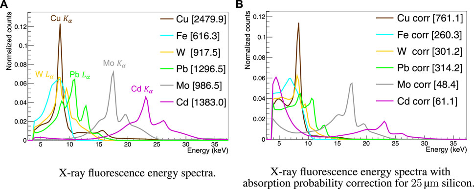
FIGURE 1. Energy spectra for the six X-ray fluorescence target materials Cd, Cu, Fe, Mo, Pb and W. They are measured with the HEXITEC detector, a pixel sensor optimized for X-ray detection through 1 mm thick CdTe as shown in (A). Spectra are corrected with the absorption probability in 25 µm silicon (B). All spectra are normalized and the normalization constants are stated in the legend in units of 105 counts.
2.2 The DECAL sensor
The digital summation logic in strip and pad mode was already shown to function in an earlier variant of the sensor with a thinner epitaxial layer of 18 µm silicon [3, 15]. This includes tests under laser illumination verifying the simulated charge collection. The second and current sensor variant aims for full depletion of the 25 µm epitaxial silicon layer through a gap in the n-layer, that goes along with an improvement in radiation hardness [4]. The DECAL pixel readout has been extensively described in [6]. The analog front end contains a charge-sensitive amplifier, followed by a shaping CR-RC unit. The shaper output is AC coupled to the comparator, which registers a hit when the shaper output voltage drops below a predefined threshold. A tuning logic is implemented through a dedicated 6 bit digital-to-analogue converter (DAC). It is applied by disconnecting shaper output and comparator input from a capacitor and instead charging it to a specific voltage using the tuning DAC. While one bit of the DAC is used for pixel masking, the other five bits define the voltage shift per pixel. A linear voltage response allows each shaper output to be fine-tuned relative to a global comparator threshold voltage. Once that voltage differential is applied, the tuning DAC gets disconnected and the AC coupling is reconnected to the shaper output and discriminator input. After tuning, the voltage baselines are aligned within a standard deviation of 1 mV when unmasking individual rows of the sensor [16]. However, the width and position of the voltage baseline is found to depend on the number of unmasked pixels. A threshold scan measures pixel counts in dependence of various threshold voltages. In the absence of a signal source, counts are detected only at threshold voltages close to the baseline and a so-called noise peak forms. Figure 2A shows such a scan of one strip for three different scenarios, where just this one strip is unmasked, where 10 and all 64 strips are unmasked. No signal source is present, so counts reflect the fluctuations of the shaper output due to thermal excitations in the sensitive silicon layer together with noise from the readout circuit. When many pixels are unmasked and tuned to the same voltage a threshold scan shows a wider noise peak. As shown in Figure 2B, the standard deviation describing the width of the noise peak increases from 3.1 mV to 6.4 mV (155 e− to 320 e−) when increasing the number of unmasked strips. The broadening of the noise peak originates from the pixel front end when a high digital activity of the firing comparators induces fluctuations. Due to this higher noise contribution, other comparators fire more often in the proximity of the noise peak. The broadening of the noise peak in terms of increasing standard deviation goes along with an increase of the shaper output. This is a global effect affecting all strips similarly as shown by the collective behaviour of a single strip and the sum of all unmasked strips as shown in Figure 2. While the wider noise peak degrades the separation of small signals from the noise peak, the application of DECAL in a sampling calorimeter targets a pixel threshold setting of at least 3 standard deviations away from the baseline. The requirement is a high detection efficiency for minimum ionizing particles (MIPs) that are created in an electromagnetic shower. Even for high particle fluences, the digital occupancy is much lower than in the case of setting the threshold to the noise level. The functionality of pixel masking has been implemented to detect single pixel noise for tuning purposes without the effect of excessive activity in neighboring pixels.
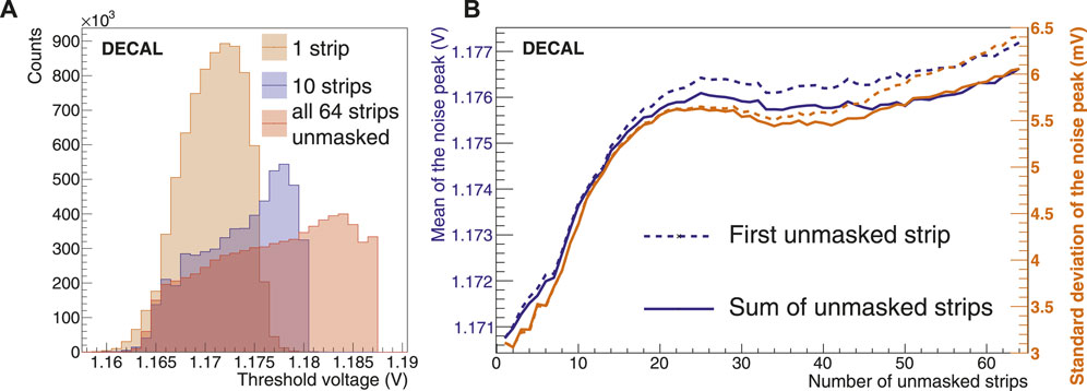
FIGURE 2. Noise peak broadening under high digital activity. Three scenarios of threshold scans of a single strip in the same time interval are presented in (A). While unmasking additional strips, the width and mean of the noise peak increase, as seen when comparing the noise peak when only one strip is unmasked with cases where in total 10 or all 64 strips are unmasked. The same behaviour is detected for the first unmasked strip as well as the sum of all unmasked strips (B).
Another undesired effect is found to be a drifting comparator input of the pixels with time. While the global threshold voltage is kept constant, the shaper output is AC coupled to the comparator input. The drift on this input amounts to 18.9 mV/ms on average with a standard deviation of the sample of 8.0 mV/ms. The clear source of the drift is still unknown. For all pixels the drift occurs solely as a decrease in voltage. The amplifier and shaper outputs of one analog test pixel are mirrored out and these do not show any drift. Also, the tuning logic is not regarded to induce the drift because it can be configured to set a positive or negative voltage differential to the shaper output, while the drift occurs in negative direction only. The relatively large standard deviation of the drift is explained through a large spread between pixels, that drift between 5 and 74 mV/ms. To mitigate the effect a pixel can be reset by disconnecting and subsequently reconnecting the shaper output with the AC coupling to the comparator input. After this, the comparator input is tuned to a reproducible starting value and begins to drift. The reset is regularly performed after 25 µs to keep the average drift of the shaper output well below 1 mV. Only hits during the 25 µs time windows are detected. The measurement setup includes a Field Programmable Gate Array (FPGA) board for communication between PC and the DECAL sensor. Owing to latency time in PC to FPGA communication a reset is feasible every 160 µs. This introduces an overall dead time of 135 µs, meaning that the sensor is only sensitive at 16% of the time.
2.3 DECAL threshold scans and spectra
Under X-ray illumination the energy of an absorbed photon in the epitaxial silicon layer creates electron-hole pairs. The digital readout of the DECAL sensor counts hits when the shaper output of a pixel drops below a defined threshold voltage. The noise peak forms through fluctuations of the shaper output, that cause hits only in the proximity of the baseline. A signal is induced on the readout electrode as a consequence of electron drift inside the active silicon epitaxial layer. The signal is then processed by an amplifier and shaper and leads to a drop in the shaper output. The presence of the signal, e.g., through an absorbed photon, creates a shoulder in the threshold scan below the noise peak. For monochromatic X-ray radiation a steep rise followed by a flat plateau is expected and can be parameterized by an error function. The rise of this shoulder to the low voltage side corresponds to hits when the threshold voltage is set to the maximum amplitude of the signal. The length of the shoulder is defined as the distance between the mean of the error function and the mean of the noise peak. It corresponds to the energy of the absorbed photon. Examples of the noise peak with shoulder can be seen in Figures 3A, C where photons from tungsten fluorescence are absorbed. They are scans of only one unmasked row and of all rows unmasked, respectively. The blue lines mark background scans in the absence of the X-ray illumination and describe the noise peak. The noise peak is symmetric for the single row scan where only 64 pixels are unmasked and is wider and skewed when unmasking all pixels as already described in Section 2.2. The signal shoulder below the noise peak is parameterized by a sum of two error functions. A second error function is needed here to account for the high energy tail in the X-ray spectra of Cu, Pb and W and for a low energy tail in the spectra of Cd and Mo. These tails can be identified in Figure 1. The spectrum is then differentiated which results in a Gaussian distribution in place of the error function. Additionally, the x-axis is inverted and the origin is chosen to be at the mean of the noise peak. This inverted value is then defined as the inverted voltage. According to
the differentiation of an error function results in a Gaussian distribution with parameter μ as the mean and half the variance. The differentiated spectra from tungsten fluorescence are shown in Figures 3B, D. By shifting the mean of the noise peak to the origin, the mean of the Gaussian μS characterizes the amplitude of the signal and coincides with the length of the signal shoulder described above. The main Gaussian peaks are centered at similar signal heights of 40 mV and 41 mV for single row and whole sensor unmasked respectively, despite of a wider noise peak in the latter case. The ratio of the height parameters h1 is expected to be 64, as the sensitive area is increased correspondingly when unmasking the whole sensor. Here, the ratio yields 62.0 deviating 3.1% from expectation. Taking the height ratios of all main peaks from the six target materials into account, a mean ratio is obtained of 62.9 ± 2.3. This shows a correct functionality of pixel masking, reducing the active area as expected. Moreover, the broadening of the recorded signal, as seen for the noise peak at high digital activity, does not occur at lower threshold voltages in the signal shoulder regime because the count rate is many orders of magnitude lower.
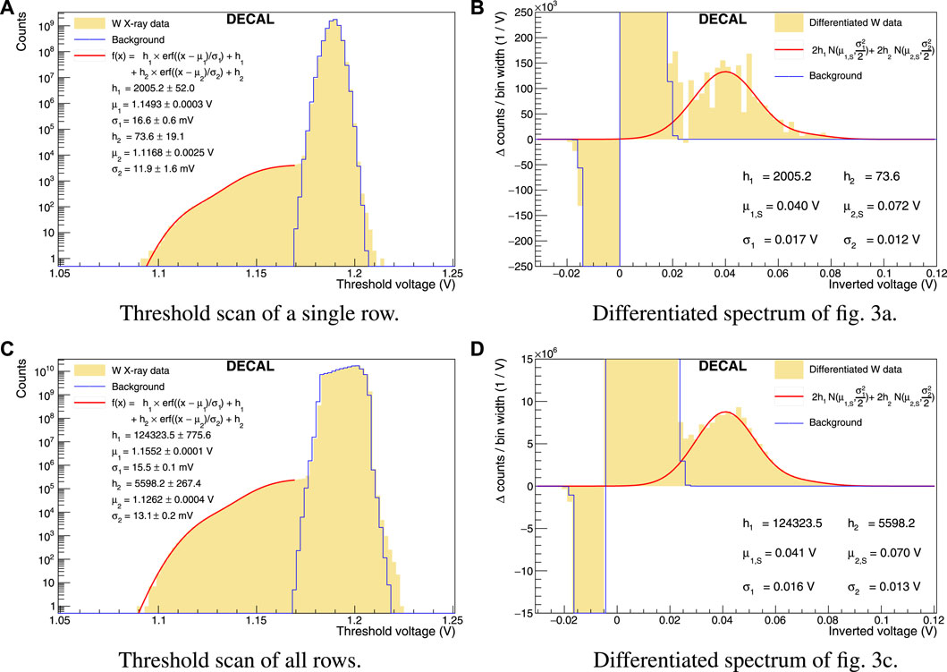
FIGURE 3. DECAL threshold scans and differentiated spectra under X-ray fluorescence of tungsten. (A) is a scan on logarithmic y-axis with a single row of 64 pixels not masked. The blue line is data recorded in the absence of fluorescence and hence models noise. The yellow histogram is the data including tungsten fluorescence and the red curve is a fit of error functions to the tungsten signal. (B) is the differentiated spectrum with an inverted and shifted x-axis. (C) and (D) show the corresponding data with all 64×64 pixels unmasked, resulting in a wider background noise peak (blue line) and more statistics of signal counts. The red curve in the threshold scans represents a fit of error functions to the tungsten signal whose analytical differentiation results in Gaussian distributions.
3 Results and discussion
In the DECAL pixel the created charge through photon absorption depends on the photon energy. This charge is collected in the small collection electrode and is then amplified and shaped. An energy calibration describes the signal at the shaper output in dependence of the photon energy. Through X-ray fluorescence of six target materials the energy range of 4–40 keV is covered and an americium-241 gamma-source extends that range up to the decay energy of 59.54 keV. For energy calibration two methods are presented. The first method involves comparing the peak position in the DECAL spectrum with the main excitation energy of the X-ray fluorescence. The second method relies on a reference detector optimized for X-ray detection and uses its energy spectra as fit functions to obtain an energy calibration as well as to estimate the energy resolution. Furthermore, the reference detector enables validation of the absolute count rate.
3.1 Energy calibration using the main excitation energies
The energy spectra from X-ray fluorescence of the six target materials exhibit peaks at the characteristic Kα and Lα energy levels as measured with the HEXITEC detector and presented in Figure 1. This allows to cross-check the excitation of the intended energy levels with an uncertainty of 1 keV, which is the specified full width at half maximum of the HEXITEC detector for the photon absorption at 59.5 keV [13]. Theoretical excitation energies from [14] are then used as reference for the peak positions in the DECAL spectra. As a parametrization, Gaussians are suitable to describe the spectra obtained with DECAL. The fit to the DECAL spectrum under tungsten fluorescence in Figure 3 results in μS = 41 mV as the mean of the Gaussian function. The main excitation Lα line of tungsten lies at 8.40 keV. Figure 4 combines the signal height parameters μS with the nominal excitation energies of all six target materials. The DECAL spectra for the other five target materials are presented in the Supplementary Material. An equivalent data point from an americium-241 gamma source is added at its decay energy of 59.54 keV. A linear model is suitable to describe the signal formation under photon absorption and finds the signal height per unit energy as the gradient
A linear response is found showing the functionality of the DECAL charge collection, signal amplification and shaping over the X-ray energy regime. Also, the y-intercept of the linear fit is located around the origin which proves that signal amplitudes are measured relative to the correct voltage baseline.
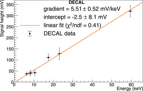
FIGURE 4. DECAL energy calibration by peak positions. The mean value μS from the differentiated spectra is plotted over the nominal X-ray peak energy for each target material. The uncertainty on the signal height is the width of the Gaussian peaks and the energy uncertainty is assumed to be 1 keV, the full width at half maximum of the HEXITEC peaks.
3.2 Energy calibration using the full X-ray absorption spectra
The second energy calibration method uses the measurement of the full HEXITEC energy spectra to calibrate the DECAL sensor rather than just using the main peak positions as done in the previous section. This is practical when the X-ray energy spectra are not clearly peaked or show multiple peaks making a main peak identification with a corresponding energy difficult. Figure 5 shows two examples of differentiated DECAL threshold scans for the whole chip being unmasked and exposed to copper and tungsten fluorescence. The spectra of the other targets are gathered in the Supplementary Material. The HEXITEC energy spectra are fitted with a normalization constant C as well as a multiplicative constant a for x-axis translation. This way a signal voltage V is obtained from a photon of energy E as
The first method (Section 3.1) does not rely on this assumption and has shown a linear dependence. For each X-ray target three different fits are performed with the above parameters. The first fit, indicated by the blue dashed line in Figure 5, takes the HEXITEC energy spectrum for each material as the shape for the fit function. These are the spectra already shown in Figure 1A. The black dashed line represents a corrected spectrum, correcting for the absorption probability in 25 µm silicon (Figure 1B), thus taking into account the suppression at higher energies because of the falling absorption probability with photon energies. In the final fit model (red curve in Figure 5), the reference spectrum is additionally smeared by convolution with a Gaussian function. The goodness of the fit models is quantified by χ2/ndf that approaches unity while improving the model. The final model is characterized by a value of 1.3. In summary, the measured DECAL spectrum is modelled as the true source emission spectrum, convolved with a DECAL efficiency function and a DECAL resolution function. The efficiency is taken into account by weighing the HEXITEC reference spectrum (considered having a flat efficiency) with the absorption probabilities of 25 µm silicon. The DECAL energy resolution is estimated by the fit parameter σE. It incorporates the width of the Gaussian smearing added in quadrature to the nominal HEXITEC peak width of σ = 0.43 keV, which follows from a FWHM of 1 keV. Table 1 collects the fit parameters for all six target materials sorted by their characteristic peak energies Epeak. Altogether, an average signal height per keV of absorbed photon energy is found as
It is in good agreement with the gradient m = 5.51 ± 0.52 mV/keV obtained in Section 3.1 through the energy calibration by peak positions. This agreement is important to substantiate the claim of a linear dependence of signal height and photon energy up to an energy of 60 keV as the americium measurement enters the determination of m but not of a. A 30% reduction on the uncertainty of a compared to m is achieved by including all spectral data. It is noted, that the nominal X-ray peak energies do not enter its calculation because HEXITEC is used for reference. This calibration procedure is especially useful when the X-ray spectra are not highly peaked at the characteristic energies but form multiple peaks or broad spectra. As a sensor characteristic, the conversion gain is proportional to a, when expressing each keV of photon energy as the number of electron-hole pairs produced. From the production energy of ϵ = 3.6 eV for each pair the average conversion gain of
is found. This is in good agreement with the conversion gain of 20 µV/e− already published in [6] and the gain obtained through electrons from the strontium-90 source that was found to be 19.97 µV/e−.
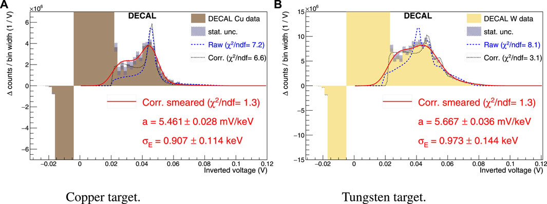
FIGURE 5. Spectrum of the inverted voltage obtained through scanning the threshold voltage under X-ray fluorescence with targets of (A) copper and (B) tungsten. For all X-ray target materials the raw HEXITEC energy spectra (dashed blue) and the ones corrected for the photon absorption probability in silicon (dashed black) are fitted. The spectra are scaled with a normalization constant C and multiplied in the voltage range by a factor a to translate from energy to voltage, according to Eq. 3. The corrected red curve incorporates a smearing by convolution with a Gaussian function whose standard deviation is expressed through an additional fit parameter σE. The statistical uncertainties (dashed area) are propagated from the bin entries of the threshold scans. Spectra of all six target materials as well as a table of all fit parameters are presented in the Supplementary Material.
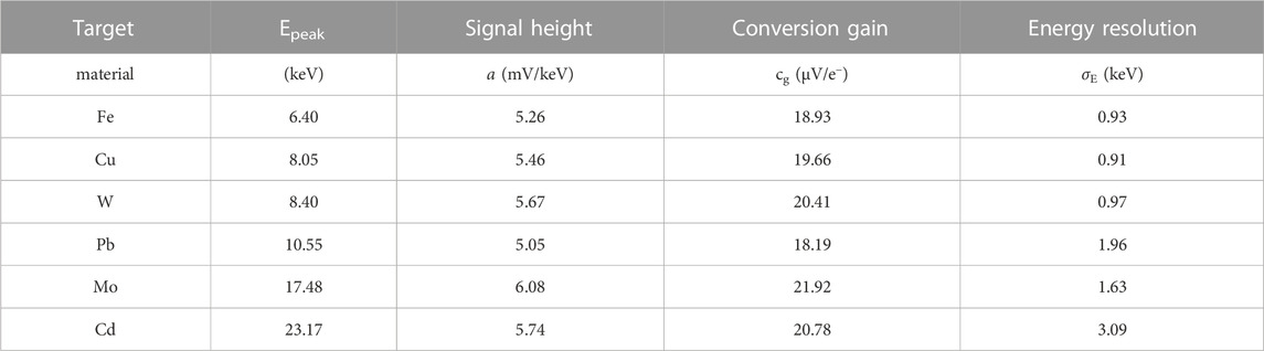
TABLE 1. DECAL signal height, energy resolution and conversion gain obtained from fitting the HEXITEC spectral shape to DECAL energy spectra. The DECAL sensor is exposed to X-ray fluorescence from six different target materials that emit photons close to their characteristic peak energies Epeak. The conversion gain is obtained by assuming one electron-hole pair produced for every 3.6 eV of photon energy.
The X-ray characterization enables estimation of a signal from a minimum ionizing particle (MIP). The mean energy loss of a MIP in silicon is 388 eV μm−1 [17]. Due to large tails in the energy loss distribution, a better experimental observable for single particle interactions is the most probable energy loss. For a MIP in 25 µm silicon the most probable loss is estimated to be 237 eV μm−1 [1, 17, 18]. Hence, the passing of a MIP through the DECAL epitaxial layer at shortest distance induces a signal equivalent to the photon absorption of a 5.9 keV photon. According to the energy calibration in Eq. 4, this corresponds to a signal of height 32.8 mV. This threshold lies 10.6 σ away from the baseline when considering the single strip noise and 5.1 σ for the noise after broadening.
3.2.1 Energy resolution
The energy resolution σE is estimated through Gaussian smearing of the reference spectra. As an example in Figure 5A, the DECAL peak width is greater than the dashed reference spectra. The fit parameter σE accounts for that and is plotted as a function of the X-ray fluorescence peak energies in Figure 6. An increase with energy is observed, that is compatible with a linear model. Under the assumption of a linear dependency, a relative energy resolution of
is obtained and presented for the first time for the DECAL sensor.
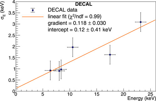
FIGURE 6. DECAL energy resolution as a function of the photon energy. The parameters σE describing the energy resolution in the spectral fits are plotted over the characteristic X-ray fluorescence energy. HEXITEC’s full width at half maximum being 1 keV is assumed to be the uncertainty on the fluorescence energy and the corresponding standard deviation the uncertainty on the energy resolution of each data point.
3.2.2 Expected and measured DECAL counts
Besides the energy calibration, discussed in the previous section, another important test is the comparison between the measured hits of the DECAL sensor and the expectation through the reference of the HEXITEC detector. The HEXITEC detector is used for reference because it absorbs all photons in the energy range of 4–40 keV due to its 1 mm thick CdTe pixels. During a measurement time of tH = 600 s the energy spectra in Figure 1A are recorded. The normalization constant quoted in Figure 1 of each spectrum gives the overall particle count. For estimating the DECAL counts it is crucial to account for the relatively thin silicon epitaxial layer of 25 µm. Not all photons passing through a DECAL pixel are absorbed and a correction of the reference energy spectra is necessary to estimate the DECAL counts. These corrected spectra from Figure 1B estimate the absorbed photons in the silicon epitaxial layer. The normalization constants CH of these spectra can be compared to the signal shoulder height of the DECAL threshold scans Cm. The signal shoulder height is estimated to be the number of counts measured within the duration of tD when the threshold voltage is set 19.6 mV below the mean of the noise peak. According to the first DECAL energy calibration in Section 3.1 the photon energy of 4 keV corresponds to a signal height of 19.6 mV. Thus the 19.6 mV offset accounts for the 4 keV cut-off after which HEXITEC is sensitive. For DECAL the amplitude corresponds to 6 standard deviations of the single strip noise and 3 standard deviations of the noise at high occupancy (Figure 2). To make the comparison between the sensors, additional information needs to be considered. First, the measurement times of HEXITEC, tH, and DECAL, tD, are different. Also, the sensitive area of HEXITEC, AH =400 mm2, and of DECAL, AD =12.39 mm2 are taken into account. Further, the X-ray tube current is raised between HEXITEC and DECAL measurements from IH to ID to provide sufficient counts for the DECAL measurement and avoid the saturation of HEXITEC which operates at a lower readout frequency of 1.591 kHz. The photon emission rate is expected to be proportional to the X-ray tube current, thus the amplification factor aI = ID/IH is introduced. All parameters that enter the calculation of the expected DECAL counts are summarized in Table 2. The expected DECAL counts are calculated as
In the second line of Eq. 7, constant parameters are already substituted. The expectation in scan type “Row” is further scaled down by a factor of 1/64, because only one of the 64 rows of the sensor is unmasked. The expected value Ce should be compared to the measured Cm.
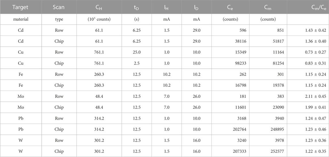
TABLE 2. Comparison of expected Ce and measured Cm DECAL counts. The expectation is calculated via Eq. 7 with the given parameters. The measured DECAL counts Cm are obtained from the error function to the threshold scan at a threshold voltage 19.6 mV below the mean of the noise peak. Finally, the ratio between measured and expected counts is given.
Having the measured DECAL counts Cm and the expected ones Ce at hand, their ratio is calculated and presented in Table 2. The uncertainty on the ratio is mainly determined by the uncertainty on the HEXITEC counts CH. The comparison of the different charge sharing modes in the HEXITEC software shows differences of up to 20% in the overall counts, motivating this as a relative uncertainty on CH. Another source of uncertainty is that the currents for the primary electron source IH and ID can be set with 0.1 mA precision. As a contribution from the DECAL threshold scan, the uncertainty on the measured counts in each threshold step is assumed to be the square root of counts, inherent for a Poisson counting process. All above sources of uncertainty contributions are propagated through the calculation of the ratio Cm to Ce. Other sources are negligible as the timing through the clock cycles of the electronics is assumed to be precise, such as the area of the sensors. Except for molybdenum - all measurements agree with expectations yielding a ratio compatible with unity. This agreement is far from trivial, recapitulating that DECAL and HEXITEC differ not only in pixel size and number, but are also based on different sensitive materials and make use of diverse readout frequencies. The 40 MHz readout frequency of DECAL corresponds to one frame taken every 25 ns. For an active measurement time tD of 12.5 s per threshold step 5 × 10⁸ frames are acquired. Other measurement times scale accordingly. For HEXITEC with its 1.591 kHz readout a frame is taken every 629 µs. During the time tH of 600 s for each target material 9.55 × 10⁵ frames are collected. On average 30% more counts are measured with DECAL than expected. One explanation is that the assumption of a linear dependence between photon fluence and X-ray tube current does not hold over the whole current regime. Variations in the photon fluence of order 12% have been seen between before and after a restart of the X-ray tube, contributing to an offset between HEXITEC and DECAL measurements, as the tube must be turned off before changing detectors. Charge sharing between neighboring pixels has been accounted for in the HEXITEC detector. The signals of neighboring pixels during one clock cycle are summed up and can thus account for charge sharing between pixels. In a similar way it is possible that charge sharing occurs between neighboring DECAL pixels, which has not been accounted for and can hence lead to over-counting, as one absorbed photon could induce a charge at multiple pixels. The depletion zone is limited to the epitaxial layer due to its higher resistivity compared to the silicon bulk [19]. Diffusion of generated charges in the bulk is not expected to contribute to the collected charge. The exact spatial profile of the depletion zone as well as the extent of charge sharing can be further investigated through edge transient-current technique. It is especially noteworthy, that the row and chip scans with the same target material are all compatible with each other and deviate on average by 5.4%. This speaks for the correct functionality of masking pixels in the row scan. The noise peak broadening when unmasking the whole chip as described in Section 2.2 does not effect the absolute number of counts for threshold voltages outside of the noise peak.
4 Conclusion
Depleted monolithic active pixel sensors provide the technology for a digital electromagnetic calorimeter, that relies on counting shower particles rather than detecting energy depositions. Specifically, the high granular DECAL sensor is a 64 × 64 pixel prototype for digital electromagnetic calorimetry and tracking with a readout at 40 MHz. Two undesired effects have been described. Noise increases as more pixels of the sensor are active under high occupancy for threshold voltages close to the baseline voltage of the sensor. Further, a drift of the output voltage of each pixel is observed, requiring regular resets of all pixels. Both effects must be addressed in future sensor designs. In this article the DECAL sensor has been characterized for X-ray absorption in the energy range of 4–60 keV. By scanning through the threshold voltage under X-ray illumination a spectrum is retrieved from the binary hit information. The energy calibration yields a signal height per unit energy of a = 5.54 ± 0.37 mV/keV. The findings suggest that the X-ray characterization enables estimation of a signal from a minimum ionizing particle. Its most probable energy loss when passing the DECAL epitaxial layer corresponds to the energy of 5.9 keV. The absorption of a photon of the same energy is detected through a signal of height 32.8 mV according to the energy calibration presented here.
Data availability statement
The raw data supporting the conclusion of this article will be made available by the authors, without undue reservation.
Author contributions
PA, LG, KN, FW, and SW contributed to the conceptualization of the project, JD and MW organized and provided the readout software and FPGA firmware. LF, IK, and HW performed and managed the measurements. LF carried out the formal analysis and original draft preparation. Research supervision by PA, JD, CI, IK, IS, HW, and SW. Project administration by PA, IS, and FW, funding acquired by PA, LG, CI, KN, GV, NW, FW, SW, and ZZ. All authors contributed to the article and approved the submitted version.
Funding
The project funding received from the UK Research and Innovation—STFC Grant No. ST/N002911/1, the Birmingham Particle Physics Consolidated Grants: ST/N000463/1, ST/N001125/1, ST/P005888/1 and the European Union’s Horizon 2020 Research and Innovation programme under Grant Agreement No. 654168. This publication was funded by Deutsche Forschungsgemeinschaft (DFG, German Research Foundation)—491245950.
Acknowledgments
The authors gratefully acknowledge the assistance of Sion Richards, Rhian Mair Wheater and Matt Wilson for granting access and providing support to the X-ray tube facilities of the Technology Department at STFC-RAL.
Conflict of interest
The authors declare that the research was conducted in the absence of any commercial or financial relationships that could be construed as a potential conflict of interest.
Publisher’s note
All claims expressed in this article are solely those of the authors and do not necessarily represent those of their affiliated organizations, or those of the publisher, the editors and the reviewers. Any product that may be evaluated in this article, or claim that may be made by its manufacturer, is not guaranteed or endorsed by the publisher.
Supplementary material
The Supplementary Material for this article can be found online at: https://www.frontiersin.org/articles/10.3389/fphy.2023.1231336/full#supplementary-material
References
1. Leroy C, Rancoita PG. Principles of radiation interaction in matter and detection. 4th ed. World Scientific) (2016). doi:10.1142/9167
2. Sirunyan AM, Tumasyan A, Adam W, Asilar E, Bergauer T, Brandstetter J, et al. Particle-flow reconstruction and global event description with the CMS detector. JINST (2017) 12:P10003. doi:10.1088/1748-0221/12/10/P10003
3. Benhammadi S, Dopke J, Guerrini N, Phillips P, Sedgwick I, Villani G, et al. DECAL: a reconfigurable monolithic active pixel sensor for use in calorimetry and tracking. PoS TWEPP2019 (2020):040. doi:10.22323/1.370.0040
4. Snoeys W, Aglieri Rinella G, Hillemanns H, Kugathasan T, Mager M, Musa L, et al. A process modification for CMOS monolithic active pixel sensors for enhanced depletion, timing performance and radiation tolerance. Nucl Instrum Meth A (2017) 871:90–6. doi:10.1016/j.nima.2017.07.046
5. Pernegger H, Bates R, Buttar C, Dalla M, van Hoorne J, Kugathasan T, et al. First tests of a novel radiation hard CMOS sensor process for Depleted Monolithic Active Pixel Sensors. JINST (2017) 12:P06008. doi:10.1088/1748-0221/12/06/P06008
6. Allport P, Benhammadi S, Bosley R, Dopke J, Fasselt L, Flynn S, et al. DECAL: a reconfigurable monolithic active pixel sensor for tracking and calorimetry in a 180 nm image sensor process. Sensors (2022) 22:6848. doi:10.3390/s22186848
7. Abada A, Abbrescia M, AbdusSalam SS, Abdyukhanov I, Fernandez JA, Abramov A, et al. FCC physics opportunities: future circular collider conceptual design report volume 1. Eur Phys J C (2019) 79:474. doi:10.1140/epjc/s10052-019-6904-3
8. ECFA Detector R&D Roadmap Process Group. The 2021 ECFA detector research and development roadmap. Tech Rep (2020). CERN. doi:10.17181/CERN.XDPL.W2EX
9. ALICE Collaboration. Letter of intent: a forward calorimeter (FoCal) in the alice experiment. Tech Rep (2020). CERN.
10. De Haas A, Nooren G, Peitzmann T, Reicher M, Rocco E, Röhrich D, et al. The FoCal prototype—an extremely fine-grained electromagnetic calorimeter using CMOS pixel sensors. JINST (2018) 13:P01014. doi:10.1088/1748-0221/13/01/P01014
11. Peitzmann T, Alme J, Barthel R, van Bochove A, Borshchov V, Bosley R, et al. Results from the EPICAL-2 ultra-high granularity electromagnetic calorimeter prototype. Nucl Instrum Meth A (2022) 1045:167539. doi:10.1016/j.nima.2022.167539
12. Alme J, Barnaföldi GG, Barthel R, Borshchov V, Bodova T, van den Brink A, et al. A high-granularity digital tracking calorimeter optimized for proton CT. Front Phys (2020) 8:568243. doi:10.3389/fphy.2020.568243
13. Seller P, Bell S, Cernik RJ, Christodoulou C, Egan CK, Gaskin JA, et al. Pixellated Cd(Zn)Te high-energy X-ray instrument. JINST (2011) 6:C12009. doi:10.1088/1748-0221/6/12/C12009
14. Berger M, Hubbell J, Seltzer S, Chang J, Coursey J, Sukumar R, et al. XCOM: photon cross section database: NIST standard reference database 8. Gaithersburg, MD: NIST (2013). doi:10.18434/T48G6X
15. Allport P, Bosley R, Dopke J, Flynn S, Gonella L, Kopsalis I, et al. First tests of a reconfigurable depleted maps sensor for digital electromagnetic calorimetry. Nucl Instrum Meth A (2020) 958:162654. doi:10.1016/j.nima.2019.162654
16. Kopsalis I, Allport P, Benhammadi S, Bosley R, Dopke J, Fasselt L, et al. Evaluation of the DECAL Fully Depleted monolithic sensor for outer tracking and digital calorimetry. Nucl Instrum Meth A (2022) 1038:166955. doi:10.1016/j.nima.2022.166955
17. Particle Data Group. Review of particle physics. Prog Theor Exp Phys (2022):083C01. doi:10.1093/ptep/ptac097
18. Bichsel H. Straggling in thin silicon detectors. Rev Mod Phys (1988) 60:663–99. doi:10.1103/RevModPhys.60.663
Keywords: complementary metal oxide semiconductor (CMOS), depleted monolithic active pixel sensor (DMAPS), tracking, digital calorimetry, ECAL, X-ray fluorescence, energy calibration, particle physics
Citation: Fasselt L, Allport PP, Benhammadi S, Bosley RR, Dopke J, Flynn S, Gonella L, Guerrini N, Issever C, Nikolopoulos K, Kopsalis I, Philips P, Price T, Sedgwick I, Villani G, Warren M, Watson N, Weber H, Winter A, Wilson F, Worm S and Zhang Z (2023) Energy calibration through X-ray absorption of the DECAL sensor, a monolithic active pixel sensor prototype for digital electromagnetic calorimetry and tracking. Front. Phys. 11:1231336. doi: 10.3389/fphy.2023.1231336
Received: 30 May 2023; Accepted: 06 October 2023;
Published: 17 October 2023.
Edited by:
Gianantonio Pezzullo, Yale University, United StatesReviewed by:
Daniele Paesani, Laboratori Nazionali del Sud (INFN), ItalyEleonora Diociaiuti, National Laboratory of Frascati (INFN), Italy
Julian Heymes, Paul Scherrer Institut (PSI), Switzerland
Copyright © 2023 Fasselt, Allport, Benhammadi, Bosley, Dopke, Flynn, Gonella, Guerrini, Issever, Nikolopoulos, Kopsalis, Philips, Price, Sedgwick, Villani, Warren, Watson, Weber, Winter, Wilson, Worm and Zhang. This is an open-access article distributed under the terms of the Creative Commons Attribution License (CC BY). The use, distribution or reproduction in other forums is permitted, provided the original author(s) and the copyright owner(s) are credited and that the original publication in this journal is cited, in accordance with accepted academic practice. No use, distribution or reproduction is permitted which does not comply with these terms.
*Correspondence: Lucian Fasselt, bHVjaWFuLmZhc3NlbHRAZGVzeS5kZQ==